^2
Superconducting Nanowire Single Photon Detectors On-Fiber
Abstract
We present a novel design of a superconducting nanowire single photon detector (SNSPD) fabricated on a core of a single mode optical fiber. The proposed design allows high overlap between the fiber light mode and the detector, and consequently, our fabricated devices can remain small in dimension and maintain speed of operation, without scarifying the detection efficiency. The on-fiber fabrication method is detailed, together with experimental results. The proposed method can be exploited in the future for the fabrication of other fiber coupled devices.
pacs:
85.25.Oj, 74.78.-w, 07.57.KpSingle photon detectors are needed in various fields of science and technology Natarajan et al. (2012); Hadfield et al. (2006, 2005); Gilbert and Hamrick (2000); Gobby et al. (2004); Grein et al. (2011); Day et al. (2003); Baselmans et al. (2008); Alaverdian et al. (2002). The main figures of merit used to qualify a single photon detector are: the detection rate, the detection efficiency, the jitter, and the dark counts rate. Superconducting nanowire single photon detectors (SNSPD) Gol’tsman et al. (2001) are considered as a promising technology for an optical detection in the visible to near-infra-red band Natarajan et al. (2012). Achieving high coupling efficiency () between the light source and the detector remains an outstanding challenge.
Maximizing requires focusing the input light on a detector, which is typically defined as a square (or a circle) with few micrometers side (or diameter), and is operated inside a cryostat. Methods based on free space optics Gol’tsman et al. (2001) or mechanical cryogenic positioning of an optical fiber in front of the the sample Hu et al. (2009) require complicated and expensive instruments, and suffer from poor alignment stability. Alternatively, methods based on fixed alignment of an optical fiber to the sample Miki et al. (2007); Slysz et al. (2006) suffer from a fiber-center to detector-center misalignment (referred hereafter as the center-to-center-misalignment or ) of a few micrometers at least Miller et al. (2011). For these fixed alignment procedures, an increase in the detector dimensions is inevitable, in order to keep high. As the detector recovery time is linearly proportional to its area Kerman et al. (2006); Annunziata et al. (2010), it is important to keep the detector as small as possible. For example, for a typical device, made of wide thick niobium-nitride wires folded to an area of , the recovery time is Kerman et al. (2006); Annunziata et al. (2010)
In the present work, we propose an alternative system configuration, in which the detector is fabricated on a tip of an optical fiber. The on-fiber fabrication allows precise alignment of the detector to the fiber core, where the light intensity is maximal, while keeping the device small and fast. The proposed devices are simple to operate, small in size and do not require complicated optical or positioning equipment.
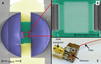
The complete fabrication process is done on the top facet of a zirconia ferrule, taken from a standard flat polished fiber connector (FC-UPC), holding a single mode fiber for the telecommunication bandwidth (Corning SMF-28 Cor ). The ferrule facet has a diameter of ; the fiber having a diameter is epoxy glued concentrically with the ferrule. We evaporate thick chromium film followed by a thick gold film trough a mechanical mask to form bonding pads. Next, a thick niobium nitride (NbN) film is deposited using a dc-magnetron sputtering system. The sputtering process is done from a niobium target in a vacuum chamber filled with mixture of argon and nitrogen gasses, while keeping the sample at room temperature Marsili et al. (2008); Bacon et al. (1983). The NbN film is covered in-situ with of aluminum.
To pattern the detector, we first narrow the NbN film to a wide bridge using a focused ion beam (FIB) system with a relatively high current (2.1\nA). During this step the aluminum layer protects the NbN film from an exposure to the ion beam, and reduces gallium poisoning Tettamanzi et al. (2009); Troeman et al. (2007); Yuvaraj et al. (2011). After the first lithography step, the aluminum layer is wet etched. The sample then undergoes a second lithography step, in which a meander is formed, using a low current () FIB patterning. A fabricated device can be seen in Fig. 1.
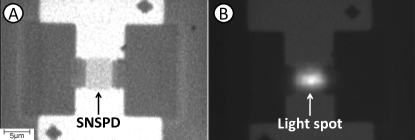
The FIB imaging system, which is used to align the detector to the fiber center, allows achieving of less than , limited mainly by the fiber-core to fiber-clad misalignment, given to be by Corning Cor . In Fig. 2 the low center-to-center-misalignment in our devices is demonstrated.
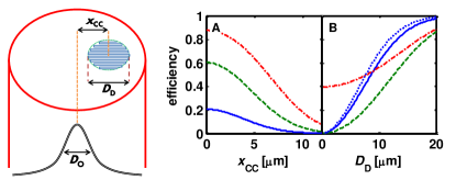
In order to estimate the effect of the center-center-misalignment on the detection efficiency, we calculate , namely the overlap between the Gaussian optical mode in an optical fiber Yariv (1985) and a detector located close to the top facet of the fiber:
| (1) |
where is the the mode field diameter and takes the a value of 1 if r is in the area of the detector, and vanishes otherwise. In Fig. 3 we plot for a several detectors, with several values, where we assume detector area fill-factor of and a SMF-28 fiber. We can see that for and relatively large detector with diameter of (panel A), is less then . Even for (panel B), is limited by for detectors with less then diameter. Note that for shorter wavelength fibers, the mode field diameter is even smaller and consequently misalignment results in even larger light loss.
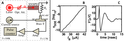
To characterize the detection performance, the fabricated device is inserted to a compact holder (Fig. 1C), and is wire bonded to a SMA connector. The SMA is used for both DC current bias and fast pulses output. The experimental setup is schematically presented in Fig. 4A. In Fig. 4B, we show the system detection efficiency (noted hereafter as ) as a function of the bias current in one of our devices. The critical current in the presented device is . The dark count, when the device is biased just below , is measured to be . Since does not saturate when approaching Natarajan et al. (2012) and since the dark count rate is low compared to other devices reported in literature Natarajan et al. (2012), we conclude that the level of the uniformity of critical current along the meander is relatively low in our device. Further work is needed to identify the underlying mechanisms that are responsible for the poor uniformity.
To summarize, we demonstrate a SNSPD fabricated on a tip of an optical fiber, with very low misalignment between the incoming light and the detector area. Though we achieve high coupling efficiency, more research is needed in order to increase the system detection efficiency. A future work in this direction may include adding an on-fiber optical cavity Baskin et al. (2012), changing the superconducting material to a one more suitable for deposition on the amorphous fiber Dorenbos et al. (2008); Marsili et al. (2012) and cooling the device to lower temperatures Engel et al. (2012).
This work was supported by the Mitchel Foundation, the Israel Ministry of Science, the Russell Berrie Nanotechnology Institute and MAFAT. The work of IB was supported by a Zeff Fellowship.
References
- Natarajan et al. (2012) C. M. Natarajan, M. G. Tanner, and R. H. Hadfield, Supercond, Sci. and Tech. 25, 063001 (2012).
- Hadfield et al. (2006) R. H. Hadfield, J. L. Habif, J. Schlafer, R. E. Schwall, and S. W. Nam, Appl. Phys. Lett. 89, 241129 (2006).
- Hadfield et al. (2005) R. H. Hadfield, M. J. Stevens, S. S. Gruber, A. J. Miller, R. E. Schwall, R. P. Mirin, and S. W. Nam, Opt. Express 13, 10846 (2005).
- Gilbert and Hamrick (2000) G. Gilbert and M. Hamrick, arXiv:quant-ph/0009027 (2000).
- Gobby et al. (2004) C. Gobby, Z. L. Yuan, and A. J. Shields, Appl. Phys. Lett. 84, 3762 (2004).
- Grein et al. (2011) M. Grein, A. Kerman, E. Dauler, O. Shatrovoy, R. Molnar, D. Rosenberg, J. Yoon, C. DeVoe, D. Murphy, B. Robinson, and D. Boroson, in Space Optical Systems and Applications (ICSOS), 2011 International Conference on (2011) pp. 78 –82.
- Day et al. (2003) P. K. Day, H. G. LeDuc, B. A. Mazin, A. Vayonakis, and J. Zmuidzinas, Nature 425, 817 (2003).
- Baselmans et al. (2008) J. Baselmans, S. Yates, R. Barends, Y. Lankwarden, J. Gao, H. Hoevers, and T. Klapwijk, J. Low Temp. Phys 151, 524 (2008).
- Alaverdian et al. (2002) L. Alaverdian, S. Alaverdian, O. Bilenko, I. Bogdanov, E. Filippova, D. Gavrilov, B. Gorbovitski, M. Gouzman, G. Gudkov, S. Domratchev, O. Kosobokova, N. Lifshitz, S. Luryi, V. Ruskovoloshin, A. Stepoukhovitch, M. Tcherevishnick, G. Tyshko, and V. Gorfinkel, Electrophoresis 23, 2804 (2002).
- Gol’tsman et al. (2001) G. N. Gol’tsman, O. Okunev, G. Chulkova, A. Lipatov, A. Semenov, K. Smirnov, B. Voronov, A. Dzardanov, C. Williams, and R. Sobolewski, Appl. Phys. Lett. 79, 705 (2001).
- Hu et al. (2009) X. Hu, T. Zhong, J. E. White, E. A. Dauler, F. Najafi, C. H. Herder, F. N. C. Wong, and K. K. Berggren, Opt. Lett. 34, 3607 (2009).
- Miki et al. (2007) S. Miki, M. Fujiwara, M. Sasaki, and Z. Wang, IEEE Trans. Appl. Superconduct. 17, 285 (2007).
- Slysz et al. (2006) W. Slysz, M. Wegrzecki, J. Bar, P. Grabiec, M. Górska, V. Zwiller, C. Latta, P. Bohi, I. Milostnaya, O. Minaeva, A. Antipov, O. Okunev, A. Korneev, K. Smirnov, B. Voronov, N. Kaurova, G. Gol’tsman, A. Pearlman, A. Cross, I. Komissarov, A. Verevkin, and R. Sobolewski, Appl. Phys. Lett. 88, 261113 (2006).
- Miller et al. (2011) A. J. Miller, A. E. Lita, B. Calkins, I. Vayshenker, S. M. Gruber, and S. W. Nam, Opt. Express 19, 9102 (2011).
- Kerman et al. (2006) A. J. Kerman, E. A. Dauler, W. E. Keicher, J. K. W. Yang, K. K. Berggren, G. Gol’tsman, and B. Voronov, Appl. Phys. Lett. 88, 111116 (2006).
- Annunziata et al. (2010) A. J. Annunziata, O. Quaranta, D. F. Santavicca, A. Casaburi, L. Frunzio, M. Ejrnaes, M. J. Rooks, R. Cristiano, S. Pagano, A. Frydman, and D. E. Prober, J. Appl. Phys. 108, 084507 (2010).
- (17) Corning Inc. wbsite http://www.corning.com.
- Marsili et al. (2008) F. Marsili, D. Bitauld, A. Fiore, A. Gaggero, F. Mattioli, R. Leoni, M. Benkahoul, and F. Lévy, Opt. Express 16, 3191 (2008).
- Bacon et al. (1983) D. D. Bacon, A. T. English, S. Nakahara, F. G. Peters, H. Schreiber, W. R. Sinclair, and R. B. van Dover, J. Appl. Phys. 54, 6509 (1983).
- Tettamanzi et al. (2009) G. C. Tettamanzi, C. I. Pakes, A. Potenza, S. Rubanov, C. H. Marrows, and S. Prawer, Nanotechnology 20, 5302 (2009).
- Troeman et al. (2007) A. Troeman, H. Derking, B. Borger, J. Pleikies, D. Veldhuis, and H. Hilgenkamp, Nano Lett. 7, 2152 (2007).
- Yuvaraj et al. (2011) D. Yuvaraj, G. Bachar, O. Suchoi, O. Shtempluck, and E. Buks, arXiv:1107.0635 (2011).
- Yariv (1985) A. Yariv, Optical electronics (Holt, Rinehart and Winston, 1985).
- Baskin et al. (2012) I. Baskin, G. Bachar, K. Shlomi, O. Shtempluck, and E. Buks, arXiv:1210.7327 (2012).
- Dorenbos et al. (2008) S. N. Dorenbos, E. M. Reiger, U. Perinetti, V. Zwiller, T. Zijlstra, and T. M. Klapwijk, Appl. Phys. Lett. 93, 131101 (2008).
- Marsili et al. (2012) F. Marsili, V. Verma, J. Stern, S. Harrington, A. Lita, T. Gerrits, I. Vayshenker, B. Baek, M. Shaw, R. Mirin, and S. Nam, arXiv:1209.5774 (2012).
- Engel et al. (2012) A. Engel, K. Inderbitzin, A. Schilling, R. Lusche, A. Semenov, H. Hübers, D. Henrich, M. Hofherr, M. Siegel, et al., arXiv:1210.5395 (2012).