Spin polarization and magnetoresistance through a ferromagnetic barrier in bilayer graphene
Abstract
We study spin dependent transport through a magnetic bilayer graphene nanojunction configured as two dimensional normal/ferromagnetic/normal structure where the gate-voltage is applied on the layers of ferromagnetic graphene. Based on the fourband Hamiltonian, conductance is calculated by using Landauer Butikker formula at zero temperature. For parallel configuration of the ferromagnetic layers of bilayer graphene, the energy band structure is metallic and spin polarization reaches to its maximum value close to the resonant states, while for antiparallel configuration, the nanojunction behaves as a semiconductor and there is no spin filtering. As a result, a huge magnetoresistance is achievable by altering the configurations of ferromagnetic graphene especially around the band gap.
pacs:
73.23.-b,73.63.-bI Introduction
Since spin-orbit coupling in graphene novoselov is very weak spinorbit and also there is no nuclear spinhyperfine , spin flip length is so long about in dirty samples and room temperaturespinlength . Clean samples are expected to have longer spin coherency. This is good opportunity for spintronic applications based on candidatory of graphene. On the other hand, graphene has not intrinsically ferromagnetic (FM) properties, however, it is possible to induce ferromagnetism externally by doping and defectsdefects , Coulomb interactions coulomb or by applying an external electric field in the transverse direction in nanoribbonselectric . Recently, HaugenHaugen proposed the FM correlations due to strong proximity of magnetic states close to graphene. The overlap between the wave functions of the localized magnetic states in the magnetic insulator and the itinerant electrons in graphene induces an exchange field on itinerant electrons in graphene giving rise spin splitting of the transport. The exchange splitting which is induced by FM insulator Euo in graphene was estimated to be of order of . This splitting which is effectively similar to a Zeeman interaction has so large magnitude that can have important effects. Such spin splitting can be directly evaluated from the transmission resonances or magnetoresistance of FM graphene junction. The ferromagnetism leads to a spin splitting effectively similar to a Zeeman interaction but of much larger magnitude. The induced exchange field is tunable by an in-plane external electric fieldex-tune . The possibility of controlling spin conductance in FM monolayer graphene insulator has also been studied by Yokoyama Yokoyama . It was found that the spin conductance has an oscillatory behavior in terms of chemical potential and the gate voltage.
Bilayer graphene on the other hand has shown to have interesting properties for application in nanoelectronic devices such as transistors based on graphene substrate. The new type of integer quantum Hall effects QHE and also the electronic band gap controllable by vertically applied electric field are of its unusual properties in compared to monolayer graphene4band ; gap-BG ; gap-BG1 ; gap-BG2 . Moreover, the parabolic band structure close to the Dirac points transforms to a Mexican-hat like dispersion when an electric field is applied on graphene. Optical measurements and theoretical predictions propose a meV gap in bilayer graphene. This controllable gap makes bilayer graphene as an appropriate candidate for spintronic devices. An effective two-band Hamiltonian can describe the low energy excitations of a graphene bilayer in the regime of low barrier heightseffective2band . However, the four-band Hamiltonian is known to give a better agreement with both experimental data and theoretical tight-binding calculationsbarbier ; 4band . Very recently, spin splitting of conductance in bilayer graphene has been investigated by using an effective two-band Hamiltonian emerging from low energy approximationYu . This approximation is valid when energy of electrons hitting on the potential barrier is about the barrier height. Application of a potential difference between upper and lower layers intensifies the failure of this approximation. On the other hand, magnetoresistance in bilayer graphene has been studied in Ref.semenov by using Hamiltonian when the induced exchange fields are laid in plane of each layer with a rotation in their orientations aginst each other. By using Kobo-Greenwood formula, they have investigated the dependence of conductivity and magnetoresistance on temperature and induced exchange field.
Motivated by these studies, based on the four-band Hamiltonian and close to the Dirac points, we study spin current through a magnetic barrier creating by use of the proximity of a ferromagnetic insulator on bilayer graphene. Conductance is calculated by use of Landauer-Buttiker formula at zero temperature. The parameters of the barrier, energy and angle of incident electrons can affect transport through a magnetic barrier classifying in the propagating or evanescent modes. The dependnce of resonant peaks in transmission on system parameters is proposed to follow a resonance condtion. We have found in some resonant energies and barrier parameters and also around the gapped region that a remarkable spin polarization and also magnetoresistance can be achieved.
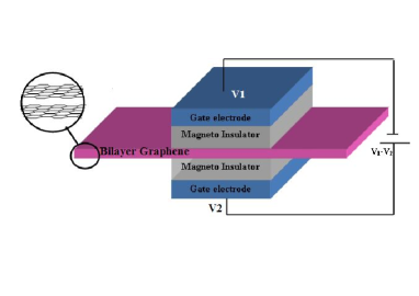
Model: We consider a normal/ferromagnetic/normal bilayer graphene nanojunction. The model we have used for a bilayer graphene sandwiched between two ferromagnetic insulator is shown schematically in Fig. 1. The exchange fields induced by the ferromagnetic insulators is supposed to be perpendicular to the graphene plane. Therefore, Hamiltonian of the spin up detaches from the spin down. Two gate electrodes can be attached to the ferromagnetic graphene from the upper and lower layers which control the barrier height in each of layers. This set-up is different from the systems studied by Refs.semenov ; nguyen . The exchange field splits this potential depending on the spin parallel or antiparallel () to the exchange field. So in the ferromagnetic part of bilayer graphene, we have where and are the exchange field and the potential barrier made by the gate voltage, respectively. So the two spins are scattered from the barriers with different heights. It means that energy shift of the top of the valance band in the barrier is different for parallel and antiparallel spins to the exchange field. This spin splitting causes to shift conductance as a function of energy for each spin resulting in magnetoresistance. To investigate spin polarization and also magnetoresistance, we have considered two different configurations so that the exchange field inducing by the magnetic insulators on each layer are parallel or antiparallel with respect to each other. The configuration prepared for observation of magnetoresistance differs from the configuration considered by Ref.semenov ; nguyen . The parallel configuration has a metallic behavior while the antiparallel configuration induces a potential difference between upper and lower layers concluding that the system has a semiconductor behavior with the band gap of .
This paper is organized as follows: we briefly explain the formalism which is used for calculating of transmission based on the four-band Hamiltonian. Before presenting our results, it is so important to have a short review in section III on transport through a barrier deposited on bilayer graphene and its dependence on the system parameters such as energy of incident quasi-particles and their angle hitting into the barrier and also barrier parameters. The method presented in section II is a detailed analysis accompanied with some small corrections on the method used by Ref.barbier . We will present spin polarization in the parallel configuration in section IV. Magnetoresistance and its dependence on energy of incident particles and also induced magnetic field will be investigated in section V. Finally, the last section concludes our results.
II Formalism
In the unit cell of bilayer graphene, we suppose that two independent sublattices A and B related to each monolayer graphene are connected to each other in the Bernal stacking. Close to the Dirac points and in the nearest neighbor tight binding approximation, the four band Hamiltonian and also its eigenfunction is written as the following:
| (1) |
where
and in the above formula where and are the incident angle and wave number of quasi-particles hitting on a barrier which is created by applying a bias to a metallic strip deposited on bilayer graphene. Moreover, and are the gate potentials applied on the upper and lower layers of bilayer graphene. Such a gate potential can be manipulated by applying a perpendicular electric field on graphene sheet. Here, the barrier is approximated by a square potential of barrier with sharp variation. By solving the eigenvalue equation of , the four band spectrum can be concluded as the following:
| (2) |
where the above parameters are defined as the following:
| (3) |
In the case of and , in low energy limit, energy spectrum behaves as where is an effective mass. This approximation which results in a effective two-band Hamiltonian is valid when energy of incident electrons is close to the barrier height. On the other word, in the case of zero potential difference between two layers, the absolute value of should be much smaller than the interlayer coupling strength (0.4eV). For , this approximation may fail for large potential differences. So one should care to choose valid energy and potential ranges. However, in spite of Ref.Yu , in this paper, we use four-band Hamiltonian in which the only approximation is the Dirac cone.
If we assume plane wave solution for the Schroedinger equation, the wave function in each region with a constant potential is written as the following matrix product.
| (4) |
where matrix elements of the matrices and are defined as the following:
| (5) |
| (6) |
Here is the wave number in the x direction and is defined as:
| (7) |
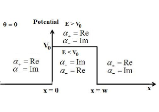
In the special case of normal incident angle and zero gate potential where , the wave number is real in the energy range of and is real if the energy of incident particles is in the range of . In this paper, studied system contains a magnetic or electrostatic barrier of potential as shown in Fig.2. The barrier width is . The electrostatic potential which plays the role of the gate voltage is set to be in the barrier part and zero in the first and last regions. We suppose that the energy range of incident particles is limited to the range of . Consequently in the barrier part we have . The wave numbers behind and in front of the barrier and are real while and are imaginary. In the barrier part, for , the wave numbers and are imaginary and real, respectively, while for they behave vice versa. A schematic view of the barrier at normal incidence and wave numbers in each part are shown in Fig.2.
By applying continuity of the wave functions on the boundaries of the barrier, one can connect coefficient matrix of the wave function for the last region to the coefficient matrix for the first region .
| (8) |
where N is called as transfer matrix. Since and are imaginary in the interested energy range, that part of wave function which are associated by such wave numbers are exponentially a growing or decaying function. So we have to set the coefficient of plane wave ( in Eq. 4) to be zero for the first region, because this part of wave function grows exponentially when . Therefore, coefficients matrix in the first region is supposed to be as , where the superscript refers to the transpose of a matrix and is the coefficient of growing evanescent state and is the coefficient of the reflected part of the wave function. In the last region, we have to set the coefficient ( in Eq. 4) of to be zero because this part of the wave function increases exponentially when . Therefore, the coefficients matrix in the last regions is supposed to be as where is the coefficient of the transmitted part of wave function and is the coefficient of decaying evanescent state. In this region, there is no reflected wave. However, in equation 8 of Ref.barbier , matrices and have been considered to be completely displaced which leas to different results.
By rearrangement of the transfer matrix elements of Eq. 8, the coefficient of transmitted part of wave function is derived in terms of transfer matrix elements as the following;
| (9) |
Since the first and last regions possess similar wave numbers, transmission probability is given as . Before presenting our results, in the next section, we will shortly review transport properties through a potential barrier by using the mentioned formalism.
III Transmission through a Barrier on Bilayer Graphene
The Klein tunneling in monolayer graphene results in a complete transmission through a barrier potential in normal incident. However, in contrast to monolayer graphene, as a result of chiral symmetry in bilayer graphene, transmission is zero for quasiparticles with energies lower than the barrier height. In the special case of , transmission through a potential barrier can be analytically calculated in normal incident and for two ranges of energy and .
| (10) |
where
where in the above formula, parameters are defined as . So the real part of the wave numbers inside and outside of the barrier part are defined as and , respectively. The energy of incident particle is supposed to be always . So is always real.
For the energy range of , the wave number inside the barrier part and consequently are imaginary so that and where and are real. As a result, transmission tends to zero as a function of the system parameters such as and .
| (11) |
This behavior is the trace of chiral symmetry in bilayer graphene. However, if the incident angle is nonzero, some resonant peaks appear in the transmission curve (see Fig. 4). For the energy range of , all parameters such as and are real. Thus transmission has an oscillatory behavior as a function of as the following form,
| (12) |
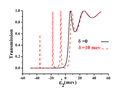
In the high energies limit , we have and so transmission is complete (). By applying a vertically electric field in the barrier part, a band gap is opened in the band structure of bilayer graphene which is proportional to the potential difference between potentials of each layers. In this case, chiral symmetry is failed and therefore transmission in normal incidence is nonzero for energies lower than the barrier height (). Transmission at normal incidence is represented in Fig. 3 as a function of for and . Application of a vertically electric field causes to emerge some resonant tunneling states for energies of . In this energy range, resonant states originates from interference of the incident and scattered waves. For all cases such as nonzero incident angles and , the resonant peaks are interpreted by the resonance condition relation proposed as
| (13) |
where is the x-component of the wave number inside the barrier which can be calculated by Eq. 7.
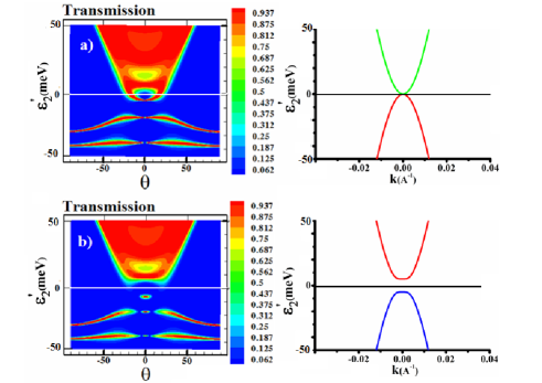
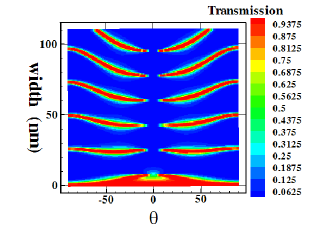
To have more complete view, we prepare a contour plot of transmission in plane of the incident angle and which is shown in Fig. 4 for a fixed width of the barrier. For the normal incidence (), transmission behavior is compatible with the results shown in Fig. 3.
For energies higher than the barrier height , transmitting channels are opened over all ranges of energies. However, transmitting window for the incident angles is limited with the condition that (in Eq. 7) is real. In the case of , the range of incident angle in which transmission is high can be extracted as . Therefore, by increasing , the range of angles with high transmission becomes more extended. In the energy range of , independent of the value of , resonant peaks emerge for nonzero incident angles () which obey the resonance condition . So additional to some resonant energy states, we have some resonant widths in which transmission is high. Fig. 5 shows transmission in plane of the incident angle and the barrier width for and . It is shown that based on the resonance condition (Eqs. 13,7), in large incident angles, reduces and so in a fixed resonance order (), the resonance condition is satisfied for wide barriers. Therefore, the resonance strips with complete transmission shown in Fig. 5, depend strongly on the incident angle in the range of wide barriers.
By applying a vertically electric field in the barrier part, a band gap is opened around . This band gap also has a trace in transmission as a transport gap shown in Fig. 4b.
IV Results
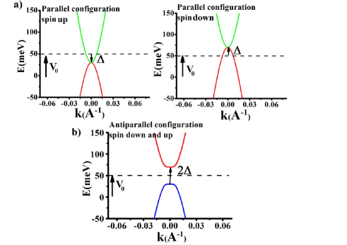
By application of an averaged gate voltage , band structure in the barrier part is shifted by value. Fig. 6 shows band structure of parallel and antiparallel configuration magnetic insulators when a gate voltage is applied on the barrier part. In case the exchange fields inducing in each layers of bilayer graphene are parallel, particles with spin parallel (spin up) and antiparallel (spin down) to the exchange fields are scattered from barriers with different heights. In the parallel configuration, spin splitting of the barrier potential in the ferromagnetic graphene is written as . Such spin splitting is also seen in the band structure that is shown in Fig. 6a. It is seen that the top of valance band are shifted to lower/higher energies for spins up/down. However, in the antiparallel configuration, the band structure shown in Fig. 6b is the same for both up and down spins. A band gap which is proportional to appears in the band structure of the antiparallel configuration.
IV.1 Spin Polarization
Here, there is a correspondence between the band structure and transmission. According to the band structure, we expect to emerge spin polarization just for parallel configuration because energy bands for up and down spins are shifted by with respect to each other. However, since the band structure for antiparallel configuration is the same for both spins, it is not expected to have spin polarization for this configuration. The spin polarization is defined as:
| (14) |
where and are conductance for up and down spins. The conductance is calculated by using Landauer formalism in the linear regime. Therefore, conductance is proportional to angularly averaged transmission projected along the current direction.
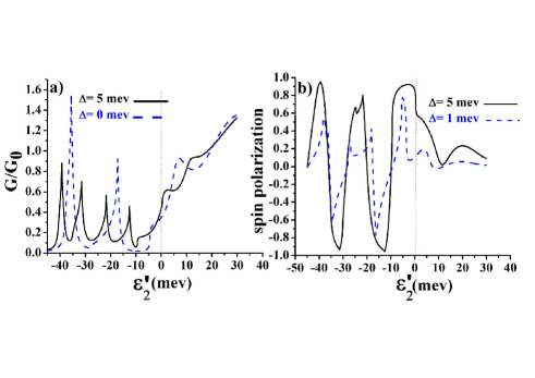
It is clear that additional to the transmission curves (Fig.4), resonance peaks also appears in conductance. Since up and down spins in the parallel configuration see barriers with different heights, resonance peaks in conductance as a function of Fermi energy are shifted to higher energies as for spin down and to lower energies as for spin up. This mismatching of conductance peaks for two spins causes to a large spin polarization at resonance states. Fig. 7 displays conductance and spin polarization as a function of for the parallel configuration. It is shown that conductance peaks and consequently spin polarization appears in the energy range of . It is seen that by inducing an exchange field, conductance peaks in Fig. 7a split into two peaks which are related to each spin. This spin splitting is about . Spin polarization shown in Fig. 7b has an oscillatory behavior with energy of incident particles for energies lower than the barrier height . The amplitude of spin polarization increases with the induced exchange field and reaches to its maximum value. However, spin polarization tends to zero for energies greater than the potential height except at .
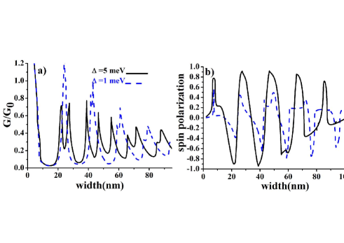
In the parallel configuration and for , Fig. 8a shows that conductance in the resonance widths has a peak. These peaks which are also seen in the transmission curves of Fig. 5 are explained by the resonance condition of Eq. 13. It is shown that spin splitting of conductance peaks also appears in the resonance widths which is originated from different barrier heights for two spins up and down. It should be noted that the conductance at resonance widths decreases for wide barriers. In the wide range of widths, the angularly window for transmitting channels shown in Fig. 5 decreases with the widths.
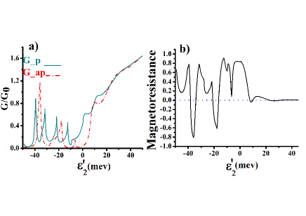
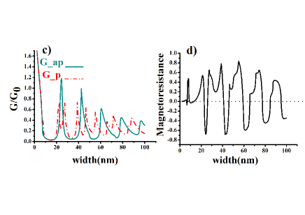
Fig. 8b shows spin polarization as a function of the barrier width. Again, spin polarization has an oscillatory behavior with the barrier width. The amplitude of spin polarization strongly increases by an increase of the induced exchange field. Therefore, to manifest this spin polarization, we should manufacture the ferromagnetic graphene part with the special widths in which spin polarization reaches to the value of unity.
IV.2 Magnetoresistance
In this section, we will show that by switching between parallel and antiparallel configurations, one can obtain large magnetoresistance. Magnetoresistance is defined as the following:
| (15) |
where and are conductance for parallel and antiparallel configurations.
Fig. 9 displays conductance in the parallel and antiparallel configurations and also magnetoresistance as a function of and the barrier width for a fixed exchange field . As we before expressed, spin splitting at the resonance states (for ) emerges in conductance peaks in the case of the parallel configuration. This behavior is clear in Fig. 9a and 9c. However, this splitting will not occur for the case of antiparallel configuration. Therefore, large magnetoresistance appears around the conductance resonance peaks. In the parallel configuration, a band gap appears around the barrier edge in the interval . This band gap has a trace in transmission and consequently conductance. Zero conductance region around the barrier edge which is seen in Fig.9a, is a result of the band gap. Since there is no such a band gap in the parallel configuration, magnetoresistance as shown in Fig.9b reaches to its maximum value in the energy band gap. In the energy range greater than the barrier height , there is no spin splitting and therefore, magnetoresistance tends to zero.
As we showed before, conductance has peak at resonant widths. Similar to the previous case, spin splitting occurs just for the parallel configuration. So magnetoresistance increases around the resonance widths. The oscillatory behavior of magnetoresistance as a function of the barrier width is represented in Fig.9d.
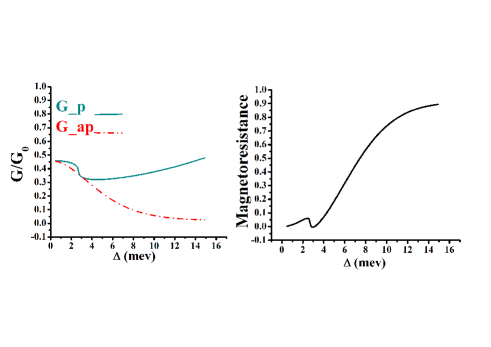
As we showed, there is a large magnetoresistance around the barrier edge . In this range of energies, we investigate the dependence of magnetoresistance to the induced exchange field. This exchange field of graphene can be controlled by an in-plane external electric field ex-tune . Fig. 10b represents that magnetoresistance increases monotonically by increasing the exchange field . It is interesting by increasing the exchange field up to , magnetoresistance reaches to its maximum value.
To explain this behavior, we investigate the dependence of conductance on the exchange field in the parallel and antiparallel configurations. In the antiparallel configuration, the band gap which is limited in the interval of , enhances by increasing the exchange field. Therefore, conductance in the antiparallel configuration goes to zero when the exchange field is increased. Suppression of the conductance with the exchange field in the antiparallel configuration is shown in Fig. 10a. However, in the parallel configuration, conductance increases by enhancement of the exchange field. The reason of this enhancement comes back to have larger angularly transmitting windows for larger (see Fig. 4). In fact, effective potential for spins up is decreased by an increase in . So for a fixed energy is increased and consequently and so is increased by . As a conclusion, for the exchange fields up to 10 meV, suppression of and an increase of results in a large magnetoresistance which is so useful for designing spin memory devices.
V Conclusion
We have studied spin polarization and magnetoresistance of a normal/ferromagnetic/normal junction of bilayer graphene by using transfer matrix method and based on the four-band Hamiltonian. Transport properties simultaneously is controlled by two gate electrodes (), which are applied on the ferromagnetic graphene. Two configurations of the exchange field is considered perpendicular to the graphene sheet. This exchange field is induced by the proximity of a localized magnetic orbital in a magnetic insulator coating on top of each layers of bilayer graphene in the barrier part. In the parallel configuration which graphene has a metallic behavior, a spin splitting occurs for the conductance at the resonant states just for energies lower than the barrier height . However, there is no spin splitting in the antiparallel configuration. A band gap of is opened in the antiparallel configuration which makes it a semiconductor. As a result of spin splitting in the parallel configuration, an oscillating spin polarization emerges for energies lower than the barrier height. Furthermore, an oscillatory of magnetoresistance with large amplitude is achievable for when we are able to switch between two configurations. There is also a large magnetoresistance in the energy range around the barrier edge originating from the band gap which is openned by a vertically electric field. In this range of energy, magnetoresistance reaches to its maximum value when the exchange field is increased by an in-plane external electric field.
References
- (1) K. S. Novoselov, A. K. Geim, S. V. Morozov, D. Jiang, Y. Zhang, S. V. Dubonos, I. V. Grigorieva, and A. A. Firsov, Science 306, 666 (2004).
- (2) D. Huertas-Hernando, F. Guinea, and A. Brataas, Phys. Rev. B. 74, 155426 (2006); Hongki Min, J. E. Hill, N. A. Sinitsyn, B. R. Sahu, L. Kleinman, and A. H. MacDonald, Phys. Rev. B. 74, 165310 (2006); Y. Yao, F. Ye, X. L. Qi, S. C. Zhang, and Z. Fang, Phys. Rev. B. 75, 041401, (2007).
- (3) B. Trauzettel, D. V. Bulaev, D. Loss, and G. Burkard, Nat. Phys. 3, 192 (2007).
- (4) N. Tombros, C. Jozsa, M. Popinciuc, H. T. Jonkman, B. J. van. Wees, Nature, 448, 571 (2007).
- (5) O. V. Yazyev and L. Helm, Phys. Rev. B. 75, 125408 (2007); T. O. Wehling, K. S. Novoselov, S. V. Morozov, E. E. Vdovin, M. I. Katsnelson, A. K. Geim and A. I. Lichtenstein, Nano Lett. 8, 173, (2008); N. M. R. Peres, F. Guinea and A. H. Castro Neto, Phys. Rev. B. 72, 174406 (2005).
- (6) N. M. R. Peres, F. Guinea, and A. H. Castro Neto, Phys. Rev. B. 72, 174406 (2005).
- (7) Y. W. Son, M. L. Cohen and S. G. Louie, Nature, 444, 347 (2006).
- (8) H. Haugen, D. Huertas-Hernando, A. Brataas, Phys. Rev. B. 77, 115406 (2008).
- (9) E.-J. Kan, Z. Li, J. Yang and J. G. Hou, Appl. Phys. Lett. 91, 243116 (2007)); S. Dutta and S. K. Pati, J. Phys. Chem. B. 112, 1333 (2008).
- (10) T. Yokoyama, Phys. Rev. B. 77, 073413 (2008).
- (11) K. S. Novoselov, et al., Nature Physics 2, 177 (2006).
- (12) T. Ohta, A. Bostwick, T. Seyller, K. Horn, and E. Rotenberg, Science 313, 951 (2006).
- (13) E. Castro, et. al., Phys. Rev. Lett. 99, 216802 (2007).
- (14) J. Oostinga, H. Heersche, X. Liu, A. Morpurgo, L. Vandersypen, Nat. Mater. 7, 151 (2008).
- (15) Y. Zhang, et. al, Nature, 459, 820 (2009).
- (16) E. McCann, V. I. Falko, Phys. Rev. Lett. 96, 086805 (2006).
- (17) M. Barbier, P. Vasilopoulos, F. M. Peeters and J. Milton Pereira, Phys. Rev. B. 79, 155402 (2009).
- (18) Y. Yu, Q. Liang, J. Dong, Phys. Lett. A. 375, 2858 (2011).
- (19) Y. G. Semenov, J. M. Zavada, K. W. Kim, Phys. Rev. B. 77, 235415 (2008); Phys. Rev. Lett. 101, 147206 (2008).
- (20) V. Hung Nguyen, A. Bournel, P. Dollfus, J. Appl. Phys. 109, 073717 (2011).