Opposite Changes in Gap Width of Opposite Spin States Induced by Rashba Effect in Anti-ferromagnetic Graphene on Ni(111)
Abstract
Graphene is a promising candidate for applications in spintronics. In this paper, Density Functional Theory method is used to calculate the band structure and magnetic properties of graphene on Ni(111). Our results show that once there is anti-ferromagnetic order in graphene, an external electric field at the order of V/m can induce a gap width difference of tens of meV for opposite spin states near the Fermi surface.
pacs:
PACS:I. INTRODUCTION
Graphene is a two-dimensional material with many interesting propertiesNovoselov and et.al. (2005, 2004); Zhang et al. (2005); Berger and de Heer et.al. (2006). Behavior of Dirac Fermions in graphene has been extensively studied. Particularly, magnetic properties have attracted lots of interests.
Graphene is considered a promising candidates for spintronics due to its long spin relaxation time and large spin relaxation lengthHill et al. (2006). Spin splitting is usually a desirable effect in potential applications. Although the intrinsic spin orbit coupling (SOC) is quite weakSemenov et al. (2007), considerable extrinsic SOC effects have been proposed and studiedKane and Mele (2005a, b); Yao et al. (2007); van Gelderen and Smith (2010); Min et al. (2006); Neto and Guinea (2009); Dedkov et al. (2008); Rader et al. (2009); Gierz et al. (2010); Semenov et al. (2007), among which the Rashba SOC resulted from broken inversion symmetry received lots of attention. The Rashba Hamiltonian can be expressed as
| (1) |
, , and respectively stands for Rashba strength parameter, electron momentum, Pauli spin operator and the electric filed.
Graphene/Ni system is studied here for two reasons: One is that graphene films can be conveniently prepared on Ni substrate; the other is that Ni is a common candidate for spin injection electrode and spin detection electrode. Published work suggests that the Rashba-induced spin gap can be as large as tens to hundreds of meVGong et al. (2011); Dedkov et al. (2008); Rader et al. (2009).
However, systematic study of the influences of Rashba effect on the Dirac fermions around the K point near the Fermi surface which greatly affect the transport properties is still lacking.
In this paper, we study few layer graphene(FLG)/Ni(111) system using density-functional theory (DFT) by considering various factors including substrate interaction, layer number and SOC.
II. METHODS
For First Principle Calculations LDA with PAW in VASPKresse and Furthmuller (1996a, b) has been used to optimize the Few Layer Graphene (FLG)/Ni system, which according to previous works is effective and sufficientHamada and Otani (2010). The energy cutoff of optimization is 500eV and the convergence criteria is that the Hellmann-Feynman forces be less than 0.03 eV/A for the geometry optimization. The graphene layers and upper three layers of the total six layers Ni(111) are allowed to relax. A vacuum slab more than is applied to avoid interaction between supercells.
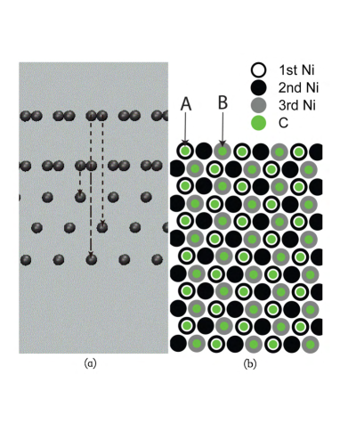
The original unit cell of Ni substrate is used, onto which the unit cell of graphene is mapped. In monolayer case the graphene is of the well studied top-fcc site, as shown in FIG. 1(b); for bilayer the bottom layer remains the same while the layer above is of hcp-fcc siteKarpan et al. (2007); Gamo et al. (1997); in case of more than two layers of graphene, an AB stacking model is used. This configuration is shown in FIG.1(a).
Then SOC is included into calculation to determine the influence of Rashba effect on the properties of monolayer case.
III. RESULTS AND DISCUSSIONS
The calculated band structures along for 1-4 layers of graphene on Ni(111) are demonstrated in FIG.2. We perform projected band structure calculation, in which the radius of red/blue spots demonstrates the weight of orbit of top layer graphene. FIG.2(a)/2(b) display band structure near Fermi surface for majority/minority spin of monolayer case, while that of bilayer, trilayer and quadrilayer are respectively shown in FIG.2(c)/2(d), 2(e)/2(f) and 2(g)/2(h).
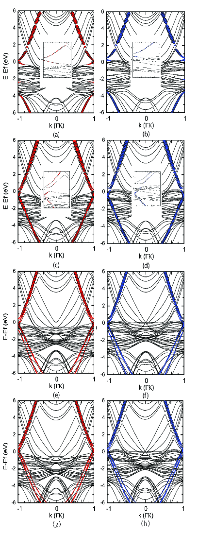
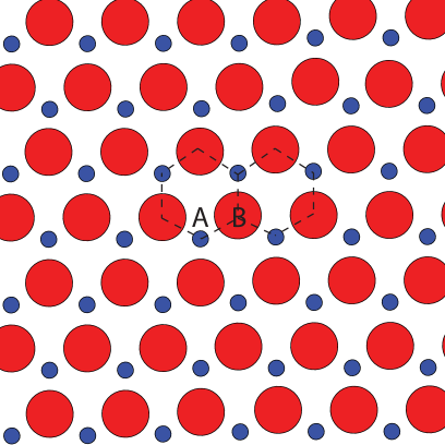
As is shown in FIG. 2(a) and 2(b), the existence of Ni substrate seriously changes the band structure of graphene compared with freestanding situation with gapless Dirac cone and linear energy dispersion. Due to the broken of the equivalence of the two sublattices of graphene caused by the substrate interaction, the Dirac Cone must be destroyed and a gap about 0.25eV opens up. The dense gray bands below the gap is those of Ni 3d orbit. The ferromagnetism of Ni leads to a 0.4eV spin gap, indicating the spin-polarized characteristics of graphene layer. The detail magnetization is displayed in FIG. 3, in which red and blue circle represents magnetism of C atoms parallel and anti-parallel to that of Ni atoms while the radius stands for the magnitude respectively. For convenience, the top layer Ni substrate is drawn as large gray circles. The graphene has an anti-ferromagnetic order, with one sublattice, namely A, under which is a first layer Ni atom, of magnetic momentum anti-parallel ( ) to that of Ni, and the other sublattice, namely B, of a parallel magnetism ( ).
For bilayer graphene, the parabolic energy dispersion is recovered since interation between graphene layers is weak. The Dirac point is lowered by about 0.4eV, suggesting strong charge transfer and vertical electric field, which can explain the small energy gap. And the spin gap is almost immeasurable, displaying the non spin-polarized character of top layer. Our calculation of the magnetization is also one magnitude lower than monolayer case. In Fig. 2(e) to 2(f), the energy of Dirac cone is at −0.2eV. In quadrilayer case, the Dirac Cone is almost at the Fermi Level, as shown in FIG. 2(g) and 2(h). This can be understood since less charge will be transferred to upper layer. And we expectedly find no difference between spins and negligible magnet moment.
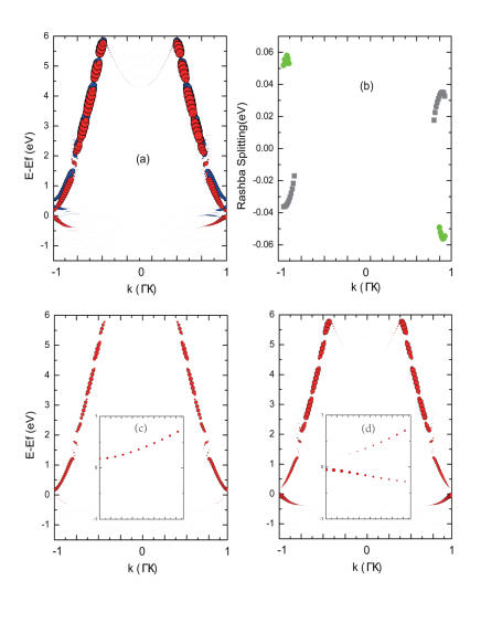
Thus from the discussion above, we conclude that the Ni substrate will result in a magnetization of graphene atoms and a vertical electric field. Both effects are weaken when layer number of graphene increase. Then Non-collinear Calculation is done for monolayer case since it has observable magnetization. We are interested in the band structure along near Fermi surface. The electric field E, as discussed above, is along the normal direction of Ni(111) surface, the measured wavevector is along , to which the magnetism of the system is set perpendicular in plane. The calculated band structure of monolayer case involving SOC is shown in FIG. 4(a), in which red/blue circles stand for bands of majority/minority spin with their radius representing weight of orbit of graphene atoms. The symmetry of bands is destroyed due to the linear dependence of Rashba splitting on wavevector. To determine the effect on spin gap of Rashba and exchange splitting individually, we do calculation of the same system both with/without SOC. With SOC, the spin gap will be , respectively representing the contribution of SOC and exchange splitting. If without SOC, only is included. In this way, we can show the individual Rashba splitting in FIG. 4(b). One important thing we should notice is that, for each spin in FIG. 4(a) there are two bands near the Fermi surface, one above the energy gap at K and the other below. Rashba splitting for upper/lower band is represented with grey squares/green circles in FIG. 4(b). It is critical that the Rashba splitting of upper (30meV) and lower (−60meV) bands are of different sign, which means that the energy gap of one spin at K will be enlarged while the other shrinked. This can be understood since the upper and lower bands near K and -K are mainly contributed by sublattice A and B respectively, see FIG.4(c) and 4(d). As has discussed above, the two sublattices are of opposite magnetism, which, according to Eq.(1), will result in opposite shift in spin gap. Due to the periodic boundary condition used in simulation, decreases to zero at the boundary of BZGong et al. (2011). Thus we evaluate it from near K and -K, which will be underestimated. The Rashba spin gap for upper band decrease sharply when getting away from K and -K(see the gray squares in FIG. 4(b)). This is because of the mixed contributions of both sublattices to the upper band at wavevector away from K and -K, as shown in FIG. 4(c) and 4(d). However, if we are focusing on band within 0.5eV around energy gap which mainly determains the transport property, the Rashba effect remains more than 30meV /-50meV. In cases of more than one layer of graphene, the Rashba effect on band structure of top layer also becomes inconsiderable due to the almost disappearance of magnetism.
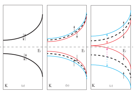
In this case, we have shown the comparatively large Rashba induced extra spin gap for bands at K near Fermi surface. In addition, the anti-ferromagnetic order and two sublattice character of graphene lead to the discrepancy of energy gap between spins. One will be enlarged for about 45meV and the other shrinked for about the same magnitude. Here the electric field in Rashba Hamiltonian is produced by the spontaneous charge transfer, which is approximately eV/Gong et al. (2010). Such effect can be tuned through extrinsic electric field perpendicular to the interface, and an electric field strong enough may completely close the gap for one spin and remarkably enlarge the gap for the other spin, which is the ideal situation in spintronics. FIG.5 is a schematic diagram in which we exclude exchange splitting and only consider Rashba effect. FIG.5(a) is the case with zero electric field and no Rashba effect, (b) is the Ni(111) case. It may be converted from semiconductor to half metal if we futher apply external electric field or strengthen the magnetization of graphene, as shown in FIG.5(c). Another critical implication is its application in valleytronics. Due to the linear dependence of Rashba splitting on wavevector, the degeneracy of the valley degree of freedom is broken and the shrink/enlarge effect is opposite at K/-K. This indicates that under proper configuration one spin may only transport at K and the other only at -K. Thus the Rashba effect we discuss here can also be an effective valley filter.
IV. CONCLUSINOS
In summary, graphene/Ni (111) are studied considering several factors including magnetism induced by substrate and Rashba effect. At last, the Rashba effect is found to produce a 30 meV/-60meV extra spin gap on upper/lower band at K near Fermi surface, which can further adjusts the spin gap with Rashba effect. In addition, the possibility to make discrepancy between energy gaps of different spin is discovered and interpreted, which provides a completely new method to efficiently optimize graphene/Ni system for the application in spintronics. And the opposite effect at K/K’ makes it also a promising valley filter. This method is tunable and can be extended to other systems with similar characters. Actually, we expect such effect in all graphene systems with different magnetization of two sublattices. Graphene on semiconductor substrate is desirable for application and SiC is a promising candidate. Another perhaps better system is carbon nanostructures without any substrate, which can display antiferromagnetic behavior due to topological frustrationWang et al. (2009). Graphene nanoribbon is an particularly expected choice, which is under way.
ACKNOWLEDGMENT
C.H.J. and Z.B. are supported by National Creative Fund for undergraduate. We thank Xiao Li and Junren Shi for helpful discussion.
References
- Novoselov and et.al. (2005) K. Novoselov and A. G. et.al., Nature 438 (2005).
- Novoselov and et.al. (2004) K. Novoselov and A. G. et.al., Science 306, 666 (2004).
- Zhang et al. (2005) Y. Zhang, Y.-W. Tan, H. L. Stormer, and P. Kim, Nature 438 (2005).
- Berger and de Heer et.al. (2006) C. Berger and W. A. de Heer et.al., Science 312, 1191 (2006).
- Hill et al. (2006) E. W. Hill, A. K. Geim, K. Novoselov, F. Schedin, and P. Blake, IEEE Trans. Magn. 42, 2694 (2006).
- Semenov et al. (2007) Y. G. Semenov, K. W. Kim, and J. M. Zavada, Appl. Phys. Lett. 91, 153105 (2007).
- Kane and Mele (2005a) C. L. Kane and E. J. Mele, Phys. Rev. Lett. 95, 226801 (2005a).
- Kane and Mele (2005b) C. L. Kane and E. J. Mele, Phys. Rev. Lett. 95, 146802 (2005b).
- Yao et al. (2007) Y. Yao, F. Ye, X. L. Qi, S. C. Zhang, and Z. Fang, Phys. Rev. B 75, 041401(R) (2007).
- van Gelderen and Smith (2010) R. van Gelderen and C. M. Smith, Phys. Rev. B 81, 125435 (2010).
- Min et al. (2006) H. Min, J. E. Hill, N. A. Sinitsyn, B. R. Sahu, L. Kleinman, and A. H.MacDonald, Phys. Rev. B 74, 165310 (2006).
- Neto and Guinea (2009) H. C. Neto and F. Guinea, Phys. Rev. Lett. 103, 026804 (2009).
- Dedkov et al. (2008) Y. Dedkov, M. Fonin, U. Rüdiger, and C. Laubschat, Phys. Rev. Lett. 100, 107602 (2008).
- Rader et al. (2009) O. Rader, A. Varykhalov, J. Sánchez-Barriga, D. Marchenko, A. Rybkin, and A. M. Shikin, Phys. Rev. Lett. 102, 057602 (2009).
- Gierz et al. (2010) I. Gierz, J. H. Dil, F. Meier, B. Slomski, J. Osterwalder, J. Henk, R. Winkler, C. R. Ast, and K. Kern, arXiv: 1004.1573 (2010).
- Gong et al. (2011) S. J. Gong, Z. Y. Li, Z. Q. Yang, C. Gong, C.-G. Duan, and J. H. Chu, J. Appl. Phys. 110, 043704 (2011).
- Kresse and Furthmuller (1996a) G. Kresse and J. Furthmuller, Comput. Mater. Sci. 6, 15 (1996a).
- Kresse and Furthmuller (1996b) G. Kresse and J. Furthmuller, Phys. Rev. B 54, 11169 (1996b).
- Hamada and Otani (2010) I. Hamada and M. Otani, PhysRevB. 82, 153412 (2010).
- Karpan et al. (2007) V. M. Karpan, G. Giovannetti, P. A. Khomyakov, M. Talanana, A. A. Starikov, M. Zwierzycki, J. van den Brink, G. Brocks, and P. J. Kelly, Phys. Rev. Lett. 99, 176602 (2007).
- Gamo et al. (1997) Y. Gamo, A. Nagashima, M. Wakabayashi, M. Terai, and C. Oshima, Surf. Sci. 374, 61 (1997).
- Gong et al. (2010) C. Gong, G. Lee, B. Shan, E. M, Vogel, R. M. Wallace, and K. Cho, J. Appl. Phys. 108, 123711 (2010).
- Wang et al. (2009) W. L. Wang, O. V. Yazyev, S. Meng, and E. Kaxiras, Phys. Rev. Lett. 102 (2009).