Andreev-reflection spectroscopy with superconducting indium - a case study
Abstract
We have investigated Andreev reflection at interfaces between superconducting indium (K) and several normal conducting non-magnetic metals (palladium, platinum, and silver) down to K as well as zinc (K) in its normal state at K. We analysed the point-contact spectra with the modified on-dimensional BTK theory valid for ballistic transport. It includes Dynes’ quasi-particle lifetime as fitting parameter in addition to superconducting energy gap and strength of the interface barrier. For contact areas from less than nm2 to nm2 the BTK -parameter was close to 0.5, corresponding to transmission coefficients of about , independent of the normal metal. The -parameter varies by less than around its average value, indicating that the interfaces have a negligible dielectric tunneling barrier. Also Fermi surface mismatch does not account for the observed . The extracted value can be explained by assuming that practically all of our point contacts are in the diffusive regime.
pacs:
85.30.Hi, 73.40.-c, 74.45.+cI Introduction
An interface between two conductors reduces charge (electron or hole) transport, transmitting a fraction of the incident current and reflecting the remainder . Normal reflection plays a central role in Andreev-reflection spectroscopy because also the Andreev-reflected holes can be normal reflected. The BTK theory for ballistic transport Blonder1982 assumes that normal reflection affects them both in the same way. This enables to measure the transmission coefficient of normal-superconductor interfaces. Ballistic transport requires that the electron mean free path is much larger than the contact diameter . Therefore one can reach the ballistic regime by making the contacts small enough. When the contacts are made larger, they become diffusive. In that case the elastic electron mean free path is much smaller than the contact diameter while the inelastic one is so large that the diffusive length still exceeds the contact diameter Lysykh1980 .
Blonder and Tinkham Blonder1983 explained the Andreev reflection double-minimum structure of ballistic contacts - an enhanced resistance around zero bias inside the energy gap - with a combination of tunnelling through a dielectric layer and the mismatch of Fermi velocities. By approximating the real dielectric barrier of width and height with a -function of strength and assuming free electrons with being the ratio of Fermi velocities and of the two electrodes, the transmission coefficient can be obtained from Blonder1983
| (1) |
Thus one could directly measure Fermi-velocity ratios once the contribution of the dielectric barrier is known.
In a typical Andreev-reflection experiment a dielectric oxide Simmons1964 or water/ice layer Repphun1995 has to be expected when the two electrodes and their contact are not prepared at ultra-high vacuum. And a junction between metals with different Fermi surfaces causes normal reflection since the electron wave functions have to be adjusted across the interface. Even a junction between two identical metals disrupts the crystal lattice and should lead to some amount of normal reflection. However, those effects are difficult to quantify.
Further complications arose when Steglich et al. Steglich1979 discovered heavy-fermion superconductors where the ’heavy’ conduction electrons with an extremely small Fermi velocity form the Cooper pairs. The first point-contact study of such compounds by U. Poppe Poppe1985 and Steglich et al. Steglich1985 focussed on Giaever-type tunneling to measure the density of states of the new superconductors and the Josephson effect to probe the symmetry of the heavy-fermion order parameter, without considering Andreev reflection. E. W. Fenton Fenton1985 predicted a huge normal reflection coefficient, corresponding to , for interfaces between a conventional and a heavy-fermion metal because of Fermi velocity mismatch. This idea got partial support by a large background residual resistance of heavy-fermion contacts where the cross-sectional area could be determined independently Gloos1995 ; Gloos1996a ; Gloos1996b . However, the expected tunneling-like Andreev reflection anomalies have not been found.
Deutscher and Nozières Deutscher1994 explained the weak normal reflection observed in Andreev-reflection experiments with heavy-fermion compounds by noting that the bare electrons and holes cross the interface, and not the heavy particles. This suggests that it is not the mismatch of Fermi velocities but that of the Fermi wave numbers that matters. Equation (1) remains valid with replaced by the ratio of Fermi wave numbers and of the electrodes. For interfaces between heavy-fermion compounds and conventional metals this ratio is of order unity, and therefore the parameter should be rather small. A number of point-contact Andreev reflection experiments on heavy-fermion compounds, for example Goll1993 ; DeWilde1994 ; Naidyuk1996 ; Park2008 , support this interpretation. Because heavy fermion metals often have an intrinsically short electron mean free path, it is possible that contacts with them are not ballistic but in the diffusive limit Gloos1996c ; Gloos1996b ; Gloos1998 .
Also the proximity effect at superconducting - normal metal thin film layered structures depends strongly on the transparency of the interfaces Attanasio2006 ; Kushnir2009 . These experiments reveal that (corresponding to ) for contacts between simple metals, considerably less than the expected () in free-electron approximation. The thin films are deposited in ultra-high vacuum, which excludes a dielectric interface barrier and leaves Fermi surface mismatch or a lattice discontinuity to explain the strong normal reflection.
One can also measure directly the current perpendicular to plane (CPP) resistance of an interface with a well-defined geometry and large cross-sectional areas of order m2 Pratt2009 ; Sharma2009 and compare it with electronic-structure calculations Xu2006 ; Xu2006b . The CPP resistance should contain information about normal reflection, but it is difficult to extract because of the lacking knowledge of the resistance without normal reflection.
Measuring electron spin polarization using Andreev-reflection spectroscopy Soulen1998 is another research topic that relies heavily on normal reflection and the ballistic nature of the contacts. According to the generally accepted view Bugoslavsky2005 ; Baltz2009 , the true spin polarization is obtained at highly transparent interfaces when while the measured polarization drops with increasing normal reflection. This strong dependence of the polarisation does not match the results of the Tedrow-Meservey tunneling experiments Tedrow1973 performed in the opposite limit, possibly indicating that the interface transparency affects the measured polarization in a complicated way Kant2002 ; Woods2004 .
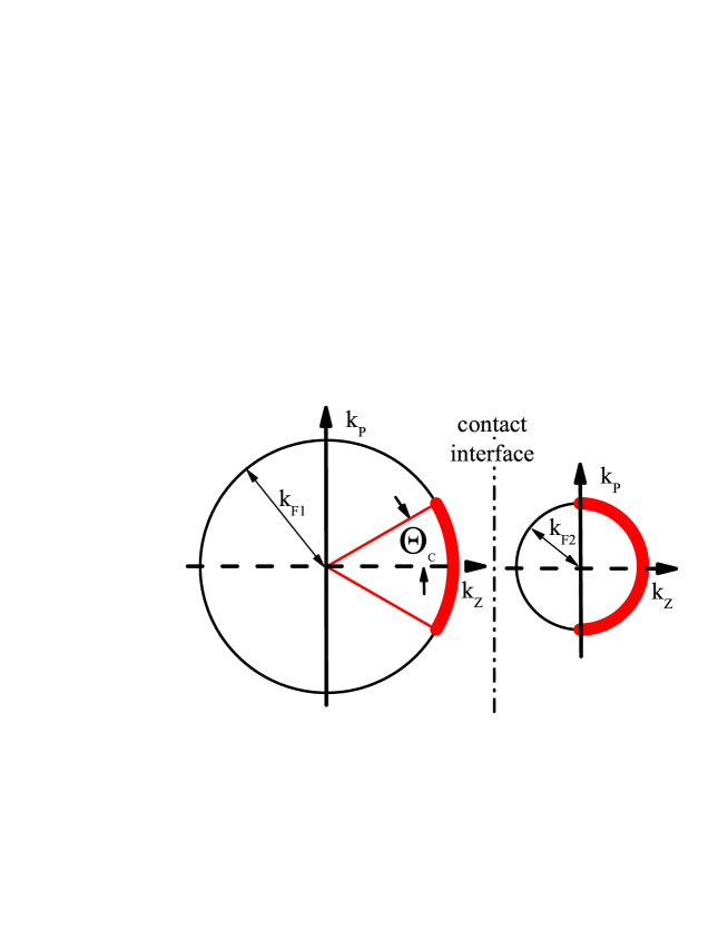
So far we have discussed normal and Andreev reflection in a one-dimensional model. Both become more complicated in three dimensions as shown schematically in Figure 1. Since the momentum component parallel to the contact plane is assumed to be conserved but not the perpendicular one, only particles with angle of incidence can be transmitted, all others are reflected Baranger1985 ; Kashiwaya1996 ; Mortensen1999 . Thus, when the superconductor has the larger one of the wave numbers, only part of its Fermi surface can be probed by Andreev-reflection spectroscopy. Total reflection does not occur in one dimension. A dielectric tunnelling barrier appears stronger in three than in one dimension because electrons or holes with off-axis incidence have a longer path through the barrier. Thus the one-dimensional BTK model over-estimates the -parameter Kashiwaya1996 ; Mortensen1999 . One hopes that the transition between one- and three-dimensional modelling would change the BTK parameters only slightly, and that the one-dimensional BTK model would remain valid and a good description of the experiments Kashiwaya1996 ; Mortensen1999 ; Daghero2010 .
In the one-dimensional BTK model is often treated as a simple fit parameter without further consideration. Using Andreev-reflection spectroscopy to determine material properties like the spin polarization or the symmetry of the superconducting order parameter requires understanding normal reflection because it is essential for electrical transport across an interface. We show here for contacts between superconducting indium (In) and several non-magnetic normal-conducting metals that in most cases the parameter is probably neither related to a dielectric barrier nor to Fermi surface mismatch. Assuming that the contacts down to atomic size are in the diffusive regime would naturally explain our results.
II Experiments and results
Point-contact experiments with superconducting indium (In) have a long history - junctions between In and normal metals have been investigated by Chien and Farrel Chien1975 even before the BTK theory became established. Our contacts were fabricated using the shear (crossed wire) method by gently touching one sample wire with the other one as described by J. I. Pankove Pankove1966 and more recently by Chubov et al. Chubov1982 . The In wires had mm diameter to provide extra mechanical rigidity as much thinner wires would bend too easily when the contacts are made. The silver (Ag), palladium (Pd), platinum (Pt), and zinc (Zn) wires had mm diameter. The contacts were measured below the critical temperature K of In down to 0.1 K in the vacuum region of a dilution refrigerator. A DC current with a small superposed AC component is injected into the contact and the voltage drop across the contact measured to obtain the characteristics as well as the differential resistance spectrum .
Point contacts with In were more difficult to fabricate than those with aluminium (Al) Gloos2012 . Very often, when we tried to set the resistance, the contact either opened with a vacuum gap between the electrodes or closed with an extremely small resistance of order m which is unsuitable for spectroscopy. We attribute this behaviour to the softness of In.
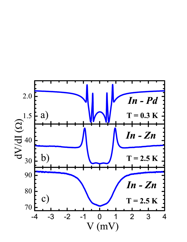
We classify the spectra as follows: 81% of the contacts had the typical Andreev reflection double-minimum anomaly and were further analysed. 5% of the contacts had additional anomalies, like a dip at zero bias, that we tend to attribute to proximity-induced superconductivity in the normal metal. The remaining 14% of the contacts showed spectra as in Figure 2 with excessive side peaks or with anomalies that we do not really understand and which we do not consider further. Table 1 lists the details for the investigated normal conductors.
| normal metal | total contacts | Andreev | proximity-like | undefined |
|---|---|---|---|---|
| Ag | 83 | 71 | 2 | 10 |
| Pd | 84 | 59 | 8 | 17 |
| Pt | 26 | 26 | 0 | 0 |
| Zn (at 2.5 K) | 44 | 37 | 2 | 5 |
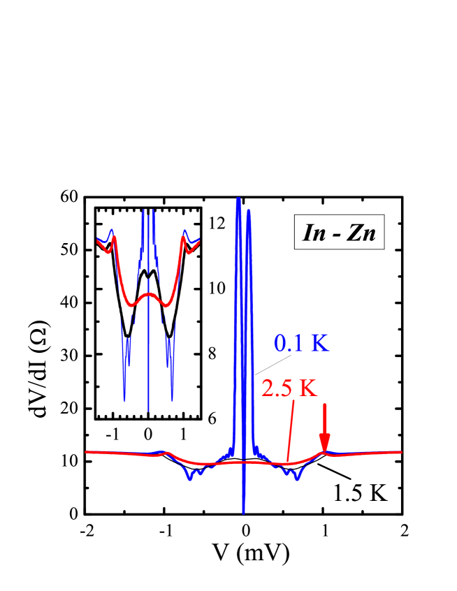
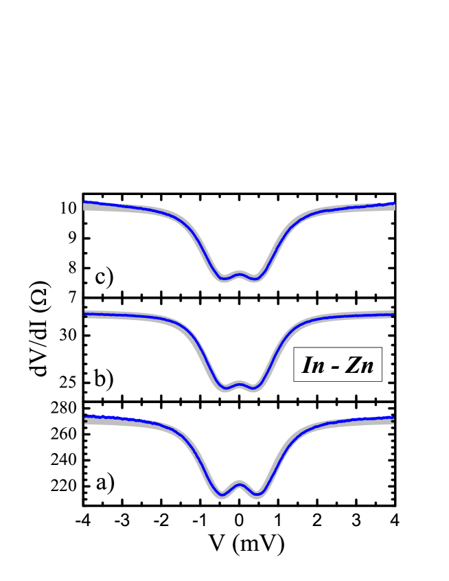
At low temperatures the contacts with Zn had typical Josephson-type characteristics with multiple Andreev reflection as presented in Figure 3. The temperature has to be raised to 2.5 K, well above the critical temperature K, of Zn to suppress the Josephson-type and proximity-like anomalies in most junctions. Although this procedure strongly reduces the magnitude of the Andreev-reflection signal, the -parameter can still be extracted.
The chosen spectra were analysed using a modified BTK theory that includes Dynes’ lifetime parameter Plecenik1994 , so that in total the model contains three adjustable parameters. The normal resistance was defined as the differential resistance at large bias voltages. Side peaks at finite bias voltage, for example due to the self-magnetic field Gloos2009b , were usually easy to recognize and did therefore not affect the analysis with respect to the -parameter.
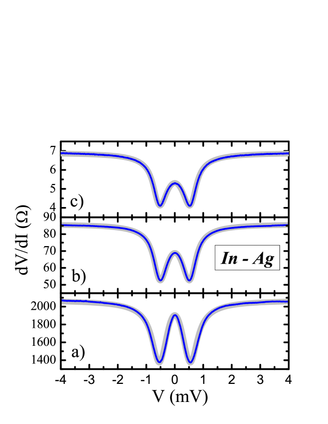
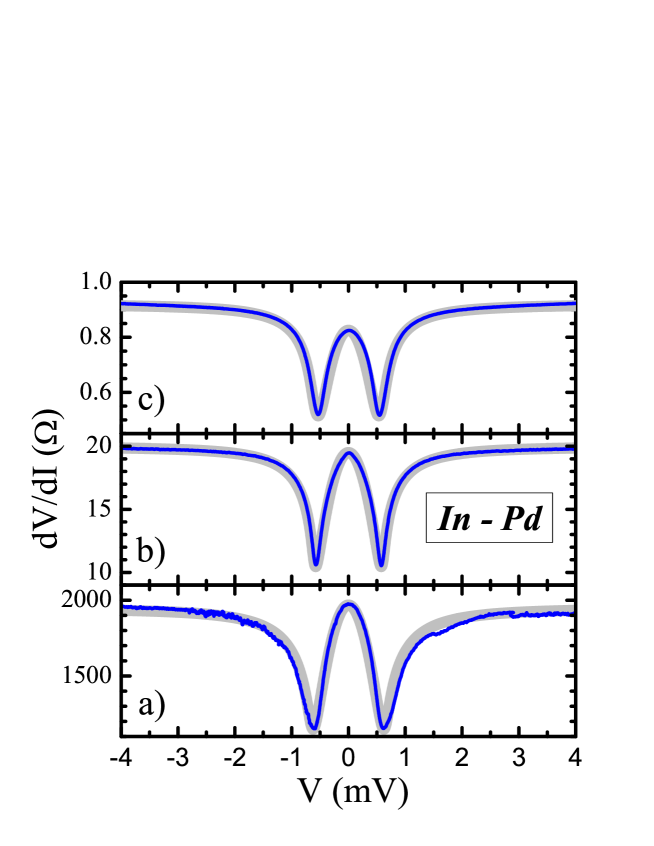
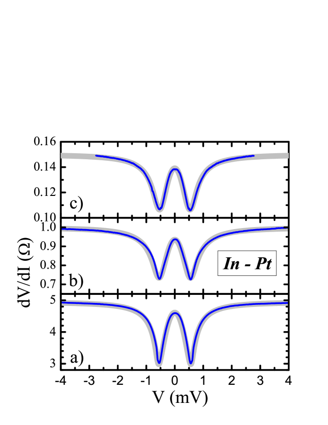
Figures 4, 5, 6, and 7 show selected spectra of superconducting In in contact with Ag, Pd, Pt, and Zn over the accessed resistance range together with a fit using the modified BTK model. Note that this is a one-dimensional model valid for ballistic transport. Table 2 summarizes the extracted fit parameters.
| metal | (meV) | (meV) | |||
|---|---|---|---|---|---|
| 6.9 | 0.7 | 1.18 | 0.025 | 0.420 | |
| Ag | 86.0 | 0.7 | 1.14 | 0.030 | 0.445 |
| 2071 | 0.7 | 1.17 | 0.063 | 0.535 | |
| 0.92 | 0.40 | 1.14 | 0.020 | 0.505 | |
| Pd | 20.0 | 0.13 | 1.20 | 0.025 | 0.550 |
| 1950 | 0.1 | 1.30 | 0.060 | 0.580 | |
| 0.15 | 0.5 | 1.14 | 0.110 | 0.540 | |
| Pt | 1.00 | 0.3 | 1.17 | 0.145 | 0.545 |
| 4.95 | 0.1 | 1.19 | 0.060 | 0.530 | |
| 10.16 | 2.5 | 1.30 | 0.045 | 0.485 | |
| Zn | 32.4 | 2.5 | 1.22 | 0.030 | 0.495 |
| 275 | 2.5 | 1.23 | 0.040 | 0.555 |
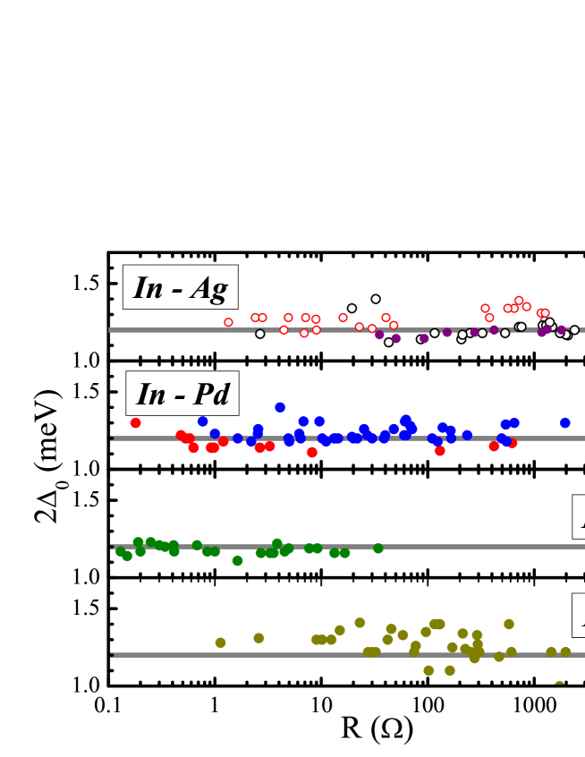
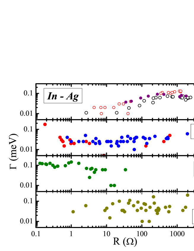
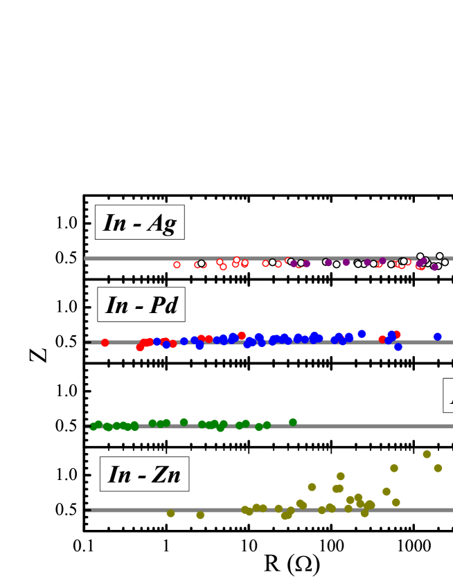
Figures 8, 9, and 10 show the derived parameters , , and as function of normal resistance for contacts between superconducting In and normal conducting Ag, Pd, Pt, and Zn, respectively. The energy gap meV is roughly constant from up to k. Most contacts have a that varies between eV and eV without a clear tendency. The lifetime parameter grows slightly with increasing resistance only for the contacts with Ag, independently of the temperature. The -parameter stays constant at 0.5 from up to several k and varies by less than from one normal conductor to another one. Larger -values appear for In - Ag junctions in the k range and for the In - Zn contacts above .
III Discussion
The BTK parameters of our contacts with superconducting In correspond well with those of superconducting Al Gloos2012 . Unlike of Al, that increases with , the In contacts have a rather constant meV. A systematic increase of with like for the Al contacts has only been found for In - Ag contacts, but to a lesser degree. For contacts with the other normal-conducting metals ranges from eV to eV. However, most notable is over up to five orders of magnitude in normal state resistance like for superconducting Al Gloos2012 . Point contacts with superconducting Nb, measured at K, have slightly larger average Z but with a wider variation Tuuli2011 . In the discussion we will focus on the seemingly universal value of .
Contact diameter. We estimate the contact diameter with the ballistic Sharvin resistance where . In free-electron approximation the used metals have Fermi wave numbers nm-1 Ashcroft1976 . Then a contact has a diameter of nm, assuming circular symmetry, or cross-sectional area. Thus our study covers contact areas from nm2 to less than nm2. According to the residual normal-state resistivity of the bulk metals we estimate elastic mean free paths of nm. Therefore contacts with normal resistance should be ballistic, justifying our use of the BTK model.
Superconducting energy gap. The energy gap meV is almost constant from around up to about k. The ratio is larger than the BCS value 3.52 and the tunnelling-derived bulk value of 3.58 Averill1972 . A slightly enhanced energy gap has been found earlier for In break junctions Gloos1999 . These deviations could be caused by the pressure or lattice distortion at the contact.
Lifetime parameter. The lifetime parameter was originally introduced by Dynes et al. Dynes1978 to describe the enhanced pair breaking in superconducting lead alloy films. A point contact could cause pair breaking since it disturbs locally the crystal lattice symmetry. As an alternative explanation, Raychaudhuri et al. Raychaudhuri2004 have suggested that an inhomogeneous superconducting gap in the contact region could also lead to a finite -value. A similar approach was used by Bobrov et al. Bobrov2005 . The order parameter can be reduced at the interface, and Cooper pairs can leak into the normal metal. This could also explain the zero-bias dip in the spectra of In - Zn junctions well above the critical temperature of Zn as shown in Figure 3.
Dielectric barrier. Metal surfaces usually oxidize when they are exposed to air. Because our setup does not allow transferring the samples to the refrigerator under ultra-high vacuum conditions, the sample surfaces are very likely oxidized. For example, a typical metal oxide Al2O3 on bulk Al has a thickness of nm and a potential height of eV Gloos2003 . Assuming a Fermi velocity km/s Ashcroft1976 we obtain , varying from 1 to more than 10. The observed in our experiments corresponds to a significantly weaker tunnel barrier. We have found considerably larger -values occasionally.
Only when the contacts are very small, the intrinsic cleaning process of the shear method, when the two sample wires slide along each other before the contact forms, might fail and preserve a nearly undisturbed dielectric layer of the atomic-size contacts. The -value increases in the k-range towards the transition to vacuum tunneling. Such high-resistance contacts consist of a few conduction channels, each with its own transmission coefficient. For the Zn contacts the deviations appear already at , possibly indicating that ZnO is more difficult to remove or to damage than the other metal oxides. Or it could be due to ZnO being a semiconductor instead of an insulator ZnO .
The argument against a tunnelling barrier is the independence of the -parameter from contact size and normal metal electrode. In addition, reflection at a dielectric barrier should lead to a strong variation of , depending on how a specific contact is made, because the transmission probability depends exponentially on the barrier width and height Simmons1964 . Therefore we would have expected not to converge to a single value, but to vary from almost zero, the lower bound defined by Fermi surface mismatch according to Eq. 1, to with a thick and nearly undisturbed oxide layer.
Fermi surface mismatch. Electrons as well as Andreev-reflected holes travel through a dielectric tunneling barrier with a certain probability, while the rest are normal reflected. However, normal reflection due to Fermi surface mismatch is different. This becomes obvious in the three-dimensional model: using the notation of Figure 1, electrons with the direction of incidence can not cross the interface Baranger1985 ; Kashiwaya1996 ; Mortensen1999 , and therefore can not take part in Andreev reflection. Since only electrons that have been transmitted can be Andreev-reflected, the retro-reflected holes have already the right properties to be transmitted back through the interface and are treated as described by the BTK model. This isotropic case might approximate contacts between metals with nearly spherical Fermi surface, like potassium (K) or Ag, but it should fail for the transition metals, like Nb or tantalum (Ta). Their Fermi surfaces, that determine the transport processes, can consist of multiple sheets or isolated pockets Choy2000 . Therefore one should expect a pronounced difference with respect to Andreev and normal reflection when nearly free-electron metals, both normal and superconducting, are compared to the transition metals. This has not been found: for example the shape of the Andreev reflection spectra of contacts with Nb looks very similar to that of spectra with Al Gloos2012b .
A practical argument against Fermi surface mismatch in our point contacts is, like discussed above with respect to a dielectric barrier, the small variation of the -parameter. Each time we make a new contact, the orientation of the crystallites that form it also changes, and the -parameter should change accordingly. The same should happen when the normal conductor is replaced. This is not observed.
Diffusive limit. Figure 11 shows schematically a diffusive contact between two metal electrodes. The size of the link between the electrodes corresponds to the point-contact diameter . The contact is diffusive when this length is much larger than the elastic electron mean path but shorter than the diffusion length . Under these conditions electrons flowing through the constriction suffer many elastic scattering processes, loosing the directional information of their momentum, but keep their energy at zero bias voltage or gain the excess energy when a bias voltage is applied. This is valid even if the electrodes have a much larger electron mean free path or superconducting coherence length.
Naidyuk et al. Naidyuk1996b have already noticed that a -parameter between 0.4 and 0.5 is often found for superconducting point contacts, including those with heavy-fermion and high-temperature superconductors. Naidyuk and Yanson Naidyuk2005 have suggested that the contacts could be in the diffusive limit as described by Mazin et al. Mazin2001 who showed that the spectra of diffusive contacts without an interface barrier are almost identical to those of ballistic contacts with a finite -parameter close to 0.55. Artemenko et al. Artemenko1979 had derived this result earlier, and it is also mentioned in the seminal paper by Blonder et al. Blonder1982 . Note that typical contacts used for Andreev-reflection spectroscopy usually have a resistance of less than and, thus, a diameter of more than a few nm. Such contacts could easily be in the diffusive regime.
According to our earlier results on In break junctions Gloos2009b with an elastic mean free path of 25 nm in the contact region, our contacts with normal resistance below are probably in the diffusive regime. When the contacts are made smaller, they should become ballistic. However, we can not notice any change of contact properties that would indicate a transition between the two transport regimes. Therefore, in our earlier paper on contacts with superconducting Al Gloos2012 we have implicitly assumed that large resistance contacts would be ballistic, and, without noticing a changing behaviour, that they would stay ballistic when the contact resistance is reduced. Maybe the converse argument is more appropriate.
IV Conclusion
Understanding the role of normal reflection is an especially important topic for applying Andreev-reflection spectroscopy to investigate unconventional superconductors or the local spin polarization of ferromagnets. We have found that the BTK -parameter of interfaces with superconducting In does neither depend sensitively on the size of the contacts nor on the normal-conducting counter electrode. This agrees well with our earlier data for interfaces with superconducting Al. The tiny variation of over a wide range of contact areas has lead us to conclude that a dielectric tunneling barrier as well as Fermi surface mismatch do not contribute significantly. One explanation for this behaviour could be that all of our contacts are in the diffusive limit. Our results question the nature of the parameters derived from one-dimensional ballistic models in point-contact Andreev-reflection spectroscopy and call for an investigation of the effects of dimensionality and transport regime.
Acknowledgements.
E. T. acknowledges a two-year grant from the Graduate School of Materials Research (GSMR), 20014 Turku, Finland. We thank Yu. G. Naidyuk for discussions and the Jenny and Antti Wihuri Foundation for financial support.References
- (1) G. E. Blonder, M. Tinkham, and T. M. Klapwijk, Phys. Rev. B 25, 4515 (1982).
- (2) A. A. Lysykh, I. K. Yanson, 0. K. Shklyarevski, and Yu. G. Naydyuk, Solid State Commun. 35, 987 (1980).
- (3) G. E. Blonder and M. Tinkham, Phys. Rev. B 27, 112 (1983).
- (4) J. G. Simmons, J. Appl. Phys. 35, 2655 (1964).
- (5) G. Repphun and J. Halbritter, J. Vac. Sci. Technol. A 13, 1693 (1995).
- (6) F. Steglich, J. Aarts, C. D. Bredl, W. Lieke, D. Meschede, W. Franz, and H. Schäfer, Phys. Rev. Lett. 43, 1892 (1979).
- (7) U. Poppe, J. Magn. Magn. Materials 52, 157 (1985).
- (8) F. Steglich, U. Rauchschwalbe, U. Gottwick, H. M. Mayer, G. Sparn, N. Grewe, U. Poppe, J. J. M. Franse, J. Appl. Phys. 57, 3054 (1985).
- (9) E. W. Fenton, Solid State Commun. 54, 709 (1985).
- (10) K. Gloos, F. Martin, C. Schank, C. Geibel, and F. Steglich, Physica B: Condens. Matter 206-207, 282 (1995).
- (11) K. Gloos, C. Geibel, R. Müller-Reisener, and C. Schank, Physica B: Condens. Matter 218, 169 (1996).
- (12) K. Gloos, F. B. Anders, B. Buschinger, C. Geibel, K. Heuser, F. Jährling, J. S. Kim, R. Klemens, R. Müller-Reisener, C. Schank, and G. R. Stewart, J. Low Temp. Phys. 105, 37 (1996).
- (13) G. Deutscher and P. Nozières, Phys. Rev. B 50, 13557 (1994).
- (14) G. Goll, H. v. Löhneysen, I. K. Yanson, L. Taillefer, Phys. Rev. Lett. 70, 2008 (1993).
- (15) Y. De Wilde, J. Heil, A. G. M. Jansen, P. Wyder, R. Deltour, W. Assmus, A. Menovsky, W. Sun, and L. Taillefer, Phys. Rev. Lett. 72, 2278 (1994).
- (16) Yu. G. Naidyuk, H. v. Löhneysen, G. Goll, I. K. Yanson, and A. A. Menovsky, Europhys. Lett. 33, 557 (1996).
- (17) W. K. Park, J. L. Sarrao, J. D. Thompson, and L. H. Greene, Phys. Rev. Lett. 100, 177001 (2008).
- (18) K. Gloos, J. S. Kim, G. R. Stewart, J. Low Temp. Phys. 102, 325 (1996).
- (19) K. Gloos, F. B. Anders, W. Aßmus, B. Buschinger, C. Geibel, J. S. Kim, A. A. Menovsky, R. Müller-Reisener, S. Nuettgens, C. Schank, G. R. Stewart, and Yu. G. Naidyuk, J. Low Temp. Phys. 110, 873 (1998).
- (20) C. Attanasio in: Nanoscale Devices - Fundamentals and Applications, ed. R. Gross et al., Springer (2006) pp 241.
- (21) V. N. Kushnir, S. L. Prischepa, C. Cirillo, and C. Attanasio, J. Appl. Phys. 106, 113917 (2009).
- (22) W. P. Pratt Jr. and J. Bass, Appl. Surface Science 256, 399 (2009).
- (23) A. Sharma, N. Theodoropoulou, S. Wang, K. Xia, W. P. Pratt Jr., and J. Bass, J. Appl. Phys. 105, 123920 (2009).
- (24) P. X. Xu, K. Xia, M. Zwierzycki, M. Talanana, and P. J. Kelly, Phys. Rev. Lett. 96, 176602 (2006).
- (25) P. X. Xu and K. Xia, Phys. Rev. B 74, 184026 (2006).
- (26) R. J. Soulen Jr., J. M. Byers, M. S. Osofsky, B. Nadgorny, T. Ambrose, S. F. Cheng, P. R. Broussard, C. T. Tanaka, J. Nowack, J. S. Moodera, A. Barry, and J. M. D. Coey, Science 282, 85 (1998).
- (27) Y. Bugoslavsky, Y. Miyoshi, S. K. Clowes, W. R. Branford, M. Lake, I. Brown, A. D. Caplin, and L. F. Cohen, Phys. Rev. B 71, 104523 (2005).
- (28) V. Baltz, A. D. Naylor, K. M. Seemann, W. Elder, S. Sheen, K. Westerholt, H. Zabel, G. Burnell, C. H. Marrows, and B. J. Hickey, J. Phys.: Condens. Matter 21, 095701 (2009).
- (29) P. M. Tedrow and R. Meservey, Phys. Rev. B 7, 318 (1973).
- (30) C. H. Kant, O. Kurnosikov, A. T. Filip, P. LeClair, H. J. M. Swagten, and W. J. M. de Jonge, Phys. Rev. B 66, 212403 (2002).
- (31) G. T. Woods, J. Soulen, Jr., I. Mazin, B. Nadgorny, M. S. Osofsky, J. Sanders, H. Srikanth, W. F. Egelhoff, and R. Datla, Phys. Rev. B 70, 054416 (2004).
- (32) H. U. Baranger, A. H. MacDonald, and C. R. Leavens, Phys. Rev. B 31, 6197 (1985).
- (33) S. Kashiwaya, Y. Tanaka, M. Koyanagi, and K. Kajimura, Phys. Rev. B 53, 2667 (1996).
- (34) N. A. Mortensen, K. Flensberg, and A.-P. Jauho, Phys. Rev. B 59, 10176 (1999).
- (35) D. Daghero and R. S. Gonnelli, Supercond. Sci. Technol. 23, 043001 (2010).
- (36) M. K. Chien and D. E. Farrel, J. Low Temp. Phys. 19, 75 (1975).
- (37) J. I. Pankove, Phys. Lett. 21, 406 (1966).
- (38) P. N. Chubov, I. K. Yanson, and A. I. Akimenko, Fiz. Nizk. Temp. 8, 64 (1982) [Sov. J. Low Temp. Phys. 8, 32 (1982)].
- (39) K. Gloos and E. Tuuli, Electron and hole transmission through superconductor - normal metal interfaces, Proceedings of the 19th International Conference on Magnetism ICM2012. Journal of the Korean Physical Society. accepted for publication. http://arxiv.org/abs/1209.2629.
- (40) A. Pleceník, M. Grajcar, and S̆. Ben̆ac̆ka, P. Seidel, and A. Pfuch, Phys. Rev. B 49, 10016 (1994).
- (41) K. Gloos and J. Sjölund, J. Phys.: Conf. Ser. 150, 052061 (2009).
- (42) E. Tuuli and K. Gloos, Low Temp. Phys. 37, 458 (2011) [Fiz. Nizk. Temp. Phys. 37, 609 (2011)].
- (43) N. W. Ashcroft and N. D. Mermin, Solid State Physics Thomson Learning (1976) p. 38.
- (44) R. F. Averill, L. S. Straus, and W. D. Gregory, Appl. Phys. Lett. 20, 55 (1972).
- (45) K. Gloos and F. Anders, J. Low Temp. Phys. 116, 21 (1999).
- (46) R. C. Dynes, V. Narayanamurti, and J. P. Garno, Phys. Rev. Lett. 41, 1509 (1978).
- (47) P. Raychaudhuri, D. Jaiswal-Nagar, Goutam Sheet, S. Ramakrishnan, and H. Takeya, Phys. Rev. Lett. 93, 156802 (2004).
- (48) N. L. Bobrov, S. I. Beloborod’ko, L. V. Tyutrina, I. K. Yanson, D. G. Naugle, and K. D. D. Rathnayaka, Phys. Rev. B 71, 014512 (2005).
- (49) K. Gloos, P. J. Koppinen, and J. P. Pekola, J. Phys.: Condens. Matter 15, 1733 (2003).
- (50) K. Takahashi, A. Yoshikawa, and A. Sandhu (eds), Wide Bandgap Semiconductors: Fundamental Properties and Modern Photonic and Electronic Devices, Springer (2007) pp 1.
- (51) T.-S. Choy, J. Naset, J. Chen, S. Hershfield, and C. Stanton, A database of fermi surface in virtual reality modeling language (vrml). Bulletin of The American Physical Society 45(1):L36 42 (2000). http://www.phys.ufl.edu/fermisurface
- (52) K. Gloos, unpublished results.
- (53) Yu. G. Naidyuk, H. v. Löhneysen, and I. K. Yanson, Phys. Rev. B 54, 16077 (1996).
- (54) Yu. G. Naidyuk and I. K. Yanson, Point-Contact Spectroscopy, Springer (2005), pp 203.
- (55) I. I. Mazin, A. A. Golubov, and B. Nadgorny, J. Appl. Phys. 89, 7576 (2001).
- (56) S. N. Artemenko, A. F. Volkov, and A. V. Zaitsev, Solid State Commun. 30, 771 (1979).