![[Uncaptioned image]](/html/1211.6270/assets/x1.png)
Università degli Studi di Milano
Dottorato di ricerca in Fisica, Astrofisica e Fisica Applicata
and
Université Pierre et Marie Curie
Ecole Doctorale Physique et Chimie de Matériaux
Theoretical spectroscopy of
realistic condensed matter systems
s.s.d. FIS/03
Director of the Doctoral School (I): Prof. Gianpaolo BELLINI
Director of the Doctoral School (F): Prof. Jean–Pierre JOLIVET
Thesis Director: Prof. Giovanni ONIDA
Thesis Director: Dr. Fabio FINOCCHI
PhD Thesis of:
Lucia CARAMELLA
Ciclo XXI
Academic year: 2008/2009
Introduction
A deep understanding of the interaction between matter and radiation
(including electrons and light) is a key issue in order to describe
the physical nature and the properties of materials.
This can be achieved with a joint effort of numerical simulations
and experiments.
In fact, the physical origin of the experimental spectral features
can often be understood unambiguously
with the help of numerical simulations.
Nowadays numerical computation of ground state properties
of condensed matter systems can be successfully treated within
the density functional theory (DFT).
In this context, the problem of solving the Schrödinger equation
for the ground state of a many body system can be exactly recast
into the variational problem of minimizing an energy functional
with respect to the charge density.
The success of this approach has been shown during the last
years by ab initio calculations describing the ground state properties
of realistic systems, in particular in case of reconstructed surfaces.
However, ground state properties are not enough to describe those
experiments involving excitations of the electronic
system. In most cases, an external probe modifies
the charge distribution of the sample, producing excited states
and a dynamical rearrangement of the density.
In the last years, excited state theories
providing an overcome of limits of DFT have been proposed.
A particularly fruitful attempt to go beyond the ground state theory
is offered by time dependent density functional theory (TDDFT),
providing an exact reformulation of quantum mechanics in terms
of time evolving density.
Within this theory, the complexity of the problem is confined
to the exchange–correlation potential ,
whose analytic form is unknown but several approximations
are available in literature,
giving correct predictions in many realistic cases.
However, in many interesting applications, the simpliest approximation
(as independent particle RPA) are successful.
This is the case, for example, of the simulation of the surface optical
spectroscopy, such as reflectivity anisotropy (RA) or differential spectroscopy (SDR).
On the other hand, new experiments require
more complete theories including, for example,
spin degree of freedom in order to treat magnetic systems, or
local field effects in order to describe strong anisotropic systems,
or the inclusion of semicore and core levels in order
to obtain information about core and semicore spectroscopies.
It is hence important to implement these more complete
theories in ab initio computational codes in order to
describe more realistic condensed matter systems.
In particular, these implementations are fundamental
to be able to treat systems with explicit inclusion
of surfaces, or isolates sytems.
Moreover, new more efficient algorithms are essential
and the improvement of existing codes is required in order to
extend the range of numerical simulation applicability
to systems with a larger size (in terms of number of atoms).
Theoretical spectroscopy is a successful
combination of these quantum theories and computer
simulation intended to describe the fundamental mechanisms
of interaction between materials and perturbing external fields.
The present work is an example of what is possible to
obtain with the theoretical and numerical tools we have
just mentioned.
In particular, we will discuss problems of numerical efficiency
and the inclusion of some aspects neglected up to now, such as the
inclusion of spin variable and semicore levels.
This manuscript contains different parts:
a thread can be drawn from the technical
development of methods, to simulations of a variety of physical systems.
Moreover, the study of a large variety of complex physical applications
helps to point out the limits and the advantages of the theories adopted.
After a brief review of the theoretical background presented
in chapter 1, in chapter 2
we describe in details the methods used to simulate surface
spectroscopies and the main experimental techniques.
From the following chapter, we approach the core of the work
developed in this thesis, in paticular in chapter 3
we focus on the dynamical response function
and we present the developement of an Hilbert transform (HT)
based method to evaluate the independent particle
response.
The time scaling analysis of the HT–method on a model
shows that it is convenient for large systems. As an application,
we studied the crystal local field effects on the optical spectra of the
Si(100)-(22) surface, weakly oxidized.
In chapters 4 and 5, we focused
RA and EEL spectra of clean and oxidized Si(100) surfaces.
Chapter 4 is devoted to the clean surface,
for which we discuss the spectra calculated on three reconstructions:
p(21), p(22) and c(42).
The oxidation process of this surface is then analyzed
in chapter 5, where several oxygen adsorption sites
are studied through geometric optimization and calculation of EEL spectra.
The following part of this manuscript is devoted to spin polarized systems.
The limits of DFT and TDDFT-LDA approach are highlighted in
the case of BeH, a simple molecule with unpaired number of electrons
(see chapter 6).
The successful calculation of the optical conductivity
for bulk iron is then presented in chapter 7
and spin resolved electronic properties of this system are provided
including the and semicore states.
In the last part of the manuscript, chapter 8, it is summarized
the interesting electronic and magnetic properties of iron, cobalt and nickel
pyrites.
These compounds are complex spin polarized systems that could have
stimulating applications in the new field of spin electronics.
Part I Theory
Chapter 1 Theoretical background
The problem of finding the electronic ground state of a condensed matter system is equivalent to solve the fundamental equation of quantum mechanics, i.e. the Schrödinger equation for a set of interacting electrons immersed in an external potential. The Density Functional Theory (DFT) provides a successful tool to treat the problem giving a variational reformulation of the equations in terms of the electronic density. In this chapter we briefly review this theory. The fundamental theorems and its Time Dependent generalization (TDDFT) is reviewed with a presentation of the methods used in this thesis for the numerical simulation of realistic systems.
1.1 The Schrödinger equation for condensed matter systems
The non-relativistic time-indipendent Schrödinger equation of a system constisting of N interacting electrons in an external potential generated by M atomic nuclei is given by:
| (1.1) |
where represents the wave function of the N-electron many body system. The hamiltonian in eq. (1.1) is the sum of four operators:
where we assumed atomi units .
The terms in eq. (1.1) are associated to the kinetic energy and the
Coulomb interaction of electrons ( and respectively)
and nuclei ( and respectively),
and to the potential energy of the electrons in the field of
the nuclei . Zα(β) are the atomic numbers of the elements
involved and Rαβ are the nuclei distances.
Several approaches can be adopted in order to solve eq. (1.1).
First, the pseudopotental approach assumed in this thesis,
simplifies the treatment of the problem reducing the number of the
active electrons just to the valence ones and describing for each atom
the joint effect of the nucleus and the core electrons with a suitable
potential. For this reason in the following we will refer to ions
instead of nuclei in the previous treatment.
Secondly, ions and electrons masses are extremely differents
(M me) determining different time scale motions.
Assuming that ions are allowed to move adiabatically in the
field of the electrons ground state, the problem can be treated
perturbatively within the Born Oppenheimer approximation.
Hence, writing the wavefunction as:
| (1.3) | |||||
it is possible to decouple the hamiltonian separating the ionic and electronic part:
| (1.4) | |||||
| (1.5) |
where label refers to ions and
in eq. (1.4) represents the electronic
contribution to the potential energy, i.e. the glue for the nuclei, in fact
without this attractive term, the system would not be bonded.
Conversely in eq. (1.5) ions contribute to the potential
and are seen by the electrons as fixed point charges.
In conclusion, taking in account the approximations assumed,
the Eq. 1.1 reduce to the eigenvalues problem of the operator:
| (1.6) |
where the first term is the kinetic energy of electrons, the third is the external potential due to the ions in which the electons are immersed, the second term represents the complexity of the problem, it describes the interaction between electrons and prevents the decoupling of the equation in N one particle equations.
1.2 The variational formulation
If we consider a time–independent Hamiltonian, as described in the previous section, and we assume that periodic boundary conditions are applied, the spectrum of eigenvalues and eigenfunctions is discrete. For an arbitrary function with non vanishing norm, we can define the quantity:
| (1.7) |
It is then possible to prove that the Schrödinger
equation is equivalent
to the variational principle .
In fact, taking the variation of eq. (1.7) we obtain:
| (1.8) | |||||
and considering that is hermitian we can conclude that:
| (1.9) | |||||
The importance of the functional defined in eq. (1.7) can be seen expanding over the wavefunctions :
| (1.10) | |||||
where is the ground state energy.
Hence we can conclude that:
| (1.11) |
i.e. the ground state energy is implicitly defined by the minimization (1.11).
1.3 Density functional theory
Density Functional Theory (DFT) is a successful tool largely used in order to study ground state properties of condensed matter systems. Within this theory the problem of solving the Schrödinger equation for the ground state can be exactly recast into the variational problem of minimizing a functional with rispect to the charge density. The complexity of the problem is reduced in principle from having to deal with a function of 3N variable to one, the density, that depends only on the 3 spatial coordinates. In fact, the key quantity of the theory is the electronic density that, respect to the many–body wavefunction , is a real quantity and has an intuitive physical interpretation. A review of the topic can be found in literature [1, 2, 3, 4], in this section we will review briefly the most important milestones.
1.3.1 Hohenberg-Kohn theorem
The essential role that is played by the charge density in the
search for the electronic ground state was pointed out
for the first time by Hohenberg and Kohn [2].
Let us consider a system of N interacting
electrons immersed in an external potential
with hamiltonian:
| (1.12) |
in particular and the external potential
is due to the interaction, for example,
between electrons and ions.
Assuming that the ground state is not degenerate,
the first part of the Hohenberg–Kohn theorem asserts that for every density
V-representable111A density is V-representable
if it is positive defined, normalized to a number N, and such that there
exists an external potential for which there is a non-degenerate
ground state corresponding to that density.,
the external potential is a functional of the charge density
,
within an additive constant.
Let us assume, ad absurdum, that there exists a different
potential with a ground state
corresponding to the same ground state density .
If E and E′ are the respective ground state energies we can
write:
| (1.13) | |||||
A similar equation can be written in case of , in fact:
| (1.14) | |||||
and now adding eq. (1.13) to eq. (1.14):
| (1.15) |
that is the absurdum.
Therefore, the theorem establishes the legitimacy of the
charge density as the fundamental variable in the electronic
problem, demonstrating a one-to-one correspondence between the
density and the external potential .
Hence, this relation is invertible so the external potential
can be viewed as a functional of the density .
Moreover, since the ground state energy
is a function of the external potential ,
it is now possible to write it as a function
of the charge density (HK functional):
| (1.16) |
where is the Hartree energy given by:
| (1.17) |
Once that the existance of the HK functional is established
the second part of the theorem affirms that the minimum of the
functional is obtained when the
charge density is exactly the ground state density
(energy variational principle).
In conclusion, the total energy of an N interacting particles system
can be written as a functional of the density. This functional exists, is universal
and non depending on the form of the external potential, however its analytical
form is unknown.
1.3.2 The Kohn-Sham equations
The Hohenberg-Kohn theorem provides the theoretical justification to reformulate the search for the many–body ground state as a varational problem on the charge density. Although the analytical form of the HK functional is unknown, the minimization procedure lead to a set on N associated differential equations:
| (1.18) |
where is the Hatree potential and are Lagrange multipliers
required by the normalization constraint.
The Kohn and Sham approach is based on the introduction of an
auxiliary non interacting system of N electrons, having the same density of
the real interacting system in a suitable external potential.
We can write the ground state density of the interacting system
expanded on a basis of N independent orthonormals orbitals:
| (1.19) |
where represents the occupation factor of the orbital .
Hence, the HK functional can be written in terms of the kinetic energy of the
non interacting system:
| (1.20) |
where is the kinetic energy of the non–interacting system:
| (1.21) |
is the Hartree energy and is the only unknown term:
| (1.22) |
In particular, the term contains the contributions
given by the difference in the kinetic energy of the interacting
and non interacting system, i.e. ,
the exchange effects (Fermi correlation) and the correlation effects (Coulomb correlation).
Now, we can calculate the minimum of the HK functional
(1.20) for the KS non interacting system in a fixed external
potential and with the NN constraints due to the orthonormality
of the orbitals:
| (1.23) |
where:
| (1.24) |
From eq. (1.23) we can obtain the following set of equations:
| (1.25) |
where is the Kohn-Sham Hamiltonian and is the sum of three contributions:
| (1.26) |
the Hartree potential , the external potential and the exchange-correlation potential given by:
| (1.27) |
Now, if we rewrite the density eq. (1.19) expanded over the N occupied orbitals:
| (1.28) |
we must solve the set of N one particle equations. Now, if we assume that diagonalize the NN hermitian matrix HKS:
| (1.29) |
we can write N one-particle equations:
| (1.30) |
where are now interpreted as the KS energies .
Since the last two terms of the hamiltonian depend on the eigenvectors throught
eq. (1.28), the eigenvalues and eigenvectors can be determined
self consistently.
The equations (1.28) and (1.30) are called
Kohn and Sham equations and provide a procedure to calculate
the total ground–state energy of the system:
| (1.31) |
In conclusion it is worth mentioning that the KS eigenvalues do not have any physical meaning, as, for instance, Hartree–Fock eigenvalues that are related to real orbital energies via the Koopmans theorem. However, there exists a number of approximations of the exchange-correlation potential (see sections 1.4.1, 1.4.2 and 1.4.3) providing good agreements with experimental results in many applications. This justifies the practical usefullness of the KS scheme.
1.4 Methods
1.4.1 Local density approximation
Once the Kohn-Sham scheme is defined there
still exists the problem of the missing
analytical representation of the
exchange–correlation energy.
A commonly used approximation is offered by the Local Density
Approximation (LDA) [5], which makes DFT practically
applicable to a wide variety of systems and provides
a correct description of systems in which the
density varies slowly in space.
The form of is given by:
| (1.32) |
where the local dependence of on the density is given in terms of the exchange–correlation energy of the homogeneous electron gas of constant density . Hence the systems is locally approximated to an homogeneous electrons system. The function can be separated in an exchange part:
| (1.33) |
and a correlation term , a function
that can be obtained
by Quantum Monte Carlo simulations (QMC), the most popular form has been given for different densities by
Ceperley and Adler [6].
Moreover the exchange–correlation potential can be written as:
| (1.34) | |||||
The domain of applicability of the LDA has proved to be valid for a large amount of systems, even not homogeneous ones. However, its results are not appropriate for the case of few electron systems (see chapter 6). For localized systems self–interaction corrections (SIC [7]) are usually used.
1.4.2 Local spin density approximation
The Local Spin Density Approximation (LSDA) provides a generalization of the LDA to the case of spin polarized calculations. Let us define the spin polarization parameter :
| (1.35) |
In the limiting case where , and we will recover the LDA for unpolarized systems (U), conversely, if the system is completely spin polarized (P) and it is possible to write the following parametrizations (see Ref. [7]):
| (1.36) | |||||
| (1.37) |
for the exchange and correlation part, respectively. In the intermediate cases the parametrization for is given by:
| (1.38) |
where the smooth interpolation function is defined by:
| (1.39) |
1.4.3 Generalized gradient approximation
A natural way to improve the LDA in order to account for the inhomogeneities of the density is to make a gradient expansion of the exchange-correlation energy with respect to the density. In this way results to be dependent on the local derivative of the density:
| (1.40) |
This is the so called Generalized Gradient
Approximation (GGA), often used in terms of the
Perdew-Burke-Ernzerhof (PBE) [8, 9]
parametrization.
The GGA improves the LDA with respect
to some applications (molecules or systems with
strongly inhomogeneous density distribution)
but it does not offer a systematic advance in the
DFT calculation tools.
1.4.4 Brief review of pseudopotential method
Pseudopotential approach treats an all-electron
variational calculation of ground state properties in terms of the only valence
wavefunctions immersed in a modified potential.
In this way, core states, being the most localized and expensives to be represented,
are not directly included in the calculations:
their effect on valence electrons is described by a suitable pseudopotential.
A review of the topic can be found in the literature,
ranging from the most influential works [10, 11, 12, 13, 14, 15, 16, 17]
to other important but less fundamental ones [18, 19, 20, 21].
In the following we briefly summarize the most important steps of the method.
All-electron valence orbitals can be represented as a linear combination
of core orbitals and a smooth function :
| (1.41) |
where
are coefficients that guarantee the core-valence orthogonality.
By inverting eq. (1.41) with respect to ,
it is possible to write valence pseudo wavefunction in terms of
all-electron core and valence states.
Then, applying the Hamiltonian to it is possible to show that
they are eigenstates of a modified hamiltonian with the same eigenstates of the
all-electron wavefunctions:
| (1.42) |
The projector defined in eq. (1.42) by
is not local. Moreover, because
is positive defined it represents a repulsive and short range potential,
as it should be to correctly describe core orbitals.
In the general scheme, norm conserving pseudopotentials are derived
from an atomic reference state requiring that pseudo and
all-electron valence eigenstates have the same
energies and density outside a chosen core cutoff radius.
Normalization of the pseudo orbitals guarantees that
they include the same amount of charge in the core region.
Futhermore pseudo and all-electron logarithmic
derivatives agree, at the reference energies, beyond
the cutoff radius. Finally, norm conservation ensures
that the pseudo and all-electron logarithmic derivatives
agree also around each reference level to first
order in the energy.
In this way a pseudopotential exhibits the same scattering
properties as an all–electron potential in a neighboorhood of the
atomic eigenvalues [22].
This property provides a measure of the transferability of
the pseudopotential.
1.5 Time dependent density functional theory
Density functional theory is a successful tool for a large
range of applications, however some limits can be underlined.
First, DFT is a ground state theory and it is not obvious how to
generalize the KS eigenvalues in order to represent the quasi particle
energies222For instance, the direct interpretation of the
KS eigenvalues as the quasiparticle energies of the system leads
to the understimation of the bandgap of semiconductors..
Secondly, DFT is a theory dealing with stationary states, hence it is
not possible to apply it to the case of time–dependent hamiltonians.
Part of those limits are overcomed by the Time Dependent Density Functional Theory (TDDFT)
that is an exact reformulation of time dependent quantum mechanics
where the fundamental variable is the time–dependent electronic
density instead of the many–body function of the system.
The first milestone is the Runge–Gross theorem [23]
that provide a generalization of the Hohenberg–Kohn theorem
to time dependent densities. The theorem states that there exists
a one–to–one correspondence between the time dependent external
potential and the time dependent density of an evolving
system at a fixed initial state:
| (1.43) |
If we consider the Hamiltonian describing an N-electrons system given by:
| (1.44) |
where, beyond the kinetic and the coulombian term ( and respectively),
a time–dependent external potential
appears
that can be expandend around an initial time
such as .
The time evolution of the system is described by the
Schrödinger equation:
| (1.45) |
Two time dependent densities and , having a commun initial state and influenced by two different external potentials and , expandable around and such as , are always different. Hence determines the external potential but for a time dependent function . Conversely the potential fixes the density but for a time dependent phase:
| (1.46) |
Hence, for every time–dependent observable that is not depending on time derivative or time integral, is a functional of the density:
| (1.47) |
From the Runge–Kohn theorem it is straightforward to build the Kohn–Sham scheme for the time dependent case (see Refs. [24] and [25]). We can write the action:
| (1.48) |
where is the many–body wavefunction with initial condition . The time–dependent Schrödinger equation corresponds to a stationary point of similarly to classical mechanics, where the trajectory is a stationary point of the action with the Lagrangian of the system. The action in eq. (1.51) is a functional of the density and has a stationary point corresponding to the correct , i.e. solving the Euler equations:
| (1.49) |
it is possible to recover the density.
Similarly to the static case, we can write:
| (1.50) |
where B is a universal functional given by:
| (1.51) |
Now, an auxiliary non interacting system can be associated to the interacting one in a similar way than to the Kohn–Sham scheme. The stationary condition can be applied to eq. (1.50) with the condition in order to obtain the time dependent KS equations:
| (1.52) |
In eq. (1.52) it is possible to recognize three contributions to the effective potential:
| (1.53) |
the Hartree and the external potential ( and respectively) and the exchange–correlation potential defined by the functional derivative:
| (1.54) |
where is the exchange–correlation part of the action (1.51).
1.6 Linear response
Within the TDDFT framework we can calculate the linear response of an N particle system to an external time dependent perturbation. The response will be related the excited states of the system and can be defined as the variation of the density with respect to the variation of the time dependent external potential causing the perturbation:
| (1.55) |
Similarly, the linear response in the case of the auxiliary non interacting KS system can be expressed by:
| (1.56) |
where the functional derivatives are calculated at the first order in
in eq. (1.55) and in in eq. (1.56).
Now, using the following relation:
| (1.57) |
we can write:
| (1.58) |
where:
| (1.59) |
is the exchange–correlation kernel, the quantity that contains the core of the complexity of the problem. Combining eq. (1.57) and (1.58) it is possible to write a Dyson equation for and :
| (1.60) |
The analytical form of the exchange–correlation kernel is unknown,
for this reason, the solution of this integral equation is not trivial.
In the case of the approximation is called the independent particle
random phase approximation (IP-RPA) that is equivalent to the
Hartree theory but with the addition of time dependency.
In this scheme the density fluctuation at the first order is written as:
| (1.61) |
where is built using the KS eigenvalues and eigenvectors
calculated with an approximation for the exchange–correlation
potential in the KS hamiltonian.
The problem of the efficient evaluation of the response function will be
discussed extensively in chapter 3, where a new method for the
calculation of will be also presented.
For this reason, we postpone to that chapter the details on the analytical form
of this quantity.
1.6.1 Adiabatic (spin) local density approximation
The adiabatic local density approximation (ALDA) furnishes a way to compute the excitation energies of a system within the TDDFT. Within this approximation the exchange–correlation potential defined in eq. (1.54) is written as:
| (1.62) |
where the functional derivative is taken respect to the instantaneous density in such a way that the exchange–correlation energy depends just on the density at a fixed time333For this reason, in adiabatic LDA memory effects are neglected.. By consequence, the exchange–correlation kernel becomes:
| (1.63) |
and using local density approximation, see eq. (1.34), we can also write:
| (1.64) |
Moreover, if we want to include the spin variable (ALSDA) we obtain the following expression:
where the derivation is defined as:
1.7 Dielectric function
The key quantity connecting the theories presented in the previous sections and the experimental spectra is the dynamical dielectric function . When an external perturbing field is applied to the sample, the charge density rearrages and an additional potential is induced by the polarization of the system. The total potential, or screened potential, is due to the contribution of the external and the induced potential:
| (1.66) |
and it can be also written in terms of the dielectric function:
| (1.67) |
The dynamical dielectric function can be recovered as:
| (1.68) |
where is the bare coulomb interaction. The dynamical dielectric function takes in account the rearrangement of the charge density presenting hole and charge accumulation due to the perturbation. However, the screened potential usually is calculated from the external potential inducing the polarizabilty of the system (see eq. (1.67)). Hence, the important microscopic quantity is the inverse of the dielectric function that can be written as:
| (1.69) |
In conclusion, the response function and the dynamical dielectric function represent the key ingredients for theoretical spectroscopy. In the next chapter we will present the connections between and the three class of experimental spectroscopies considered in the present thesis: energy loss, reflectivity and absorption spectra.
Chapter 2 Surface spectroscopies
Every real solid is surrounded by surfaces.
Moreover the miniaturization of the technological devices requires a better
understanding of mechanisms at the atomistic scale at which surface
effects become important111In effect if we look at the number of surface
atoms () with respect to the bulk ()
in a 1 cm3 volume cube we can say that
surface effects are negligible because:
.
On the contrary in the case of a 100 Å length cube we
write: ,
hence the surface signals are not negligible anymore..
From the experimental point of view,
surface atoms are only visible in sensitive techniques
or by studying processes involving
atoms at the surface (crystal growth, adsorption, oxidation, etching, …).
Under normal conditions (atmospheric pressure and room temperature)
a real surface of a solid is different from an ideal truncated bulk because
of a reordering of the surface atomic bonds and because prepared surfaces
are normally very reactive to atoms and molecules in the environment.
From chemisorption to physisorption, all kinds of particle adsorption
gives rise to an adlayer on the topmost atomic layers of the solid.
Because of this complexity, first principles calculations can be very helpful to better understand the physics of such a system. In this section we will briefly review the significant experiments and the theoretical tools devoted to describe surface physics.
2.1 Experimental issues
Spectroscopy is a useful tool to get information
about the physical nature or geometrical reconstruction of surfaces.
Many high level experimental technologies has been developed in the
last decades in order to create and analyse the surfaces
of materials, an exhaustive review of the topic can be found
in the literature [26, 27, 28].
Here we summarize the highlights to introduce our results presented
in the followings chapters.
2.1.1 Preparation and structural properties
In order to get spectroscopic information, a well defined surface
has to be prepared on a particular solid, using a special preparation process and
under well defined external conditions.
There are several ways to prepare a surface from a crystalline material and they
can be grouped into three categories:
(i) cleavage (limitated to cleavage planes),
(ii) treatment of imperfect and contaminated surfaces by ion bombardment and
thermal annealing and
(iii) epitaxial growth of a crystal layer by means of evaporation
or molecular beam epitaxy (MBA).
In all cases Ultra High Vacuum (UHV), i.e pressure conditions lower than Pa
( torr) are required.
However, despite the great care in preparing surfaces, irregular deviations
from perfect smoothness and purity are always present
(steps, terraces or in general surface roughness)
making real surfaces far from the ideal ones.
Surface atoms rearrange with respect to the bulk crystal positions
because forces acting on the on top atoms differ from interactions
between atoms inside the volume, and as a results this difference can be enhanced
depending on the bounding behaviour of the material.
However, the deviation of atom positions from that of an infinite crystal
decreases with increasing distance from the surface.
Hence in our theoretical models we will assume with confidence that positions
of atoms deep inside the bulk are the same as those in an infinite crystal.
On the contrary, the distortions of the atomic configuration due to the termination
of the crystal, are important close to the surface.
In the case of silicon, the main element considered in this work, when
a surface is created tetrahedral bonds are broken, and a
non negligible atomic rearrangement is expected to destroy the translational
symmetry of an ideal bulk truncated surface.
Moreover dangling bonds are usually unstable because rebonding
lowers the total energy pushing surface atoms closer to form pairs (dimers).
For this reason we can expect that a silicon surface is a good example of a
reconstruction process.
On the contrary, in the case of materials where chemical bonds are less
directional (as the case of metals),
surfaces are created by relaxation of the topmost layers
along the direction perpendicular to the surface plane. In this case the
changes may conserve the translational-symmetry of the bulk.
The main experimental techniques used in the study of surface structure
exploit the diffraction of neutral atomic beams or electrons.
With Low-Energy Electron Diffraction (LEED) the surface periodicity and
a reconstruction are observed directly
via the diffraction pattern, which give an image of the reciprocal lattice.
The size and shape of the spots contain information about the extention of
domains and the presence of surface defects.
The atomic positions inside the unit cell and the relaxation can be studied
through the intensity profiles of the diffracted beam,
i.e., by plotting the measured intensity of each diffraction spot as a function
of the energy of the incoming electron.
The information of the atomic position is obtained by comparing the experimental
LEED profiles with those obtained by a theoretical simulation of the electron
diffraction in the crystal, where the atomic positions are the input data.
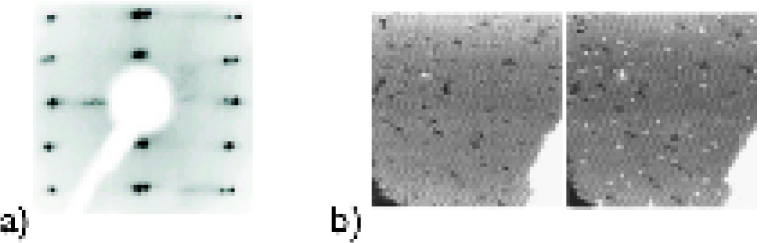
An example of LEED patterns is reported in Fig. 2.1.
Reflection High Energy Electron Diffraction (RHEED)
is also used, principally to monitor the thin film growth.
In this technique incident energies of keV
and incident angles of about degrees are used.
The structural analysis of LEED is often performed togheter with Auger Electron Spectroscopy (AES) to control the chemical composition of the sample. In AES a beam of electrons with energies beyond 1keV strikes the surface and the number of electron backscattered N(E) is analysed as a function of the energy. The gives the signature of the elements present in the sample.
Moreover we mention the light-ion Rutherford backscattering (RBS), where beams of H+ or He2+ ions are used with energies of hundreds of keV (LEIS up to 20 keV, MEIS from 20 eV to 200 keV and HEIS to 2 MeV). The ions are scattered by the nuclei of the crystal following the dynamics of classical Rutherford scattering and lose energy along straight trajectories through interaction with the electrons. Information on the composition and atomic displacements in the surface layers can be obtained thanks to this method detecting the number of ions as a function of the energy and the outcoming directions of ions diffused backward.
Another important technique employed to investigate the structural properties of semiconductors is Scanning Tunnel Microscopy (STM). Due to Binnig and Rohrer (1982), this technique gives the local density of occupied and empty states integrated over a given energy range around the Fermi level. This technique does not need UHV. An example of STM image is reported in Fig. 2.1.
From all these techniques we can get structural information about the system but a comprehensive interpretation of the data must usually be supported by a theoretical description which involves the knowledge of the electronic structure [29, 30].
2.1.2 Electronic properties
In translationally invariant systems the wave vector defines a set of good quantum numbers for each type of elementary excitation. In the case of an ordered surface of a crystal, such a wavevector , is restricted to two dimensions (parallel to the surface) because in the third direction the system is not translationally invariant anymore. The Surface Brillouin Zone (SBZ) becomes 2 dimensional and is defined as the smallest polygon in the 2D reciprocal space situated symmetrically with respect to a given lattice point (the origin) and bounded by points , satisfying the equation:
| (2.1) |
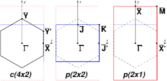
where is a surface reciprocal lattice vector. Figure 2.2 represents three of the five SBZ, referring to the ones we considered in the next chapters of this thesis: p-rectangular, c-rectangular and square. Further details on surface theory can be found in [28].
Among the experimental techniques which allow to inspect directly the band structure and the electronic structure in the 2 dimensional BZ we mention the most fundamental: Photoemission (PES), Angle–Resolved Photoemission (ARPES) and Inverse Photoemission (IPES).
PES is the most important technique able to give a picture of the Density of States (DOS) at the upper atomic planes. The physics behind the PES technique is an application of Einstein’s photoelectric effect. The sample is exposed to a beam of light inducing photoelectric ionization; synchrotron radiation is the ideal isochromatic radiation source. The energies of the emitted photoelectrons are characteristic of their original electronic states. For solids, photoelectrons can escape only from a depth of the order of nanometers, so that it is the surface layer which is mostly analyzed. PES can be performed with X-ray (XES), E20–150 eV, where it is possible to see transitions between surface bands below the edge of the bulk bandgap (the small cross section can be improved using grazing angles) [27].
ARPES gives information about the k-dispersion of bands and allows to separate the contributions from bulk and surface states. The former connect states with the same 3D -vector, the latter involve photoemission processes conserving only the component parallel to the surface . The detected 2D vector connecting surface states and the continuum can be written as:
| (2.2) |
where is a vector of the surface reciprocal lattice. Hence, plotting the electron energy as a function of the emission angle by:
| (2.3) |
we can say that the peaks in the energy distribution curve represent the initial state of the solid labelled by .
Inverse photoemission (IPES) allows to detect the energy of the photon emitted when an electron of an external beam of given E and falls into an empty conduction surface band or an image state. Even optical adsorption is a useful method to study the occupied and unoccupied states that in a first approximation can be described by the Joint Density of States (JDOS) defined by:
| (2.4) |
Finally STM is used to describe electronic states of the surfaces
by introducing a potential difference between the tip and the sample.In this way it is possible to have a spatial map of the wave function at different energies
for both empty and filled states (see Fig. 2.1).
In conclusion it is worth mentioning that spectroscopies which study
the electronic structure are also an indirect test of the surface atomic structure.
2.1.3 Reflectivity anisotropy experimental spectroscopy
Optical spectroscopy is an important tool to probe surfaces since
they allow for in situ, non–destructive and real–time
measurements. Moreover, material damage or contamination associated with
charged particle beams are avoided.
However, since the light penetration and wavelength are much larger than typical surface
thicknesses (few Å), optical spectroscopy is less sensitive to the surface.
Nevertheless, a trick can be used in order to resolve the surface signal. This is the case of Reflectivity Anisotropy Spectroscopy (RAS) and Surface Differential Reflectivity (SDR), optical techinques of great importance for detecting transitions between surface states. Surface sensitivity is greatly enhanced with the use of appropriate conditions which enhance the contribution of interband transitions involving surface states [33].
RAS is defined as the difference between the normalized reflectivities measured at normal incidence, for two orthogonal polarizations of light belonging to the surface plane:
| (2.5) | |||||
where R0 is the isotropic Fresnel reflectivity. Since the bulk of a cubic material is optically isotropic, any reflectivity anisotropy must be related to the reduced symmetry of the surface or to another symmetry breaking perturbation, for instance an electric field. In the case of we can write:
| (2.6) |
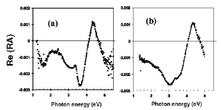
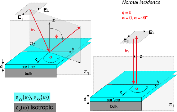
An example of measured RAS is represented in Fig. 2.3 and geometry scattering is shown in Fig. 2.6.
On the contrary an SDR spectrum is defined by the difference in the reflectivity measured on a clean surface before and after passivation (e.g. by adsorbing atoms or molecules on the surface). Passivation (oxidation, the case we discuss in chapter 5), removes surface states but does not affect bulk contributions. One hence obtains, for the optical response specific to the surface:
| (2.7) |
In conclusion, it is important to mention that all these techinques can be appreciably sensitive to the experimental definition of the surface in the sense that in some cases (e.g. Si(100) and Si(100):O, as treated in this work: see chapters LABEL:ch:si100,ch:oxi) the RA signal is modified because of the presence of steps, terrace or different oriented domains. The influence of steps on the reflectance spectra has been analysed by Jaloviar et al. [35]; hence Shioda and der Weide [36] use highly oriented surfaces (with terraces 1000 times larger than vicinal surfaces) in order to obtain more accurate RA profiles. Finally, a comparison of RA spectra obtained by nominal and vicinal surfaces is shown as an example in Fig. 2.3 where we reproduce data from Ref. [34] to illustrate how the use of nominal surfaces improves the spectral resolution in the low energy region of the spectrum.
2.1.4 Electron energy loss spectroscopy at surfaces
A natural complement to optical spectroscopy is
Electron Energy Loss Spectroscopy (EELS)
which, despite some complications in the interpretation
of the data, turns out to be surface sensitive probe,
particularly in High Resolution EELS (HREELS),
which uses low energy incoming beams.
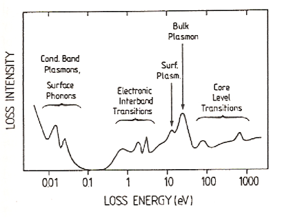
In an EEL experiment a material is exposed to a beam of electrons with a defined narrow range kinetic energy. Some of the electrons undergo inelastic scattering, losing part of their energy and having their paths slightly and randomly deflected from the specular direction. The amount of energy loss can be measured via an electron spectrometer and interpreted in terms of excitations of the sample. Inelastic interactions include phonon excitations, inter and intra-band transitions, plasmon excitations, and inner shell ionizations (see Fig. 2.4).
Usually EELS is performed in transmission, but to be surface sensitive it must be applied in a reflection geometry (REELS), see Fig. 2.7, and use relatively low incident energies (around 50–100 eV, versus 1 keV for bulk). In HREELS the beam is highly monochromatic and the energies of the electrons range up to few eV.
2.2 Theoretical surface spectroscopies
A real surface is a complex physical system
whose geometry, i.e. atomic positions, is generally unknown and
usually involve many degrees of freedom.
This makes calculations very heavy and can create
serious obstacles when fully treating excited states.
For this reason calculations are usually performed at different
levels of sophistication, involving various simplifications and
approximations, according to the accuracy required and the numerical
heaviness.
We assume to be able to calculate the dielectric tensor
of a general bulk system (as discussed in the previous chapters)
and we are going to describe how to use it in order to reproduce
and predict surface spectroscopic experiements.
2.2.1 The slab method
The description of the crystal termination is solved here using
the slab method, i.e. representing the surface by means of an atomic
slab of suitable thickness (usually 20-30 Å).
Using plane-wave basis sets, the three dimensional periodicity
of the system can be recovered by considering repeated slabs, separated by a
sufficiently large region of empty space.
In Figure 2.5 we illustrate the example of a slab inside
a supercell and indicate the three layers involved (giving
the name to the three layers model):
a bulk region (composed by the inner atoms of the slab),
a surface layer with thickness (top layers of the slab),
and a vacuum volume.
The thickness of the surface layer must be smaller than the wavelength
of the light.
The bulk properties are assumed to be described by an isotropic
dielectric function and the surface
is described by a frequency dependent dielectric tensor,
where the complex diagonal elements are defined by
, and .
In practical calculations, the vacuum region is chosen large enough to avoid the interaction between the two surfaces of the slab and careful convergence tests have to be performed. Figure 2.5 shows the case of a symmetric slab geometry describing an oxidised silicon surface. The slab method is general; also non symmetric slabs can be used, even if the case is not treated in this thesis.

2.2.2 Real–Space slicing technique
Within the description of the three-layers model, an electron impinging on the surface feels the potential from this surface layer through its dielectric function as well as the potential of the bulk region. However, microscopic calculations generally output the dielectric function of the supercell . In previous works [37], was extracted from by using the expression:
| (2.8) |
Here is the interlayer spacing, () is the number
of layers in each surface (bulk) region, and is the integral
of the slab RPA dielectric susceptibility
over and , i.e., . However
this approach cannot always guarantee perfect cancellation of the
bulklike layers in the supercell, and may even lead to unphysical
negative loss features.
A more reliable approach is to extract directly
using a real–space slicing technique, i.e. by projecting out
the response of a defined surface layer using a cut off function
in real space (for a detailed treatment see Ref. [38]).
This technique is usually reported in terms of the polarizibility
of the half slab , which,
in case of symmetric slabs, is obtained dividing by 2
the full polarizability :
| (2.9) |
where are the matrix elements of the
momentum operator222If the pseudopotential is
non local, is used instead of the momentum operator.
We introduce now a cutoff function aimed at projecting out
the optical transitions related to a certain selected region of the slab.
The function is a sum of two Heaviside step functions:
| (2.10) |
where is the thickness of the cutoff function (see Fig. 2.5).
The cutoff function is introduced into the calculation of the optical
properties through the use of a modified matrix element
, defined by:
| (2.11) |
and hence the polarizability of the slice is described by the relation:
| (2.12) |
In the next paragraphs we will show an application of this technique to analyse the layer-by-layer contribution of the electron energy loss spectra.
2.2.3 Theory of RAS
By exploiting a reflection geometry and the polarizability of the incident wavevector, certain spectroscopies are able to resolve the surface contribution to the optical properties of a material.
In the case of normal incidence light travelling from a first medium with to a second medium with (see Fig. 2.6) the Fresnel reflectivity is defined by :
| (2.13) |
where is the complex refraction index
.
Accordingly, reflectance is defined as a complex number for which
.
From the experimental point of view, measurements are usually performed
with respect to this quantity by:
| (2.14) |
On the contrary, reflectivity is a real number and with special cases occurring when (large difference between and ), () or when for the two media are both real or imaginary. Reflectance is a complex quantity linking the electric field amplitudes:
| (2.15) |
where , and hence . From Eq. 2.15 we can write:
| (2.16) |
from which we deduce that energy decreases exponentially.
If now we consider the energy density and
the absorption coefficient :
| (2.17) |
we obtain:
| (2.18) | |||||
| (2.19) | |||||
| (2.20) |
and finally
| (2.21) |
In the case of an interface with vacuum, the reflectivity is simplified:
| (2.22) |
In the case of non normal incidence (see Fig. 2.6) two contributions are distinguished:
| (2.23) | |||||
| (2.24) |
related to and waves respectively.
In experiments, the RA spectrum is calculated starting
from the knowledge of the reflectance and hence the reflectivity
by means of Eq. 2.5.
Theoretical models link reflectivity to the dielectric tensor.
In the particular case where ,
the relative deviation of the reflectivity with
respect to the Fresnel contribution is given in terms of the surface
and bulk dielectric tensor , by the equation:
| (2.25) |
representing SDRS formula in s-polarization, or, in the case of normal incidence:
| (2.26) |
In Eq. 2.26 we used the slab polarizability instead of the surface and bulk dielectric function. More details of this theory can be found in reference [33].
2.2.4 Theory of electron energy loss at surfaces
We use a semiclassical dipole scattering theory that accounts for the long-range interaction between the incident electrons and the medium under study [26, 39]. Assuming planar scattering, and taking as being the scattering plane ( is the surface normal, see Fig. 2.7) the scattering probability is defined by:
| (2.27) |
where and are the incident and scattered wavevectors respectively. The kinematic factor, A:
| (2.28) |
mostly contains the information concerning the scattering geometry
(see Fig. 2.7).

The angle is the direction of the incident
beam with respect to the normal to the surface plane, and
are the parallel and perpendicular components of the transferred
momentum .
The loss function is defined by:
| (2.29) |
and represents the part of Eq. 2.27 involving the approximation of the model and the separation between bulk and surface contributions to the dielectric function. If the surface were to be modelled as a semi-infinite truncated bulk, would be replaced by and we would obtain the familiar expression of Mills [39].
In this work we adopt an anisotropic three-layer model of the surface as derived by Selloni and Del Sole [40, 41]. The surface is modelled as in Fig. 2.8: a semi-infinite layer of vacuum, a surface layer of thickness , represented by the surface dielectric tensor , and a semi-infinite layer of bulk (dielectric function ). The effective dielectric function is defined by:
| (2.30) |
where is the thickness of the surface, and
are the bulk and surface dielectric function
and .
In particular and the auxiliary function
are written as a function of the
components of the dielectric tensor:
and .

|
Although the dielectric functions appearing in Eq. 2.30 are fully dependent
on and , such quantities are not easy to calculate, since and
are not independent.
Hence we make the approximation of replacing with the
optical dielectric function .
This appears to be a reasonable assumption since for most of the experiments modelled
in this work, is rather small.
Surface dielectric functions are calculated according to Ref. [38]
using a cutoff function (as discussed in the previous sections)
in order to select the number of terminal layers contributing to the
surface response.
Part II Development
Chapter 3 Efficient calculation of the electronic polarizability
In this section we show the application of an efficient numerical scheme to obtain the independent–particle dynamic polarizability matrix , a key quantity in modern ab initio excited state calculations. The method has been applied to the study of the optical response of a realistic oxidized silicon surface, including the effects of crystal local fields. The latter are shown to substantially increase the surface optical anisotropy in the energy range below the bulk bandgap. Our implementation in a large–scale ab initio computational code allows us to make a quantitative study of the CPU time scaling with respect to the system size, and demonstrates the real potential of the method for the study of excited states in large systems.
3.1 Motivations
The recent developments of experimental techniques for the non
destructive study of solid surfaces call for a simultaneous improvement
of the theoretical tools:
the interpretation and prediction of optical and dielectric
properties of surfaces require more and more quantitative and
reliable ab initio calculations, possibly including many–body effects.
Such an improvement of the theoretical description can be achieved, for example,
by lifting some of the usual approximations adopted in the calculation of
the optical response.
However, making less approximations increases the computational heaviness,
and is only possible if efficient numerical algorithms can be adopted.
A good example is given by the calculation of the independent–particles
dynamical polarizability matrix , which is
often required as the starting point in Time-Dependent Density
Functional Theory (TDDFT) [23] and in Many-Body Perturbation Theory-based
calculations, such as in the GW [42], or GW+Bethe-Salpeter
schemes (for a review, see e.g. ref. [3]).
Evaluating the full response matrix for realistic, many-atoms systems
can be computational challenging, since it requires a computational effort
growing as the fourth power of the number of atoms, and the availability
of efficient numerical schemes becomes a key issue.
Recently, schemes allowing to decouple the sum-over-states and the frequency
dependence have been presented. Miyake and Aryasetiawan [43]
and Shishkin and Kresse [44] have shown that methods based on the Hilbert
transform can substantially reduce the computational cost of frequency-dependent
response functions, making it comparable to that of the static case.
In particular the approach presented in [43] has been applied to a
linear-muffin-tin-orbital (LMTO) calculation of the spectral
function of bulk copper, while in [44], a work focused on the
GW implementation using the Projector Augmented-Wave method (PAW [45]),
a similar approach is used to compute the spectral function of bulk silicon
and materials with d electrons (GaAs and CdS).
Another recent work by D. Foerster [46] is focused on the same issue
and demonstrates how the use of a basis of local orbitals can reduce the
scaling of a susceptibility calculation for an N–atom system from to
operations for each frequency, but at the cost of disk space.
However, the application of such non-traditional
methods to large supercells, such as those involved in real
surface calculations, have not been presented so far.
It may be stressed that for a given application the computational burden is determined
not only by general scaling law, but also by prefactors.
In particular, prefactors determine the crossover where one method becomes
more convenient than the other.
This crossover has not yet been discussed for the Hilbert transform methods.
In the present work, we demonstrate the application of a scheme -similar to that introduced
in [43] and [44]- based on the efficient use of the Hilbert transforms,
by performing the calculation of the optical properties of a realistic,
reconstructed surface: Si(100)(22):O, covered with 1 monolayer (ML) of oxygen.
We provide a quantitative evaluation of the computational gain for this
calculation of the full dynamical independent-particle polarizability. The latter is constructed
from Kohn-Sham eigenvalues and eigenvectors and is then used to compute surface optical spectra,
including for the first time the local field (LF) effects on Reflectance Anisotropy (RAS)
and Surface Differential Reflectivity (SDR) spectra of this surface.
3.1.1 Local filed effects
The impact of local fields on surface optical spectra has been a controversial issue for decades,
specially concerning the so-called intrinsic or bulk–originated effects.
The latter have been measured, for energies above the bulk bandgap,
since the seminal works by Aspnes and
Studna [47] showing that the normal incidence optical reflectivity of natural
Si(110) and Ge(110) surfaces displays an anisotropy of the order of 10-3.
The effect was called intrinsic since it is not due to the existence of surface states,
nor to surface reconstruction.
Early model calculations by Mochan and Barrera [48]
performed for a lattice of polarizable entities and exploiting the Clausius-Mossotti relation
pointed out that intrinsic anisotropies could be due to LF effects. A subsequent
work by Del Sole, Mochan and Barrera [37] based on Tight Binding (TB)
method has shown that the RAS spectra calculated for Si(110):H within this semiempirical scheme did
not reproduce well the experimental data, despite the inclusion of surface LF effects.
However, more recent calculations based on realistic bandstructures
(within DFT-LDA with GW-corrected band gap) [49]
have suggested that intrinsic anisotropies at the bulk critical points for the
(almost ideally terminated) Si (110):H surface could arise as a consequence
of surface perturbation of bulk states, without invoking LF effects.
Other tight-binding calculations (see, e.g., ref. [50])
suggested the existence of intrinsic surface optical anisotropies not due
to surface local fields.
A substantial advance in clarifying the role of local fields has been achieved
only recently by F. Bechstedt and co-workers, who carried out a calculation of the
RAS spectra of Si(110):H [51] and monohydride Si(100)(2x1) [52]
including self-energy, crystal local fields, and excitonic effects from a
fully ab initio point of view.
In both the considered surfaces, which have no surface states within the bulk bandgap,
the LF were found to cause a slight decrease of the optical reflectivity; however,
the effect was found to cancel to a large extent in the RAS spectra,
being almost identical for the two polarizations of the incident light.
The situation may be different in the case of extrinsic optical anisotropies, i.e. those
directly related to surface states and surface reconstruction, and appearing
below the bulk bandgap. In at least one case
substantial effects due to LF have been reported [53].
However, further calculations for a wider class of surfaces are
necessary in order to assess this point more precisely.
The system we consider here belongs to a widely studied family of surfaces,
because of their importance in the understanding of silicon-silicon dioxide
interfaces in semiconductor technology.
Despite the many experimental
[54, 55, 56, 57, 58, 59, 60]
and theoretical
[61, 62, 63, 64, 65, 66]
works appeared in recent years,
the debate on the oxidation mechanism of Si(100) is still open.
However, the most favorable oxygen adsorption sites in the first stages of (room-temperature)
oxidation process have been identified as the dimer-bridge
position, and a bridge position on the backbond corresponding to the lower
atom of the dimer. This remark is supported by STM experiments [60] and by
a first-principles molecular dynamics calculation [66].
From the theoretical point of view, ground and excited state properties of
Si(100)(22):O at 0.5 and 1ML coverage have been recently studied by some of the
authors [67]; however, computational limits prevented till now the inclusion
of the local–field effects in the ab initio calculation of optical properties.
In the following paragraphs we brefly summarize
the theoretical framework and the expression
of usually employed in plane–wave based calculations.
Then we show how the Hilbert transform (HT) technique can be applied,
as a generalization of the Kramers–Kronig relations, in order to decouple
the sum-over-states and the frequency dependence in . Moreover
an estimation of the accuracy and the possible computational gain
are presented for a model system.
3.2 Theoretical framework
The starting point of our work is a DFT-LDA ground state calculation performed with
the ABINIT code [68] yielding independent-particle eigenvalues and eigenvectors
within the Kohn-Sham scheme [1, 2].
Besides to the occupied ones, empty (conduction) states up to an energy
of several eV above the Fermi level are obtained by means of iterative
diagonalization techniques.
However, in order to study the optical and dielectric response, the level of
theory must be brought beyond the ground state one, using, e.g.,
many–body perturbation theory or TDDFT [23].
The latter is particularly suited for the study of neutral excitations,
as those involved in optical reflectivity and electron energy-loss.
3.2.1 Fundamental ingredients
Within TDDFT, it is possible to obtain the retarded density-density response function from its non-interacting Kohn-Sham counterpart through a Dyson-like equation:
| (3.1) |
where the kernel contains two terms: the Coulomb potential, , and the exchange-correlation kernel, . An explicit expression for is then given by
| (3.2) |
Eq.s (3.1) and (3.2) are matrix equations, involving two-points functions such as and . In the present case, working within a plane-waves expansion, and are matrices in reciprocal space, and is the Coulomb potential. The exchange-correlation contribution, , is not exactly known. It can be included in an approximate form, e.g. using the LDA functional [5, 7] in the adiabatic approximation (ALDA), or in a more sophisticated approximation such as those described in [69, 70, 71, 72, 73, 74]. In order to compare with optical experiments, the macroscopic dielectric function must be calculated. The latter is defined as:
| (3.3) |
where the inverse dielectric function is linked to the response function by:
| (3.4) |
When only is included in the kernel of eq.(3.1) exchange and correlation effects in the response are neglected, while the use of the correct expression (3.3) still consider the LF effects [75]. Already at this level the calculations can become time consuming from the computational point of view when the full matrix has to be obtained. In complex systems with large unit cells the only tractable way to proceed is often to neglect local fields, by assuming that is well approximated by the average of the microscopic dielectric function:
| (3.5) |
This corresponds to neglecting the off-diagonal elements of in reciprocal space 111In real space, this corresponds to assume a dependence of only on the difference . When moreover exchange and correlation effects are neglected, (independent quasiparticle approximation or IP-RPA) the imaginary part of the macroscopic dielectric function takes the simple Ehrenreich and Cohen [76] form:
| (3.6) |
where is the velocity operator and i, j stand for occupied and unoccupied states respectively. The substantial simplification obtained in this case explains why most of the calculations of the optical properties of real surfaces are done within the independent quasiparticle approach, neglecting local–field effects. On the other hand, a fast and efficient scheme to compute the full matrix represents a key issue in order to be able to go beyond this approximation, e.g. by including the local fields, as we do in the present work. Moreover, an efficient method giving access to the full is of paramount importance when the screened coulomb interaction is needed, such as in ab-initio GW calculations. In the following, we hence concentrate on the expression of itself, i.e.:
| (3.7) | |||||
where are occupation numbers (0 or 1 in the present case), is an infinitesimal and the factor 2 is due to the spin degeneracy. Switching to reciprocal space and focusing on the case of semiconductors, we make valence (v) and conduction (c) bands to appear explicitly, and rewrite this equation as:
| (3.8) |
where is the volume of the unitary cell and we have also introduced the notation to indicate the Fourier transform of . From the numerical point of view the evaluation of these sums for each frequency can become very heavy. Indeed, for a realistic system the evaluation of eq. (3.8) involves, for each frequency, the summation over a large number of terms, which for a system of 50 atoms typically is of the order of .
3.2.2 The Hilbert-transform approach
Since we consider the case of the limit to study optical properties, in the following the label will be omitted to simplify the notation. The generalization to the case of finite q is straightforward. Introducing a simplified notation for band and -point indexes, we define a single index of transition t to represent the triplet . In this way, indicates an (always positive) energy difference, . We also introduce the two complex quantities:
| (3.9) | |||||
| (3.10) |
such that:
| (3.11) |
When (diagonal elements) the are real, and . Using
| (3.12) |
one can rewrite the limit of equation (3.11) as the sum of four terms:
| (3.13) | |||||
| (3.14) | |||||
| (3.15) | |||||
| (3.16) |
R and A label resonant and anti resonant contributions, respectively, and the four terms are general complex quantities. In and each term contributes to the function only at , and has no effect elsewhere. By discretizing the frequency axis, the sums over appearing in and can hence be performed once and for all, at difference with those labeled by R1 and A1 for which the sums should be calculated for each . Thanks to the linearity of the Hilbert transform, defined as
| (3.17) |
one can however directly obtain and from and :
| (3.18) | |||||
| (3.19) |
In such a way222In the case of real matrix elements, , one recovers the Kramers-Kronig relations linking real and imaginary parts of the response, it is possible to recover the complete in the spectral range of interest from the knowledge of a single sum performed over the poles . In other words, one can avoid the explicit summation over to be repeated for each frequency. The present procedure for the calculation of the frequency-dependent polarizability matrices is similar to the method of Miyake and Aryasetiawan [43], with the difference that those authors represented -functions using Gaussians, instead of bare rectangular functions as in our case 333Similarly, Shishkin and Kresse [44] used triangular functions.
3.2.3 Numerical efficiency for a toy system
Our scheme has been first tested on a model system444We considered
bulk silicon Kohn-Sham energies, increasing the number of transitions to build ,
and randomly redefining the transition matrix elements in order to check both the accuracy and the efficiency of the
algorithm. Figure (3.2) shows the results of the test,
comparing (real part) as obtained in the traditional
way (i.e. by evaluating expression (3.8)
for several frequencies), and by the Hilbert transform (HT) algorithm.
The results are practically indistinguishable on the scale of the plot.
The same figure shows the growth of the required CPU time as
a function of the number of transitions (number of triplets).
The gain appears to be proportional to the system size.
The possibility to achieve such a large gain, at least in principle and for
a simple system, was also noticed in the previous works describing
efficient algorithms for the calculation of [43, 44].
Alternative approaches for efficient TDDFT calculations have also been suggested.
In particular, another promising scheme based on a superoperator approach and
allowing to access TDDFT spectra in a numerically efficient way has been
recently introduced by Walker and coworkers [77].
This approach is however not designed for the calculation of the
whole matrix , contrary to the method studied here.

In order to know the actual CPU requirements for the calculation of , and to
explore the possibilities to study complex systems, such as the impurity levels and
band offsets mentioned in ref. [44], in practice one has to keep into account
the time used to compute the matrix elements (numerators in eq. 3.11),
and the time used to perform the Hilbert transforms, which was not explicitly evaluated in previous works. In
the following, we hence applied our approach, similar in its essence
to that used in [43] and [44], to a large system investigating the actual
numerical performances of the algorithm. As it will be shown below, substantial improvements
can actually be achieved in such realistic calculations.

Therefore, in the following section, we use our implementation
of the HT scheme in the ab initio DP code [78]
to study a real reconstructed surface: the oxidized Si(100)-(22),
for which we present the first calculation of its optical reflectivity spectra
(RAS and SDR) with the inclusion of local–field effects.
Finally, we carefully compare the numerical performance of the
DP code with and without the use of HTs, and we draw our conclusions.
3.3 Optical properties of oxidized Si(100)-(22)
The HT method has been implemented into the large scale, plane–waves ab initio TDDFT code named DP, developed by the French node of ETSF [79]. As mentioned in the previous paragraphs, we used it to calculate the optical properties of Si(100)(22):O. For this surface we adopt the equilibrium structure for 1ML coverage shown in figure (3.4), which is representative of a situation in which dimer and backbond sites are both occupied by an oxygen atom (structure c3 in ref. [80, 81] and see chapter 5 for further considerations). The surface is simulated with a slab composed by 6 layers, containing 48 Si and 8 oxygen atoms, in a repeated supercell approach. Our structural results agree well with those of previous calculations [62, 82, 80, 81]. We use standard norm conserving pseudopotentials of the Hamann type [21], and an energy cut off of 30 Ry, yielding 15000 plane waves in our unit cell. Eight special (Monkhorst-Pack, [83]) -points in the irreducible Brillouin zone (IBZ) are used for the self-consistent ground state calculation, while a 77 grid is used in the evaluation of . Kohn-Sham eigenvalues and eigenvectors are obtained for all occupied states (120) and for empty states up to 15 eV above the highest occupied state (top valence). Optical properties are computed through the evaluation of the macroscopic dielectric function with and without the inclusion of local field effects.
![[Uncaptioned image]](/html/1211.6270/assets/x12.png)
![[Uncaptioned image]](/html/1211.6270/assets/x13.png)

Figure 3.3 shows the imaginary part of the slab dielectric function as a function of the energy. Local–field effects are quite important in the low energy region (0-2)eV, enhancing for light polarized along the direction of the dimers chains (x direction, see Figure 3.4), and suppressing it for light polarized along the dimers axis (y direction). This goes in the direction of a better description of the microscopic inhomogeneities of the system. In the present case, the extrinsic surface optical anisotropy, as defined in the introduction, is hence found to be visibly affected by LF. In the case of the third polarization, i.e. the one perpendicular to the surface (not experimentally relevant in the case of normally incident light), local–field effects are huge, and introduce a blueshift of the absorption edge as large as 5 eV. This can be explained by the strong inhomogeneity of the charge distribution in passing from the slab to the vacuum, leading to a classical depolarization effect. Similar behaviors have been found for example in GaAs/AlAs superlattices [84], in graphite [85] and nanowires [86, 87].
Starting from the slab dielectric function, we computed Reflectance Anisotropy (RAS) and Surface Differential Reflectivity (SDR) Spectra [88], with and without inclusion of LF effects. We used theoretical models (see chapter 2 or [33]) linking the RAS and SDR spectra to the dielectric functions evaluated for the bulk crystal () and for the slab () through the relation:
| (3.20) |
where and are the diagonal components of the surface dielectric tensor. We show our results for RAS and SDR in figures 4.9 and 3.6 respectively.


We first discuss the case of RAS. The effects of local fields on the imaginary part of the dielectric tensor are most evident in the low-energy region of the spectrum (below 2 eV), as shown in the inset of Figures 3.3a and 3.3b. In particular, LF are found to enhance and sharpen the strong peak at about 1.2eV for light polarized along the dimer chains (fig. 3.3b), and to reduce the first three peaks for light polarized along the dimer axis. As a result, LF induce a strong enhancement in the surface optical anisotropy (of the order of 100%) in the region between 0.8eV and 2eV, as displayed in fig. 4.9. This low-energy region (below the direct gap of bulk Si) corresponds to surface-localized states, which are expected to carry the surface anisotropy. The fact that LF evidence this anisotropy is consistent with the fact that dimer chains realize a structure which is geometrically strongly inhomogeneous in the direction perpendicular to the dimer chains (see fig. 3.4). At higher energies (above 2eV) bulk contributions dominate , and the resulting RAS is mainly due to surface perturbed bulk states. The latter appear to be less affected by local fields than the true surface states, and lead to a RAS spectrum which, above 2.0eV, is almost insensitive to the inclusion of local field effects. This picture is confirmed by the analysis of SDR results. The latter are in fact calculated for unpolarized light, i.e. by averaging and . Since LF enlarge and reduce , their effects almost completely cancel out when the average is taken. Our calculated (unpolarized) SDR spectrum, displayed in fig. 3.6, appears in fact to be very little affected by the local fields, in the whole energy range between 0 and 6 eV. However, if a polarized SDR spectrum is computed, then local fields are found to influence the low-energy region (eV), in a way which is very similar to the behavior of the RAS.
Unfortunately, it is not possible to perform here a comprehensive comparison with RAS and SDR experimental data, since this would require the calculation of several possible reconstruction and geometries. In fact, the oxidation mechanism of Si(100) has been shown to be exceedingly complex, with different mechanisms playing their role depending on the oxidation temperature: a barrierless oxidation of the first Si layer [66], or an “active oxidation” involving etching of the surface and penetration of oxygen in a layer-by-layer manner at higher temperature [89, 90, 91]. Recently, the Si(100)(2x1):O surface optical anisotropy has been shown to be sensitive to the structural details of the oxygen adsorption by ab–initio calculations of the atomic geometries and optical response of a large number of Si(100):O structures [92, 93]. An highly structured potential energy surface has been found, with minima at the backbonds of the “down” atoms in Si–Si dimers [93]. Moreover, an appreciable amount of disorder is probably present after oxidation of the first Si monolayer, and the local strain induced by oxygen adsorption is expected to have a sizable impact on the optical anisotropy spectra [92].
However, our findings for LF effects in the single case studied here suggest an important general remark about surface optical spectroscopies. In fact, it is well known that, due to the large penetration depth of visible and UV photons, the surface–specific optical reflectivity signal is very small with respect to the bulk contribution. For materials with an isotropic bulk, the RAS spectroscopy has indeed been developed in order to extract the surface signal, by exploiting its anisotropy. A correct evaluation of the latter has hence the highest priority in theoretical calculations of surface optical spectra. The fact that crystal local fields are potentially able to alter significantly the surface optical anisotropy, at least below the bulk bandgap, should hence be kept in mind, particularly when the anisotropy of electronic states is associated with a large structural anisotropy at the surface, such as in the case of dimer chains on Si(100)(21).
3.4 Computational scaling and performances
In this section, we present a quantitative analysis of the numerical performance of the HT-based approach, as implemented in the large scale code DP [78], with respect to the traditional approach. Several calculations have been done by varying the three main convergence parameters: (i) the number of valence–conduction transitions (); (ii) the number of frequency intervals considered in the spectrum, i.e. the spectral resolution (number of frequencies, ); (iii) the number of plane–waves considered in the response matrix (). Optical properties usually converge at an value which can be substantially smaller than the total number of plane waves, , used to describe the wavefunctions.
The calculation of is expected to scale, in the case of the reference approach, as 555 leads to the scaling mentioned in the introductory section.:
| (3.21) |
where is the number of k-points, and and are prefactors which are independent on , and . The first term in equation (3.21) is due to the evaluation of the numerators in equations (3.14) and (3.16) by using FFT, and is present both in the reference and Hilbert approach. The second term stems from to the evaluation of equation (3.11) in the traditional way. The remaining term A keeps into account residual parts of the calculation, as the matrix inversions, which contribute much less to the CPU time than the first two terms.
The expected scaling in the case of the Hilbert-based scheme is instead:
| (3.22) |
In this case, the second term does not contain the factor anymore, and its prefactor becomes , due to the calculation of and (equations 3.14 and 3.16). The calculation becomes, in this sense, comparable to a static one.
However, the actual evaluation of the Hilbert transforms (equations 3.18 and 3.19) introduces a new term scaling as . Due to the small prefactor , the latter term can often be neglected (see, e.g., figure 3 of reference [43]). In the present work, we found that the CPU time spent inside the Hilbert transform itself can be made negligible by an optimized algorithm666Exploiting the fact that the principal value numerical integration routine has to be called times, always on the same energy intervals, a substantial gain could be achieved by tabulating the (about ) required values of the complex logarithm once and for all at the beginning of the double loop over the number of vectors in the construction of ..


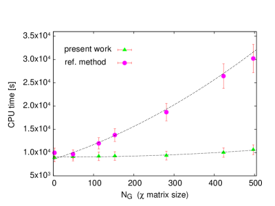
Considering an N-atoms unit cell, the number of transitions is clearly the parameter growing fastest with the system size, since it is proportional to N2. About 22000 transitions per -point, corresponding to the inclusion of about 200 empty bands, are requested to converge the dielectric tensor of the Si(100)(2x2):O slab up to 12 eV. The number of frequency intervals, , is instead independent on N, but it grows linearly with the required spectral resolution. In the present case, 300 frequencies have been necessary in order to achieve a 40 meV resolution over a spectral range of 12 eV. Finally, , i.e. the size of in reciprocal space, depends on the requested real-space resolution needed in the description of the induced density variations. This means that larger will be necessary to describe systems with smaller interatomic distances, or with larger polarizability. The real-space resolution is independent on the system size; however, for a fixed resolution will grow linearly with the volume of the unit cell in direct space. is hence proportional to the number of atoms (in a bulk system) or to the volume of the supercell (for a finite or semiinfinite system). In our slab calculation, converging the spectra with local field effects requires to consider at least 113x113 matrices (incidentally, we stress that the IP-RPA spectra, requiring just the , matrix element of , do not depend on ).
The HT algorithm turns out to be clearly advantageous with respect to and , as shown in the first and last panels of figure 3.7. Concerning , despite an unfavorable scaling in the limit of infinite spectral resolution (the CPU time grows quadratically with the number of frequency intervals), one must notice that, due to the small prefactor , the HT method is largely convenient in whole range of interest ().
3.5 Conclusions
Two classes of conclusions can be drawn from the presented results. First, the physics: the study of Si(100)(2x2):O has shown that local field effects, although playing only a minor role on the surface optical properties above the bulk bandgap, are able to enhance substantially the surface optical anisotropy in the low–energy end of the spectra. A similar effect can be expected for other surfaces, when the anisotropy of electronic states is associated with a large structural anisotropy, such as in the case of the dimer chains on Si(100)(2x2). Moreover, large local field effects are found for light polarized normally to the surface. Second, the numerics: the computational gain achievable by using the Hilbert transform-based algorithm has been shown to be substantial, both in a model system and in a real, physical application. A successful implementation of the Hilbert transform method in the large-scale plane-waves ab initio computer code DP [78] allows us to locate the crossover (starting from which the Hilbert transform algorithm becomes convenient) already at medium size systems (less than 50 atoms).
Part III Applications
Chapter 4 The clean Si(100) surface
Surfaces are complex physical systems that are very important from both the fundamental and technological point of view. One of the most important surfaces of all is the (100) surface of silicon, as it appears in most electronic devices. Nevertheless, in spite of its many applications, a completely unambiguous structural and physical description of Si(100) is lacking. In this chapter we summarize our results about first principles calculations of electron energy loss spectra of the Si(100) clean surface.
4.1 Si(100): which reconstruction?
Due to its enormous technological importance, the Si(100) surface has been the
subject of a wide range of experimental and theoretical studies spanning several decades.
In fact, quality publications continue to appear
regarding the atomic structure and electronic properties of the clean surface.
Following early LEED experiments [94], it was understood that Si(100)
forms a reconstruction. The classic explanation of the LEED observation
is that the surface is composed of rows of Si dimers separated by trenches
(Fig. 4.2), as confirmed by various scanning
tunnelling microscopy studies [95, 96].
Although some quantum chemistry studies have found that a symmetric dimer
structure (causing a metallic surface) forms the global
minimum [97],
several total energy calculations based on density functional
theory [98] have found that dimer buckling
induces a small energy gain, such that the dimers adopt an asymmetric configuration
and the surface remains semiconducting [99].
Three distinct structures have been proposed for the Si(100) surface: the ,
whereby all dimers are buckled the same way (see Fig. 4.2(a));
the structure, where alternating dimers in a row are buckled in
opposite directions, and adjacent rows are buckled in phase
(see Fig. 4.2(b));
the phase, being the same as the but with adjacent rows
buckled out of phase (see Fig. 4.2(c)).
Total energy calculations have found [98]
that the reconstruction is prohibitively higher in energy
than the other two (at zero K), and that the is only slightly
favoured over the .
Which reconstruction occurs on the surface depends critically on the temperature.
LEED studies have shown that an order-disorder phase transition occurs at about
200K [100, 101].
Below this critical temperature, a phase is generally observed; above it,
a periodicity is seen.
Direct observation of the surface structure with STM is complicated by two factors however.
Firstly, it is well established now that the experimental measurement itself
can influence the result, and drive phase
transitions [102, 103].
Charge injection, or electric fields induced by the STM tip, can cause dimers to
flip, according to various
experimental [104, 103]
and theoretical works [105, 106].
Nevertheless, the general consensus is that the reconstruction is the more
stable structure below the critical temperature [103, 107].
Above 200K, STM images appear to show a symmetric dimer configuration.
However, at these temperatures the dimer rocking mode is activated,
and hence it is believed that the observed symmetric structure is merely a time average
of the thermal flip-flop motion of the buckled dimers.
Based on molecular dynamics simulation of the dimer motion, it was suggested that
the surface consists of simultaneous local presence of asymmetric dimers, and
of instantaneously flat symmetric dimers [108].
More recent studies have suggested that the dimers remain short-range correlated
(see refs. 32–35 in Ref. [109]).
In particular, a two photon photoemission (2PPE) study found minor difference
between the surface band dispersion at 90K and at room temperature [110].
Theoretical simulations of the reflectance anisotropy (RA) spectra
confirm that the reconstruction does not reproduce correctly the
experimental lineshape [111, 112, 113].
On the other hand, both and structures
are quite similar to the experiment, with the yielding a slightly
better agreement [111], in particular predicting
the observed SDR structure below 1 eV.
Simulation of the surface differential reflectance also favours the surface [114].
In addition to optical techniques such as RAS or SDR,
electron energy loss spectroscopy (EELS) in the reflection geometry (REELS or RELS)
offers an enhanced surface sensitivity and easy access to a wide energy range
(see chapter 2).
Although the majority of literature considering REELS of Si(100)
has focused on vibrational properties [39],
several studies have examined the nature of electronic states
at the clean Si(100) surface [115].
Indirect information about surface states was derived from
related studies looking at the changes in the REEL spectrum following
oxidation [116, 117, 118].
High resolution (HREELS) measurements were carried out by Farrell et al. [119]
and Gavioli et al. [120].
In the latter work, tight binding calculations were performed on the symmetric
and asymmetric dimer models, and suggested that a mixture of the two structures
was necessary to explain the room temperature EEL spectra.
However, the structure was not considered in that work, and therefore some
of the conclusions reached are not complete.
In the following sections, we present a computational study of high resolution EELS
for the different reconstructions of Si(100): , and Ẇe consider the energy range that probes the excitation of
interband, i.e., about 0–6 eV, and hence
connect the experimental observation directly with the atomic structure and
microscopic electronic response.
4.2 First principle scheme
We use density-functional theory within the local density approxiation (DFT-LDA),
within a plane-wave and pseudopotential framework.
The ABINIT [121, 122] and
quantum-espresso/PWSCF [123]
codes were used for computing the relaxed atomic structures, electronic bandstructures, and
Kohn-Sham eigenvalues and eigenvectors required for the evaluation of the
optical properties.
However, in order to be consistent and since we found only minor differences between spectra computed with the
two codes, we report only the final results obtained using the output of PWSCF.
For all our calculations we used standard norm conserving pseudopotentials
of the Hamann type [21] for both silicon and oxygen
generated with FHI98PP package [124] within DFT-LDA
(Perdew-Zunger parametrization [7]) framework.
4.3 Geometric structure
Even if a 7.5 Ha kinetic energy cutoff is rasonable in order to treat the case of a clean silicon surface, we used a 15 Ha cutoff throughout, as was previously found to be sufficient for oxidized Si(100) with the same pseudopotential [67]. The effect of the two cutoff is shown in Fig. 4.1 where it is clear that the minimum of the curve is not appreciably different.

Therefore we used the theoretical lattice constant of 5.393 Å,
as determined at 15 Ha A standard repeated-slab and supercell approach was adopted in order to model the surface
structure.

We use relatively thick slabs (16 atomic layers) separated by 8 layers of vacuum (about 10 Å).
During the geometry optimization, the central four layers were fixed at the bulk positions and
structures were relaxed until the cartesian force components were less than 20 meV/Å. Our obtained structural parameters are similar to those obtained previously for this surface (see
for example Ref. [111])
such as a dimer buckling of 0.755 Å and a dimer length of 2.33 Å.
4.4 Computational aspect
Optical spectra and energy loss spectra were calculated using the YAMBO code [125], taking Kohn-Sham eigenvalues and eigenvectors from a non-self-consistent run of the PWSCF code [123]. We carried out convergence tests on the optical and energy loss properties with respect to the number of bands and the number of -points. For the calculation of energy loss we included up to 320 unoccupied bands, corresponding to minimum – transition energy of eV.

Further convergence tests were carried out
regarding -point sampling. For the most converged calculations, we used
roughly equivalent density sets for the three reconstructions:
for the , 72 -points in the irreducible Brillouin zone (IBZ),
which is equivalent to 1152 points in the BZ
(for both clean and oxidized cells, see next chapter);
for the , 64 -points in the IBZ
(equivalent to 1024 points in the BZ);
for the , 100 -points in the IBZ
(equivalent to 800 points in the BZ).
All spectra reported in this work were obtained using the non-interacting particle (RPA) level
of theory. Many-body effects, including local field and excitonic effects, were compensated for
by applying a scissors operator of eV to the unoccupied states, following the recipe of
Del Sole and Girlanda [37].
In this way we account for the well-known underestimation of
the DFT band-gap, and partially include self-energy and excitonic shifts in energy.
The value of eV was determined in other works on Si(100) as giving best agreement with the
experimental RAS [67].
In the following subsection we present some discussion of major technical
tools used in order to compute REELS.
4.4.1 Broadening
Inspection of Eq. 2.28 reveals that the cross section goes as as . Hence any features appearing in the loss function Im at low energy can be dramatically enhanced by the kinematic factor. From the computational point of view this means that unphysical features may appear close to the origin if a Lorentzian broadening is used when calculating the surface dielectric function of a system with a small band gap. We adopt therefore a tiny Lorentzian broadening of eV when calculating the dielectric function, and afterwards convolute the loss spectra with a Gaussian (FWHM = 0.3 eV) to approach the experimental resolution.


4.4.2 Slicing methods
A crucial adjustable parameter present within the three-layer model of energy loss is the thickness of the surface layer, as used in Eq. 2.30. According to the model, an electron impinging on the surface feels the potential from this surface layer through its dielectric function as well as that of the bulk layer . Obtaining from the dielectric function of the slab or supercell is not trivial. However early efforts used a simple subtraction of the computed bulk dielectric function [37]:
| (4.1) |
where I is the integral of the slab RPA dielectric susceptibility over z and z’, is the interlayer spacing, Ns is the number of layers at each surface with dielectric function and Nb is the number of inner layers with bulk dielectric constant . Unfortunatly this approach cannot always guarantee perfect cancellation of the bulklike layers in the supercell, and may lead to unphysical negative loss features.

A better approach is to extract directly using a “cut off” function as described in chapter 2 or in Ref. [38]. Nevertheless, the choice of remains somewhat arbitrary. In this work we define the lower bound of the surface layer corresponding to the actual penetration depth of the electron for the chosen incident kinetic energy, with the upper bound defined by the maximum extent of the slab charge density or a typical surface state wavefunction (see Fig. 4.5). This turns out to be roughly one atomic layer. We then checked that varying by an atomic layer did not change the results too much. The dependence of the REEL spectra on the parameter is illustrated in Fig. 4.5.
4.4.3 Detector integration
In experimental EEL spectroscopy the detector has a finite acceptance angle for collecting the scattered electrons. Hence, in order to improve the quantitative estimation of the EEL spectra at the surface, we implemented a method to perform a numerical integration over the circular detector. In particular we account better for the finite size of the detector window through a random sampling of the circular area and in the computation of the following integral:
| (4.2) |
We implemented the method in the Yambo code [126], the code we used for all further calculations.

In Fig. 4.7 an illustration of the importance of numerical detector integration scheme with regard to relative intensity of peaks is shown.
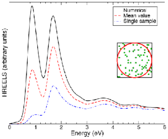

A frequently used technique is to approximate the integral by an averaged value of the transferred momentum .
A comparaison between the two methods is shown in figure 4.7 where relative intensity of the low energy peaks is corrected with converged numerical integration. We also add a figure showing the effect of the detector size on the EEL spectrum.
4.5 Calculated spectra for Si(100)
A review of the current understanding of the structure of the clean Si(100) surface was given in the introduction and a schematic diagram of the three basic surface reconstructions (the , and ) is given in Fig. 4.2. Throughout this work we will refer to the direction as and the direction as , with being the surface normal . Here we present our results concerning optical and electronic spectroscopic study of the clean Si(100) surface.
4.5.1 Reflectivity anisotropy spectra
Several theoretical studies of the RA spectra for the Si(100) surface have previously
been carried out, including tight binding calculations [127],
discrete-dipole models [128, 129],
ab initio calculations at the independent particle
level [130, 131, 132, 114, 67, 112, 113]
as well as more recent studies including many-body effects [133].
Generally it was found that the best agreement with the experimental RA
data [36]
is obtained when the or models are used in the calculations,
while the gives poor agreement.
Since we will use the same optical dielectric functions when computing the
energy loss spectra, we show for completeness (in Fig. 4.9)
the results of our own supercell calculations
for the , and reconstructions
at the independent particle level.
The reflectance anistropy (see chapter 2) is defined as
| (4.3) |
where () is the normalized reflectivity
(i.e., relative to the Fresnel reflectivity).
As expected, we find that both and spectra
yield a good agreement with the experimental data.
The reproduces the low energy peak at 1.5 eV rather well,
but the comparison worsens at higher energy. Unfortunately, no experimental
data is available for the RAS of Si(100) in the near-IR range, and is hence limited
to 1.1 eV.

4.5.2 Calculated REELS spectra at 40 eV
We now contrast the RAS results with the theoretical simulation of the HREELS experiment
of Farrell et al. [119] with incident
energy of eV, which roughly covers the same spectral range as
the available RAS data.
Experimental results refers to specular geometry with incident angle of .
There exists a one-to-one correspondence between RAS and HREELS
that can be justified with theoretical arguemnts when
we consider a spectral range below .
In fact it can be written that RAS is proportional to
Im when Im is close to zero.
On the other hand:
| (4.4) |
giving a direct proportionality of REEL respect to .
This correspondence is evident in Fig. 4.14 where
HREEL peaks and Im are represented.
The experimental one-to-one correspondance between RAS and HREELS was also
previously illustrated by Arciprete et al. [134]
for the case of GaAs(001)-.
The experimental data, which are reproduced in Fig. 4.10, are
characterized by surface-derived soulder at 0.9 eV () and a broad peak
at 1.4-2.0 eV (),
and bulk-derived peaks at about 3.5 eV and 5 eV.
The latter peaks have also been identified in second-derivative
off specular geometry spectra at =100eV by
Rowe and Ibach [115]
as deriving from the bulk critical points, and .
In the experimental spectrum of Fig. 4.10 we have
subtracted a background signal, taken to be that of the monohydride
Si(100)-:H surface, also reported in Ref. [119].
The results of our first principles calculations of HREELS are shown in Fig. 4.10
for the , and reconstructions of Si(100).
From the comparison with experiment it is clear that the alone
cannot reproduce the experimental signal since the shoulder at 0.8 eV ()
is missing from its theoretical spectrum.
A similar observation was made by Gavioli et al. [120]
based on tight binding calculations of the HREEL spectrum.
Moreover we observe that, as in the case of the RAS, it is difficult to distinguish
between the and calculations.
The peak appears at a slightly lower energy (by 0.1 eV) in the
calculation; however, considering the approximations used in the present calculations
(scissors shift), it is not sufficient to allow us to prefer the
over the .
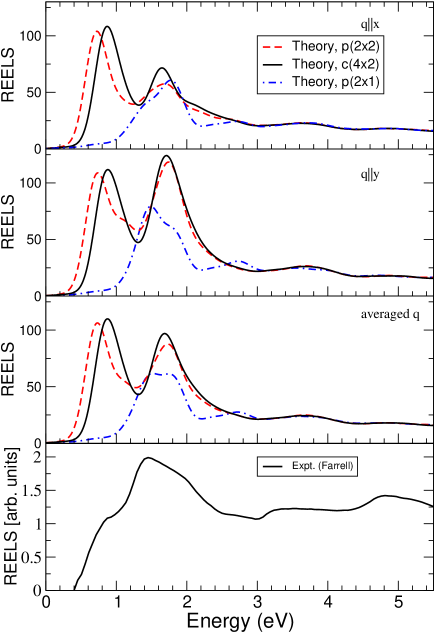
As discussed in Section 2.2.4, the three-layer model of energy loss
is based on the assumption that the electron does not penetrate the surface,
so that losses occur from scattering off long range potentials above the surface.
In reality, electrons with a 40 eV kinetic energy actually penetrate the surface by
several atomic layers before elastic scattering occurs.
As a result, features in the loss which arise from scattering within the crystal itself
(as occurs naturally in transmission EELS) are missing from our theory.
Hence the calculated lineshape differs significantly from the experimental
one above 2.5 eV.
To counteract this deficiency of the theory, we augment the reflection loss term with a second loss term that represents the trasmission loss, or “bulk” loss within the subsurface layers:
| (4.5) |
The result is shown in Fig. 4.11. Since the three-layer model already accounts well for losses in the surface layer (the spectra presented here actually do not change much if a loss function of the form is used), we find we only need to increase the proportion of bulklike losses below the surface to improve the agreement with experiment.
In spite of the agreement reached it is clear from the relative intensity of the and peaks that one single reconstruction cannot reproduce the experimental spectra.
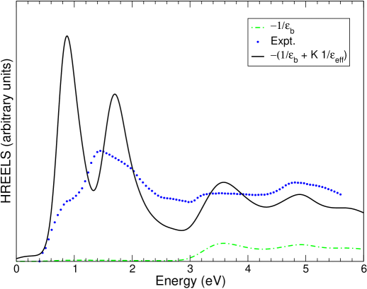
4.5.3 Calculated REELS spectra at low energy
Although many REEL spectra are present in the literature that study the
Si(100) surface, only a few high resolution spectra
that probe the interband transitions of Si(100) are available.

We reproduce in Fig. 4.12 the HREELS data for low-energy incident
electrons reported by Farrell et al. [119]
( 7 eV; specular scattering; probably at T=300K)
and Gavioli et al. [120]
(for a slightly different experimental setup: 6.8 eV;
; T=120–500K).
In both works, two main structures are identified in the spectra below 2 eV.
Farrell reports an adsorption edge at 0.4 eV with a peak at 0.75 eV
(termed ), and a second edge at 1.1 eV with a peak at 1.65 eV
(termed ).
We note that the peak was identified by Farrell as being the peak observed by
Ibach and Rowe [115, 117]
at eV and by Maruno et al. [135] at about 2.0 eV.
In the more recent work by Gavioli et al., various HREELS data were
reported at temperatures ranging from 120 to 300 K,
and at different analyzer focalizations (see Fig. 4.12).
At low temperature a shoulder is found at 0.68 eV,
as well as two main structures at 0.9 eV and 1.15–1.35 eV.
It is not clear, however, if the latter feature corresponds
to the structures reported elsewhere, as any peaks appearing
at around 1.7 eV in Gavioli’s data seem to be obscured by the background noise.
Note that the main low energy peak occuring in the RAS is at 1.6 eV,
as seen in Fig. 4.9, which would appear to agree with
the peak positions of Farrell et al..
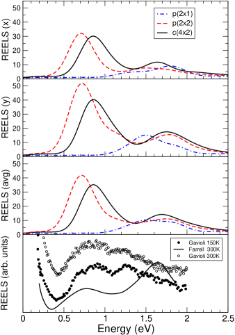 |
 |
In Fig. 4.13 we report the results of our ab initio simulation of this HREELS experiment. As noted for the eV data, it is clear that the model does not yield the correct lineshape, as the peak is missing. Both and structures succeed in reproducing the double-peaked structure observed in the experiments. In particular, the peak is well reproduced by the model, and it is possible that the shoulder observed at 0.68 eV points to the coexistence of some on the predominantly surface. The calculated energetic position of the peak is in reasonable agreement with the data of Farrell, but not so much with that of Gavioli. However, it is worth to mention that Farrell’s data beyond 1.5 eV can be affected to background and are not completly relible because some fit of experimental data has been performed and in the original paper the dashed line at that energies give us some doubts on the exact position of that peak. For this reason we feel more confident in the more recent Gavioli’s data.
4.5.4 Analysis of spectra
In the following two sections we concern ourselves with interpreting the experimental peaks observed in the HREEL spectra below 3 eV for the kinematic setup of Farrell and Gavioli at eV.
Fig. 4.14 compares the calculated surface dielectric function
with the calculated HREEL spectra.
It is clear that there is a one-to-one correspondance between peaks
in the energy loss and peaks in the imaginary part of the dielectric function.
Hence we can analyse to characterize peaks in the HREEL spectra.
The experimental spectra feature two main peaks, termed and in the literature [119]. The microscopic origins of these peaks is now analysed for the reconstruction. Figures 4.15 and 4.16 show the total oscillator strength , as a function of , corresponding to an energy window of width centred around a chosen peak energy :
| for |
It is clear that arises from transitions located around the point for both polarizations (see Fig. 4.15) On the contrary arises mostly from transitions along – direction.
The location of these transitions with respect to the surface band structure is shown in Fig. 4.18. Our bandstructure calculation for the clean surface compares well with that previously published by Fuchs [113]. In particular, a surface state is present at about 0.8 eV above the valence band maximum.
Finally, we looked at for the valence and conduction band states taking part in the strongest transitions. These are plotted in Fig. 4.17 using Xcrysden package [136]. We found that derives from transitions between surface states: dangling bonds and -hydridized orbitals, or to orbitals as shown on Fig. 4.17. To have a confirmation of this statement an analysis of Fig. 4.16 and of the band structure (top of Fig. 4.18) is required. In fact, Fig.4.16 shows that the most part of transitions contributing to comes from k points along – path in the SBZ and the band structure clarify which bands are involved. In fact, looking at the band structure in Fig. 4.18 it is clear that S1 peak comes from transitions between the flat bands in the – direction (blue arrows).
On the other hand, is due to transitions between bulk states at the valence band maximum (in ) and unoccupied surface states within the fundamental bulk bandgap. A representative pair of states involved in this kind of excitation is shown in Fig. 4.17 (top). Moreover, with a similar analysis as done for , band structure and Fig. 4.15 (red arrow) give a confirmation of the fact that is more symetric involving transitions around the point.
 |
 |
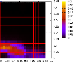 |
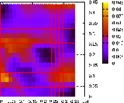 |
||
 |
 |
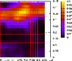 |
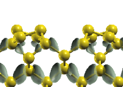 |
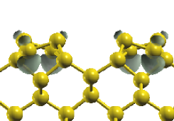 |
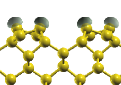 |
 |
4.5.5 Discussion
We now show how our HREELS calculations can be used to better understand the structure of the Si(100) surface as a function of temperature. Si(100) exhibits a LEED pattern above the order–disorder transition temperature of about 200K. Our findings (Fig. 4.13)—that the surface alone model cannot reproduce the experimental HREELS data—are consistent with current understanding of the surface at this temperature (rapid dimer flipping). At lower temperatures, the surface should be predominantly .
The experimental dependence of the HREEL spectra of Si(100) was studied by
Gavioli et al. [120], and their results are reproduced
in Fig. 4.12.
In that work, the observed spectrum was explained as being due to a mixture of
symmetric and asymmetric structures. However, there is much
evidence to show that symmetric dimers do not exist at 150K.
Furthermore, they did not consider the structural model, which we find
is sufficient to produce a double-peaked HREEL spectrum (Fig. 4.13
and 4.10).
Increasing the temperature, the peak is found to decrease by 5% and
the peak by 40%.
As described previously, we took care to ensure that the calculated relative
intensities of the peaks are not artefacts of our calculation,
as we checked their consistency with respect to the lorentzian and gaussian
broadenings, the surface layer thickness, detector integration settings, k-point
sampling.
We can only conclude, therefore, that the is not the sole
reconstruction present at the surface.
Furthermore, we note that the spectrum does not contribute
to the peak, on the contrary and have both some structure at that energies.
Moreover, looking carefully at Fig. 4.13,
it is possible to link the 0.68 eV shoulder in Gavioli’s data
at to the first peak of the structure and
the 0.9 eV peak, present also in the curve,
to the structure.
At the end we mention that the position of
the S1 peak needs a correction in order to
predict Gavioli’s experimental value between eV and eV
for the and structures.
Spectra reported in this work, and the subsequent analysis, were
carried out within the approximation of non-interacting
particles (RPA), using the DFT-LDA eigenvalues and wavefunctions.
A straightforward scheme for incorporating many-body effects is to
apply a scissor operator to the unoccupied states, following
the recipe of Del Sole and Girlanda [37].
In this way we compensate for the well known understimation of the
DFT-LDA band gap, and partially account for self energy and excitonic shifts
in energy. A scissor shift of +0.5 eV has previously been determined
in other works on Si(100) [67]
as giving the best agreement with the experimental RA spectra.
We also confirm this result from a fit to the experimental data (see Fig. 4.9).
Nevertheless, this value may not consistently describe the energetic positions
of all surface state features, which generally undergo many body corrections
different from bulk ones.
In order to determine the correct correspondance between surface-related experimental
and theoretical energy loss peak, we performed some preliminary
calculations including many body effects on a smaller (12 layers)
slab at a lower cutoff (12 Ry).
Self energy corrections were computed within the so called GW approximation.
Within this approach it is possible to solve self consistently
a closed set of five equations (Hedin’s equations [137])
connecting the Green function (), the polarizability (), the screened Coulomb
and vertex interactions ( and ) and the self energy ().
with the assumption and .
Excitonic and local field effects were accounted for by means of
solving the Bethe Salpeter equation (BSE), connecting the full
with the non interacting via a 4-points kernel.
Details of the approach are beyond the scope of this thesis,
and can be found in Ref. [3].
Our preliminary calculations on HREEL spectra below 2.5 eV
show in fact that GW+BSE approach give a better agreement
with the experimental data of
Gavioli et al. [120] while
the RPA+scissor calculation give a misleadingly good comparison
with the S1 peak of Farrell et al. [119].
Thus the combined GW+BSE approach is nowadays the state of the art
for computing precise optical spectra, nevertheless it is very
expensive from the computational point.
4.6 Conclusions
We studied the RA and REEL spectra of the Si(100) surface modeling the surface with and reconstructions. Our calculations of RA spectra are in agreement with previous works.
REEL spectra has been calculated for two experimental setup
according to the available experimental data from
Gavioli et al. [120]
and Farrell et al. [119].
We confirmed that cannot be the only reconstruction of the real surface
because S0 peak is completely missing in spectra
and from a band structure analysis.
The origin of the S0 and S1 peaks has been carefully
analysed considering the model more rapresentative of
the surface. We have seen that S0 arises from transitions
involving bulk states around and surface states below
the bandgap. On the contrary S1 involves only surface states.
Moreover the 0.68 eV feature in Gavioli’s data suggest some present,
along with but the experimental analysis also suggests that
temperature can largely change the structural reconstruction
because termal motion can easly induce a flip-flop of the
dimers.
In summary, we obtained several informations on the nature of the low energy excitations of the Si(100) surface and the joint theoretical and experimental REEL spectroscopy contributed to clarify the structural composition of this still debated surface.
Chapter 5 The oxidized Si(100) surface
There are two reasons why the investigation of REEL spectra
of oxidized Si(100) is important.
First of all, studying the changes in the experimental spectrum that
occur after absorption of a foreign substance, such as oxygen or hydrogen,
is a widely used technique for elucidating the character of spectroscopic
features in the clean surface. From a theoretical point of view,
it is not immediately apparent how spectral features related to surface
states are modified following atomic scale modifications.
Secondly, a thorough understanding of the oxidation process on Si(100)
at the atomic scale is of huge technological importance for the
development of electronic devices and nanodevices [138].
In spite of an extensive study over several decades, including electron energy loss [116, 117] photoemission, RAS [139, 81, 80] and several theoretical investigations [67, 112, 113], there remains some controversy about the reaction pathways, with different works suggesting dimer breaking, insertion of O into dimer backbonds, as well as silanone bound (O)Si=O formation [32, 64].
In the present section we aim to identify “fingerprints” in the REEL spectrum that can help to distinguish between different adsorption sites during the initial stages of oxidation, and to obtain further information about the surface states of the clean surface.
5.1 Atomic structure
Among the vast experimental and theoretical work on oxidized Si(100),
a number of recent theoretical
studies [67, 112, 113]
proposed various possible adsorption sites at low and intermediate coverages, and
investigated the optical (RAS) and electronic properties of these systems.
In this work we considered a wide range of oxygen adsorption sites that
we can group according to the number of atomic oxygens
involved: those with two atomic oxygens in the elementary cell
will be referred to as low-coverage (0.5ML) structures;
on the other hand, a coverage of 1ML will be described in our model by
four oxygen atoms for cell.
| Structure | dimer bridge [Å] | dimer backbond [Å] |
|---|---|---|
| 1D | 1.61 | 1.61 |
| 1E’ | 1.78 | 1.75 |
| Structure | dimer bridge [Å] | Si=O [Å] |
| 1D Si=O | 1.61 , 1.70 | 1.53 |
| 1D Si=O | 1.63 , 1.73 | 1.55 |
Among the possible low-coverage structures, we choose
to compute the REELS for three characteristic local structural motifs
(nomenclature follows that of Ref. [112, 113]):
structure 1D, with an oxygen inserted into the surface Si dimer, and structure 1E’,
in which oxygen inserts into the dimer backbond and a silanone structure, whereby
oxygen is bonded via a double bond to the silicon dimer.
A schematic representation of these structures is given in Fig. 5.1.
Both surfaces have a low total energy (see Table 5.2 and
Refs. [92, 113, 140])
and for this reason they are good candidates to represent the real system.
Regarding the silanone structure, we studied a configuration where oxygen is
bonded to one silicon atom, as proposed by Hemerick et al. in [32]
showing a critical formation of silanone species (O)Si=O during initial oxidation.
Anyway, we found silanone structures being higher in energy when
only two atomic oxygens for cell are considered (see structure “Si=O” with just
two oxygens added to the clean base on top of a silicon atom of the
dimer in Table 5.2).
Moreover, in the case of 1ML coverage, we considered
several structures appeared in litterature,
starting from both 1D or 1E’ base configuration.
First we studied the 1D base adding the oxygen on the backbond,
resulting a 1D+1E’ structure.
Furthemore we considered one oxygen in the bridge and one added in the
silanone bound because suggested in Refs. [32, 64],
finding a relaxed structure with two silanone species,
one free and the second connected to another silicon by a dative bond.
We analyzed this “1D Si=O” structure built on both the and
bases.
The latter case is considered because the two oxygens on
silanone bounds of adjacent dimers on the reconstruction are very close
(see black circles in the central picture of Fig. 5.2).
This is unlikely to occur in nature, because there would be extra strain
on the surface since steric interaction pushes away adjacent oxygens.
The Si=O structure (see Fig. 5.2)
seems to be more reasonable for these reasons.
Table 5.2 shows a summary of the studied structures with
corresponding total energies calculated.
In order to compare the results, in case of the clean reconstructed surfaces we
calculated the surface energy:
| (5.1) |
where N is the number of atoms in the slab, S is the surface cell area,
is the total energy and the total energy per atom of bulk Si.
The surface with the smallest surface energy is the most stable one.
In case of the oxidized surface we reported the adsorption energy,
i.e. the energy gain for adsorbing atom at the surface.
This quantity is calculated as:
| (5.2) |
where is the total energy of the slab, is the total energy of the corresponding clean surface, is the energy of the free oxygen and is the number of oxygen atoms.
For all structures the inner four layers are fixed to the bulk positions,
assuming they are not influenced by the surface distortions.
Optimization is hence performed on the outer slab layers
using the Broyden-Fletcher-Goldfarb-Shanno minimization (BFGS) [141, 142, 143, 144].
Crosschecks of results have been performed with PWscf and ABINIT
codes [123, 122].

| base | structure | E[eV/Å2] | N | N | Nk |
| clean | 0.0903 | 256 | 0 | 6 | |
| clean | 0.0905 | 256 | 0 | 4 | |
| base | structure | E [eV] | N | N | Nk |
| 1D | -7.14 | 280 | 2 | 6 | |
| 1E’ | -7.22 | 280 | 2 | 8 | |
| Si=O | -5.73 | 280 | 2 | 2 | |
| 1D+1E’ | -7.17 | 304 | 4 | 2 | |
| 1D Si=O | -6.76 | 304 | 4 | 2 | |
| 1D Si=O | -7.04 | 304 | 4 | 4 | |
| “A” in Fig. 5.3 | -6.74 | 304 | 4 | 2 | |
| “B” in Fig. 5.3 | -6.82 | 304 | 4 | 2 | |
| “C” in Fig. 5.3 | -7.45 | 304 | 4 | 2 |
Because of complexity, the case of one oxygen in the backbond and one added in the silanone bond on top of the lower silicon atom of the dimer, needs a separate discussion. In spite of the fact that silanone structures have been suggested in the litterature (see Refs. [64, 32]), both from theoretical and experimental grounds, in the present work the total energies founded are relatively high for the structures reported up to now. Hence we tried to identify a low energy structure for a 1ML coverage that contains the silanone motif. Although there are specific techniques for doing such simulations, such as Car-Parrinello molecular dynamics, nudged elastic band simulations or potential energy surface mapping, we was able to identify one such structure by following a straightforward BFGS relaxation, starting from an undimerized Si(100) surface with Si=O bonds in the vertical plane. The eventual purpose is to identify any fingerprints in the REEL spectra that might correspond to such Si=O bonds (see sec. 5.3). In Fig. 5.3 the evolution of the total energy as this fictitious structure relaxes is shown. We started from the undimerized Si(100) with Si-O-Si=O bonds staying in the vertical plane (perpendicular to the surface). After some BFGS steps, the Si-Si dimers are formed, but the Si-O-Si=O bonds are still both present. In configuration “A” (see Fig. 5.3), one of the Si=O starts to bond the dimer until the metastable structure “B” where there is still the Si-O-Si=O bond in the plane (see blue arrows in Fig. 5.3), but the other oxygen is bonded in a Si-O-Si-O-Si chain, similar to a part of the SiO2 crystal lattice. Leaving this structure to relax we found the configuration “C” without any silanone bonds and characterized by a silicon atom bonded to 3 oxygens. In this last configuration Si(100):O (1ML) reaches the lowest total energy.
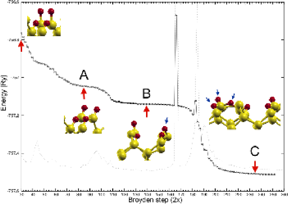
5.2 Electronic structure and the effect of oxidation
We present here the computed Kohn-Sham band structure of three models of oxidized Si(100). The electronic structure of the 1D and 1E’ surfaces is shown in Fig. 5.4 along a standard path in the surface brillouin zone: ---- (see Fig. 2.2 in chapter 2). Mostly, modifications respect to the clean Si(100)–c(42) concern a change of surface states inside the bandgap. In fact, comparing Fig. 4.18 to Fig. 5.4, it is evident that oxygens move the surface states visible in the - direction, states that are responsible of the S0 EEL peak of the clean surface, (see Fig. 4.13 and Fig. 4.12 in Chapter 4). The oxygen adsorbed modifies also bands in the - path.
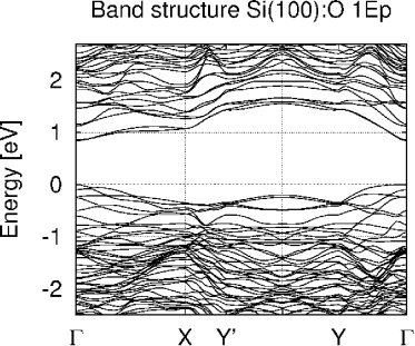 |
 |
Moreover, we present in Fig. 5.5 the computation of the electronic states for the surface including a silanone (O)Si=O bound. In Fig. 5.5 it is possible to see the flat bands in the ’- path due to the presence of oxygen doubly bonded to the top silicon of the dimer.

Furthermore we performed a test on the structure to better analyse the effect of the isolated Si=O bond. For this system we report the bands compared to that of the clean surface (see Fig. 5.6).

The bandgap typical of a semiconductor is closed by the presence
of oxygen, hence the system is metallic.
All calculations are performed within the DFT-LDA and
a scissor shift of eV (see sec. 4.5.5)
has been applied to the unoccupied bands in order to mimic the many body effects.
Band structure calculations are performed with the ABINIT package [122].
5.3 Experimental energy loss data
Experimental EEL spectra of the oxidized Si(100) surface
are not so numerous in litterature, at least in the range of energy
we are studying (i.e in general up to 8-10 eV and in particular up to 3 eV).
In this work we are refering to not-so-recent data from
Ibach et al. [116, 117] and at
the subsequent paper of Ludeke et al. [118]
where experimental REELS are reported in terms of the second derivative
of the spectrum respect to the energy in order to cut the large contribution
of the elastic peak and evidence spectral features.

In Fig. 5.7 all experimental data are collected.
The spectra from Ibach et al. are reported for the clean (black circles)
and oxidized (red circles) surface.
In particular, Ibach used high incident energy of the electrons,
(Ei=100 eV) and an off specular geometry with
normal incidence and collecting electrons at 42.5∘ respect
to the perpendicular direction to the surface plane.
From the analysis of Ibach’s data we can conclude that there are two features
that seems to be due to the oxygen adsorption:
a peak at around 7 eV, which appears in the oxidized surface, and the surface plasmon
at around 12 eV which is splitted in two.
Moreover, the bulk plasmon, appearing at 17 eV in the clean surface,
is lowered and slightly blueshifted.
The other experimental data reproduced in Figure 5.7
are from Ludeke et al. [118] (green, blue and violet
circles in Fig. 5.7) and refer to specular scattering geometry:
backscattered electrons are detected and analyzed. The three sets refers to
different incident energies: 24 eV (violet), 50 eV (blue) and 100 eV (green).
Peaks at 3 eV and 5 eV (E1 and E2 respectively)
appear in all those sets of data. From the comparison of the three sets
it is possible to conclude that the two main peaks around 5 eV and 7 eV are in
agreement with Ibach’s results.
Moreover the 7 eV peak increases with increasing incident electrons energy and
is interpreted by Ludeke et al. as an excitation of the SiO or SiO2
molecules [145, 146]
in the Schumann region.
We will comment this assignement in the following
paragraphs, where we will show that our results do not support it.
5.4 Theoretical energy loss spectra
In the following paragraphs we present REEL spectra calculations of the oxidized Si(100) surface using the code YAMBO [126].
5.4.1 Clean versus oxidized Si(100): the low-energy part of the spectrum
REEL spectra are often presented in literature in terms
of the second derivative of the energy loss. Moreover we start presenting
here our computed bare REEL spectra for the clean and oxidized Si(100).
In particular we considered the clean and the 0.5 ML oxygen-covered surfaces with
oxygen inserted into the bridge (1D) or the backbond (1E′).
We compare the REEL spectra computed for the experimental setup of
Farrell (Ref. [119]: specular scattering at
60∘ with incident energy Ei=40 eV) with measured spectra for the clean
Si(100).
All results are shown in Fig. 5.8 where theoretical spectra for
x and y polarization directions are also presented separately.
In the bottom panel of Fig. 5.8 a comparison of the
(unpolarized) experimental data with computed spectra averaged over the two
polarization directions is shown.

It is evident that the two main peaks, namely the S0 shoulder at 0.8 eV and the peak S1 at 1.3 eV in the experiments, appear also in the calculated spectra for both the clean (black line) and the oxidized 1E′ configurations (blue line). On the contrary, oxygen in the bridge position (1D structure- red line) completely kills the first peak of the spectrum. Unfortunatly we did not find experimental data for this surface at low oxygen coverage in the low energy range ( eV), but a similar behaviour is shown in the case of a coverage of H2O in Ref. [119]. In conclusion of this section we can say that REEL provide a useful tool able to distinghuish between oxidized surface configurations, in particular in the low energy spectral region.
5.4.2 Clean versus oxidized Si(100): REEL spectra in a wider spectral reagion
In this section we present computed REEL in terms of the second derivative spectrum. In Fig. 5.9 (top panel) we show the bare REEL spectra for the clean, the 1D and 1E′ structures (0.5 ML coverage) computed for the experimental setup used by Ibach and Ludeke in their works [116, 118] (i.e. incident energy Ei=100 eV with slightly different geometry scattering111Ibach used off specular experimental geometry instead of backscattering geometry form a normal incident beam of electrons used by Ludeke et al. in Ref. [118]. However, at this level of approximation we did not find appreciable differences in case of spectra calculated with specular or off specular geometry.). In the middle panel of Fig. 5.9 we show the computed second derivative spectrum. Neglecting oscillations for energies below 3 eV, and except for the intensity of the surface plasmon peak calculated around 15 eV, the clean and the other two oxidized surfaces do not show any important differences. This is in contrast with experiments (bottom panel of Fig. 5.9) where a peak centred at around 7 eV appears after oxidation. In order to understand the origin of this peak, we analysed the EEL spectra of all configurations presented in Section 5.1. Following arguments presented in Ref. [118] about the origin of the 7 eV peak, we show theoretical results for surfaces including a silanone bond on the and reconstructions of the clean Si(100) and an oxygen inserted in the dimer bridge (Fig. 5.10).

 |
 |
We found slight differences with respect to the previous calculations: the 7 eV peak still does not appear and the spectral features are similar for the clean and the oxidized surfaces. Unfortunatly, large differences between and structures appear in the low region of the spectrum where experimental data are not available. However we can observe that the surface plasmon is slightly lowered and blueshifted when a silanone bound is included in the surface configuration. Moreover we report in Fig. 5.10 (left) the results concerning the stable “C” structure and his metastable precursor “B” containing one (O)Si=O bound depicted in Fig. 5.3222 For silanone structures we used 72k points in the IBZ and 450 bands, corresponding to minimum – transition energy of 13.27 eV required 64k points and 500 bands, corresponding to 15.09 eV, for the “B” and “C” structures 72k points and 500 bands, corresponding to 15.09 eV, have been considered in order to fully converge..
Once more we can see that no features at 7 eV comparable to the experimental peak appears in our calculations, and even if Hemerick et al. [32] suggests similar structures on small clusters as energetically favorable, we can not conclude that silanone bond or siloxane structures on Si(100) are representative of the real surface. Moreover, Ludeke et al. guessed that the 7 eV peak was related to molecular excitations of Si=O bond or silicon monoxyde molecule. Calculations performed in the present work, however, rule out Si=O structures bonded to the surface.
It can be worth to mention that, taking as a reference
the surface plasmon peak of the clean Si(100) (represented
by the black continuous line in Figs. 5.9,
5.10), oxygen added
into 1D and 1E′ positions lowers the peak
(see Fig. 5.9), while oxygen added into
the silanone bonds lowers and redshifts the position
(see Fig. 5.10 left panel).
Conversely, calculated spectra for B or C configuration
show a shift of the peak position to the opposite direction
(see Fig. 5.10 right).
At this point, several speculations can be done in order to
explain the origin of the peak measured at 7.0 eV, which does
not appear in theoretical spectra for the considered structures.
From the point of view of calculations we must underline
that they are performed only at the RPA level.
A further analysis could call for the use of approximations
beyond RPA in order to describe eventually strong excitonic effects.
Moreovoer, we mention that the oxidation process of Si(100) is still under debate,
for example, we can not exclude the formation of
clusters of SiO2 during oxidation.
In addition, looking at the intensity dependence of the peak, increasing with the
energy of the incident electrons (see Fig. 5.7),
we could interpret the peak as due to
transitions from states originating from structures below the surface level,
in fact, higher energy electrons are expected to penetrate
deeper in the sample.
Within these hypotesis the present theory could not be adeguate to treat,
for example, multiscattering processes.
In addition we note that the experimental data are old and it is not clear
how well characterized and clean the surfaces are.
However we conclude that our calculations does not
support Ludeke’s interpretation about the origin of the 7 eV peak,
because does not appear in all the considered model surfaces
(including Si=O or O-Si-O bonds).
5.5 Conclusions
In the present section we draw a summary of the previous analysis,
and some conclusions.
We calculated the relaxed atomic position of several oxidized si(100)
surface reconstructions at 0.5ML (1D and 1E’) of coverage.
Moreover we analyzed 1ML coverage structures with a silanone bund
and an oxygen in the bridge of the dimer (1D Si=O), with a and a base.
Finally we found a structure “B” characterized by a silanone bond and
Si-O-Si-O-Si chains, to be the metastable precursore of the “C” structure,
the most stable, with one silicon atom bonded to three oxygens
(see Fig. 5.3).
We calculated the bare REEL spectrum in the cases
of the oxydized Si(100) previously considered.
We have been able to relate the change in the spectra with the changes in the
band structure in the case of both prototypical configuration (oxygen in the bridge
and oxygen in the backbond).
Furthermore we calculated the second derivative
spectra thanks to the implementation of the SG method in the YAMBO code [126].
This allowed us to compare EELS results with the experimental data.
We have shown that the excitation at 7 eV can not be related to
a molecular excitation of Si=O or O-Si-O, as suggested by Ludeke et al., because
the configuration with an oxygen on top of the higher silicon atom in the
dimer does not reproduce that structure.
At the moment we are not able to give an alternative explanation for the
origin of this spectral feature, but we can confirm that the reconstruction
studied in this paper (including the most stable structures 1D, 1E′,
1D Si=O and “C” and the metastable precursor with Si–O and SiO molecule)
do not reproduce this peak. Still, recent works by Hemerick et al. and Chabal et al. have pointed out the critic presence of silanone bonds during the oxidation
process.
We can only guess that including many body effects in the calculations could
provide more accurate theoretical results, taking into account self-energy and excitonic
effects, in order to help in shedding light on that problem.
Chapter 6 Subtleties in electronic excitations of open shell molecules
In this chapter we present a theoretical study of BeH, a simple heteronuclear diatomic molecule with an unpaired electron. We considered BeH molecule as the simplest exemple of an isolated open shell system for which the ground state is expected to be spin polarized. We present calculations of energy levels and density of states. Convergence studies and problems arising up in order to correctly describe excitation spectra are also underlined. At the end some excitation energies calculated for this system are compared to available experimental data and the agreement is discussed.
6.1 Brief review of TDDFT for isolated systems
In this section we briefly review the Casida’s approach to treat the molecular
excitation of isolated systems.
This framework is a reformulation of the TDDFT in the configuration space
and the details can be found in Ref. [147, 148].
In fact all the observables are represented using
the DFT–KS eigenvectors in such a way that the non–interacting
response function results to be diagonal.
We note that in case of isolated systems the physical
quantity we deal with is the polarizability of the system
that is defined when an external perturbation
is applied to the system.
In this case the x component of the dipole momentum is defined by:
where q is the charge of the electron and
.
Hence, the polarizability is defined by:
| (6.1) |
and using the Lehmann representation it can be written by:
| (6.2) |
Where are the energies and the many body wavefunctions of the excited and ground state respectively. Using the basis set of operators we can define the quantity:
| (6.3) |
corresponding to the density in the configuration space, for which the following relations held:
| (6.4) | |||
| (6.5) |
where the KS response function is written over this basis set:
| (6.6) | |||||
In case of independent particles and applying the and operators we obtain the reduced expression for the response function:
| (6.7) |
Hence, in the configuration space the TDDFT equation held the form (see Ref. [147, 148]):
| (6.8) |
This equation can be reorganized and written as a matrix equation (see Ref. [147, 148] for mathematical details) exploiting the hermitian nature of the kernel . Moreover assuming that the KS orbitals and the kernel are real quantities (infinite lifetime of the excitations) and after some algebra we can write:
where:
| (6.9) | |||||
| (6.10) | |||||
| (6.11) |
and the polarizability as:
| (6.12) |
where and . Finally, comparing this last expression (6.12) with eq. (6.2) it is possible to write the eigenvalue equation:
| (6.13) |
where:
Eq. (6.13) is called Casida equation (see Ref. [147, 148]) and allows to map the problem of finding the excitation spectrum of a system too an eigenvalue problem for the matrix .
6.2 Closed and open shell systems: the problem of the correct counting of excitations
We divide now the discussion to the case of closed and open shell systems. In the first case the approach presented in the previous section predicts, in principle, the correct excitation energies. However, in the second case some problem limits its straightforward applicability. In the next paragraphs we present the problem with an example.
6.2.1 Closed shell systems
Let us start with the case of the closed shell systems, i.e. systems having the same wavefunction for the two spin channels. In this case it is possible to diagonalize the matrix, presented in the previous section, exploiting the symmetries resulting from the adiabatic approximation.

Let us consider a three levels system consisting of two electrons (see Fig. 6.1), the ground state is characterized by two coupled electrons both occuping the level, two additional unoccupied levels and are available to the excitations. A spin–unpolarized ground state is expected and the matrix has important symmetry properties, so that its eigenvectors will be either symmetric or anti-symmetric with rispect to spin flip. Assuming the adiabatic approximation, the matrix, can be written as:
such that :
The eq. (6.13) is decoupled in:
| (6.15) | |||
| (6.16) |
In case of eq. (6.15) for a given electron–hole pair, both spin channels interfere constructively, TD total charge changes, but not the TD magnetization (Spin-singlet excited state). Conversely in case of eq. (6.16) both spin channels interfere destructively, no TD total charge change, TD magnetization change (Spin-triplet excited state). In this case the resulting eigenvectors are written in the form:
Hence, summarizing, it is possible to group the results in two kind of excitations:
| (6.17) |
and
| (6.18) | |||||
| (6.19) | |||||
| (6.20) |
This states are simultaneous eigenvectors of H, S2 and Sz.
6.2.2 The problem of the open shell systems
The simplest case of a system with spin–polarized ground state consists of three electrons that can be arranged within three levels. Fig. (6.2) describe the ground state configuration and the possible spin–collinear excitations.

In this case the matrix does not have the same symmetries
presented in the previous section. This time it contains the
elements related to the excitations , , and
resulting with dimension. Moreover any symmetry does not
allow to divide by blocks the whole . However the selection rules
allow to group the excitations in two sets: conserving the spin and
those for which .
Diagonalizing H, S2 and Sz simultaneously we
obtain the following doublet for the ground state:
and the excited states (doublet):
| (6.21) | |||||
| (6.22) | |||||
| (6.23) | |||||
| (6.24) |
and the quadruplet:
| (6.25) |
where we adopted the notation to indicate the spin occupation of the state.
The double excitation , represented by the yellow square in fig. 6.2,
is present because the eigenvectors
must be simultaneous solutions of the eigenvalue problem for H and S2.
The excitations of this system present states with three half occupied levels
(see Fig. 6.2) that are mixed by the S2 operator
with similar states with inverted spins.
It is worth to note that this kind of excitations are missing when
we attempt to build the eigenstates of H, S2 and Sz
starting from the single particle excitations. In this case we obtain three doublet:
| (6.26) | |||||
| (6.27) | |||||
| (6.28) |
and a triplet:
| (6.29) |
As the theory is exact and the sole quantity requiring an approximation is the kernel
the lack of the excitations description is due to the adiabatic assumption.
The research of an improved kernel able to correctly describe the missed excitations is
beyond the scope of this thesis.
However, in the following paragraphs an application to the case of the
calculations of the excitation energies of the
BeH molecule is presented.
6.3 A simple open shell molecule: BeH
A BeH molecule consists of five electrons, four due to
Beryllium and one to Hydrogen.
Configuration of the Beryllium atom (4Be: ) suggests
his divalent nature, in fact usually the two electrons in the level
are not involved in chemical bonds.
Therefore we describe the joint effect of the core and the
inner electrons of Beryllium with a suitable pseudopotential.
In particular we used a Troullier–Martins LDA pseudopotential
available in the on line repository of the ABINIT code [68, 122].
Following this recipe, only three valence electrons
of the molecule are involved in DFT calculations and are expected to determine the
main properties of BeH, including the spin polarization of its ground state.
Bond length between Beryllium and Hydrogen is assumed to
be RÅ (see Ref. [149])
and the cubic supercell is centred in the middle point of
the line joining the centers of the two atoms.
A schematic representation of the molecule is depicted in
Figure 6.3 where the active electrons (blue and red circles)
are underlined and distinguished respect to the spectator electrons
(white circles).
Spin variable is also shown in order to evidence that spin
is not compensated.

In the following paragraphs we will show our results about spin resolved calculations performed with the ABINIT package [68].
6.4 Energy levels and density of states
In order to obtain converged energy levels and
the spin resolved density of states of BeH, we
performed total energy minimization within
DFT in local spin density approximation.
We obtained the theoretical energy levels
(see Fig. 6.4) imposing a convergence
tolerance of Ha2 for the largest squared residual defined by:
.
In order to establish reliable results we performed
convergence tests on the supercell size
(see Sec. 6.4.1).
Here we comment the results summarized in Table 6.1.
We compared our results with theoretical calculations
reported in Ref. [149] and
experiments from Ref. [150].
We obtained a satisfactory agreement of the
Kohn and Sham energy of the highest occupied orbital
with respect to calculations performed in Ref. [149]
with localized basis orbital.

Even if there is not analogous of the Koopmans theorem, providing a physical
interpretation of the Hartree Fock eigenenergies, for the KS
eigenvalues, it is possible to interpret the highest occupied molecular orbital (HOMO)
energy calculated within DFT as the ionization energy of the system
(see ref. [151]).
However in the present case of the BeH molecule, if we assume that the E
energy referred to the vacuum should be the ionization energy of the system,
we face with a discrepancy with respect to the experimental value reported in Ref. [150].
In fact, the experimental value of 8.21 eV disagrees with
eV, calculated within DFT-LSDA,
and also with 4.60 eV obtained in Ref. [149].

This discrepancy is due to the inadequacy of the
LDA exchange and correlation potential
(see Ref. [152, 153])
that does not have an asymptotic required behaviour.
This fact lead to the lack in the description of the levels staying close
to the vacuum region and the excitation energies
of the molecule involving these levels.
Figure 6.5 represents the distribution of
the density of states obtained after convergence tests,
discussed in detail in Sec. 6.4.1 and,
in Figure 6.5, we report the
density of states (DOS) calculated within the same approximations.
When spin symmetry is broken, BeH molecule shows an
asymmetric distribution of DOS (see Fig. 6.5)
with respect to the two spin channels.
We considered a cutoff energy E Ha and a cell size
a Ha as converged values.
The first three peaks, centred at eV, eV and eV
represent the occupied states, also depicted in
Fig. 6.4, moreover
and orbitals are shown, in particular
the height of peaks related to orbitals is doubled
with respect to the orbitals bacause of their
degenerancy giving contributions to the DOS peak coming
from a double number of states.
A smearing of 0.008 Ha is applied to both distributions.
6.4.1 Convergence issues
Convergence tests have been performed respect to two quantities: (i) the cutoff energy determining the number of plane wave of the basis set and (ii) the supercell dimension .
In order to determine a suitable value for we checked the values of the KS-eigenvalues: E, E and E, corresponding to the occupied states (see Figure 6.4 and Table 6.1). Since we used a Troullier–Martin (TM) pseudopotential for Be, we found a resonable converged value of EHa (corresponding to 36Ry) see Table 6.1 and Fig. 6.4. However we verified that E Ha can be considered a converged value in order to calculate the first excited states of the molecule, in fact, the HOMO–LUMO distance for each spin channel does not change significantly. Table 6.1 summarize the converged values for and , that distances are also evidenced in Fig. 6.4.

Moreover, a set of tests with respect to the cell size have been performed
in order to find the best compromise between accuracy and
practical feasibility of calculations.
In fact, a large vacuum region around the molecule is required
in order to obtain the correct behaviour of continuum states above
the vacuum level (see Fig. 6.7)
and to avoid spurious interactions between replicas,
however this request can increase significantly the
computational workload.
It is worth to mention that a good choice of the cell shape
(see Fig. 6.6) can slightly optimize the
numerical convergence.
We considered the molecule placed in the middle of a cube
of length () with the straight line joining
Beryllium and Hydrogen atoms parallel to
one face of the cube (Fig. 6.6(b)).
We performed several tests increasing for a fixed cutoff energy and number of bands. In Fig. 6.7 a summary of the results is depicted: in the actual range of considered, occupied states slightly change because of the dimension of the supercell, on the contrary the unoccupied levels are strongly influenced and require a large cell size ( Bohr). This fact can be important if we want to calcuate excited energies involving higher energy levels. In Fig. 6.4 we can distinguish discrete unoccupied states () and a thick serie of states above the vacuum level (grey region). In fact, increasing the cell size, the upper levels become closer and closer with each other (see Fig. 6.7) and a continuum of states, in the limit case of an infinite supercell.
| Level | present work | Ref. [154] | Ref. [149] | Exp. Ref. [150] |
|---|---|---|---|---|
| -8.35 | -8.35 | - | - | |
| -8.01 | -7.99 | - | - | |
| -4.62 | -4.63 | -4.60 | 8.21 | |
| HOMO–LUMO | present work | Ref [154] | ||
| 2.28 | 2.29 | |||
| 5.07 | 5.16 |

In conclusion we assumed that a cell size of 55 Bohr is required in order to correctly calculate the three lowest eigenvalues. On the contrary, for excited states calculations, involving higher energy levels in the vacuum, a larger cell is recommended. Our conclusions are in agreement with a slightly different treatment discussed in Ref. [154].
6.5 Excitation energies
In this section we report results concerning excited state calculations within the TDLSDA formalism. For that we used a recent implementation of the method in the ABINIT software [68, 122, 154]. In Table 6.2 we summarize the results about the main excitation energies calculated. We did not consider excitations involving continuum states because they are extremely influenced by the countour conditions. However, in order to have more reliable results we used a larger supercell with respect to the case of ground state calculations, in particular a 707070 Bohr cubic cell is considered with a cutoff energy of 10 Ha and 50 bands.
Even if the ionization energy disagrees with respect to experimental data making a shorter distance between occupied states and vacuum level, our first calculated excitation energy connecting the spin-collinear states is comparable with experimental value reported in Ref. [155]. The TDLSDA theoretical value ( eV) understimates the experimental measure ( eV) but improves the DFT-LSDA HOMO-LUMO distance ( eV) calculated as a bare difference between Kohn-Sham eigenvalues (see Table 6.1 and 6.2).
However we observed that every excitation involving states higher than the level are strongly influence by the cell size. For this reason we evidenced with bold carachter in Table 6.2 the more reliable results, i.e. excitations excluding states above .
| Excitation | elec. conf. | this work | Ref. [149] | Ref. [156] | Exp.a | Exp.b |
|---|---|---|---|---|---|---|
| 2.37 | 2.391 | 2.2479 | 2.56 | 2.48 | ||
| 4.51 | 4.593 | 4.5103 | 5.51 | - | ||
| 4.62 | - | 4.6300 | 5.61 | - | ||
| 4.70 | - | 4.7047 | 6.31 | 6.317 | ||
| 5.41 | 5.129 | 4.8049 | - | - | ||
| 5.66 | - | 5.1685 | - | - | ||
| 7.15 | - | - | - | 7.46 | ||
| 8.01 | - | - | - | - |
Moreover we underline that the excitations,
involving three half occupied states
(),
appear at two excitation energies (5.66 eV and 7.15 eV)
and with the same orbital configuration.
These -excitations are distinguished by their total spin, i.e.
S in one case and higer total spin in the other.
Thanks to the Hund’s rule we can identify the excitation with S with
higer energy ( eV), and this lead us to discard the 5.66 eV
excitation.
A different argument leads Casida et al. to reject the same
excitation identifying the same excitation we discarded as
spin contaminated.
Comparison with experiments available in
Ref. [155, 157]
are satisfactory, in particular with respect to the
case of
and
excitations.
Discrepancy about excitation
is due to the problem previously underlined: in fact states are higer
than level.
Comparison with results obtained in Ref. [149, 156]
are also aligned with our conclusions.
6.6 Conclusions
We studied the BeH molecule as the simplest exemple of open shell system. In our pseudopotential approach only three valence electrons are involved in the eigenvalue problem, for this reason total spin is not compensate and the electronic ground state is spin polarized.
Spin resolved density of states and energy levels have been computed within DFT–LDA approach. Convergence tests with respect to the supercell size have shown the sensitivity of the unoccupied states above the vacuum level to the cell dimension. Moreover we found a discrepancy between the energy of the HOMO orbital calcualted (in agreement with others theoretical works, see ref. [149] and [156]) and the ionization energy measured. This is due to the well known inadequacy of the asimptotic behaviour of the LDA exchange and correlations potential.
In conclusion we calculated the first excitation energies of the molecule using TDDFT within the adiabatic approximation. We compared our reliable results with experimental data finding a satisfactory agreement even if a part of the excitations can not be reproduced by frequency–independent kernels such as the ALDA one.
Chapter 7 A paradigmatic case for semicore and spin-polarization effects
in electronic spectra of solids:
bulk iron
Semicore states of transition metals such as iron are outside the reach of “standard” pseudopotential of DFT which, even when non linear core corrections are adopted, include them in the frozen atomic core. In this work we present an analysis of several pseudopotentials for iron generated in the Troullier Martins and Hamann scheme assuming both local density and generalized gradient approximations (LDA, GGA) for the exchange–correlation functional and considering core-valence partitions with and without including semicore orbitals among valence states. Non linear core corrections are considered and the pseudopotential transferability has been checked. We calculate structural and electronic properties of the phase of iron and we present a comparison between calculated optical conductivity and experimental data.
7.1 Pseudopotentials for iron
Pseudopotentials (PP) are a well-established tool in ab initio structure calculations of solids. A review of the topic can be found in literature ranging from the most influential works [10, 11, 12, 13, 14, 15, 16, 17] to other important but less fundamental papers [18, 19, 20, 21]. Important advantages of the pseudopotential approach can be summarized in the following two points: first, by replacing the atom by a pseudoatom, the number of orbitals which have to be calculated is reduced, and, second, using plane waves, the size of the basis set can be substantially reduced, because the pseudo-wavefunctions are smoother than their all-electron counterparts.
However in all cases where an overlap between valence and core wave functions
exists, the frozen core approximation underlying the construction of
all pseudopotentials is not well satisfied.
One way to overcome this problem is the inclusion of a core correction considering
the non linear contribution of the core charge to the
exchange-correlation potential (NLCC).
Another more straightforward solution is
the explicit inclusion of the semicore electrons into the valence shell.
In this work we considered both these approaches in order to build
pseudopotentials for the specific case of iron.
Such pseudopotentials are used to calculate the structural and electronic
properties of the phase of bulk iron. In conclusion we report our results
for the optical conductivity compared with experimental data.
The wavefunctions of iron are strongly localized and show a significant overlap with
the orbitals, although the latter are much lower
in energy.
Looking at Fig. 7.1, it is evident that
the separation of the electronic system into well-isolated core and
valence shells is ambiguous, because of the large overlap between
and states.
For this reason, we considered two electronic configurations:
one with 8 ( states) and the other with 16 ( states) valence electrons.
We used two schemes for pseudopotential generation, referring to
Hamann [21] and
Troullier–Martins [20] works respectively.
In the former scheme a fixed cutoff radius rcl by an exponential function
, in the latter scheme wavefunctions
are built with a parametric form
below rcl, where is a polynomial of order six in r2.
In the case of a standard pseudoatom with 8 valence electrons we verified
the importance of including non linear core corrections (NLCC) to correct
GGA pseudopotentials presenting fake wiggles in the r 0 limit due to the
gradient dependence of the exchange-correlation approximation.
In the case of a 16 electrons pseudoatom we could
not generate a transferable pseudopotential in
generalized gradient approximation, neither in
the Troullier-Martins nor in the Hamann scheme.
The only pseudopotential with good transferability was
generated within the local density approximation following
the Hamann scheme.

 |
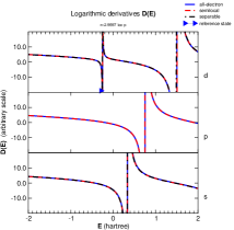 |
In order to check the pseudopotential transferability
we studied logarithmic derivatives and compared them to the
their all-electrons counterpart.
Figure 7.2 shows logarithmic derivatives in case
of Troullier–Martins (left) and Hamann (right) pseudopotentials
respectively.
Hamann pseudopotential are clearly more transferable, and therefore
more accurate in describing scattering properties.
However we should be aware that Hamann pseudopotentials are
usually much more expensive in terms of plane waves required for convergence
than the ones generated within the Troullier Martins scheme.
As a general rule, depending on the specific system and properties we want to describe, a compromise between accuracy and efficiency should guide the choice of the suitable pseudopotential.
7.2 Properties of bulk iron
In this section we report the results of DFT calculations of structural and electronic properties of bulk iron. We also show a Time Dependent DFT calculation of the optical conductivity, and we compare our results with experimental data.
7.2.1 Structural properties
An useful comparison between the generated PP can be based on the evaluation of physical quantities. In particular we calculated the lattice parameter of iron. We considered iron in his phase, the most stable at normal temperatures, where the metal presents a body centred cubic (BCC) crystal structure.
The optimized value of has been obtained by an estimation of the minimum of the Birch–Murnaghan [158, 159] equation of state for solids:
| (7.1) |
where is the bulk modulus and is the cell volume at the minimum. We used the ABINIT package [68, 122] to compute converged total energy for different values of the cell parameter a0, and we fitted the obtainted points with Eq. 7.1 (see Fig. 7.3).

| Pseudopotential | a0 | B0 | |
|---|---|---|---|
| [Bohr] | [GPa] | ||
| 8e- TM GGA NLCC | 5.56 | 67.86 | 2.47 |
| 8e- TM LDA NLCC | 5.34 | 106.31 | 2.11 |
| 16e- H LDA NLCC | 5.27 | 101.23 | 2.19 |
| Exp.(a) | 5.42 | 168 | 2.22 |
7.3 Electronic properties
7.3.1 Electronic properties
We present here our results for the density of states (DOS) around the Fermi energy and the electronic band structure including semicore states. These calculations have been performed with the ABINIT package [68] in local spin density approximation (LSDA). We verified that a random sampling of k points in the Brillouin Zone (BZ) is more efficient than the use of a regular grid, in fact with 5000 k DOS is converged. In Fig. 7.4 two curves represent converged DOS where the two spin channels show an asymmetric distribution allowing to identify the majority and minority component.
 |
The corresponding band structure is presented in Fig. 7.5,
where high symmetry crystallographic directions are chosen
in agreement with previous
literature [162, 163, 164].
We used Hamann LDA pseudopotentials generated including semicore
states in order to describe the core bands and bands.
We obtain band energies of Fe-3s (85 eV) and Fe-3p (52 eV)
as depicted in Fig. 7.5.
In the same figure we show the effect of the spin on the electronic
properties, removing most of the accidental degenerancies
of band structure and splitting the flat core states.
In addition we report in Fig. 7.6 (top panel) a comparison
between bands calculated within LDA or GGA, concluding that
the GGA corrections do not change dramatically the electronic
structure making LDA a satisfactory approximation for our scope.
Even the use of semicore PP (bottom panel in Fig. 7.6)
do not influence considerably the estimation of valence states,
therefore it is possible to conclude that our approximations
are reasonable in order to predict correctly the optical properties
of bulk iron.
On the contrary, the case of levels is more subtle.
In fact, because the angular momentum is not zero
for levels (i.e. =1), the total quantum number
must be considered, and the spin orbit
coupling can influence the exact degenerancy and position of the bands.
Even if this case will not be treated in the present work, because
beyond the aim of the thesis, it is worth to mention that a fully
relativistic approach is required in order to obtain reliable
results for this kind of states.
Conversely, the states are correctly predicted within
the DFT–LSDA approach and the up–down splitting
is comparable with the available experimental
data [161].
For completeness, we report in Tab. 7.2
the calculated splitting and dispersion of both the and
levels.
| state | Dispersion | ||
|---|---|---|---|
| [eV] | [meV] | [eV] | |
| 3.03 | 360 (at N) | - | |
| 3.15 | 120 (at ) | 4.9 |

 |
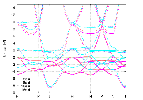 |
In conclusion we also report an analysis of the
relation between total magnetization of iron and
the 3 splitting.
It was suggested in the past [165, 166]
that core-level splitting could
be used to monitor the magnetic moment or the hyperfine field,
because the splitting should vary linearly with the spin
state of the unfilled inner shell.
X-ray photoelectron spectroscopy (XPS) measurements for nonmetallic
transition metal compounds, on rare-earth metals
and ionic compounds [165, 166, 167]
are compatible with this scheme.
However, Fe-3 XPS splitting studied in crystalline and amorphous alloys
have shown a poor correlation between the 3 splitting
and the magnetic moment of the solid
(see Fig. 3 in Ref. [161]).
Our calculations show a linear relation of such a splitting
with respect to the total magnetization of bulk iron
(see Fig. 7.7 top panel), giving some
basis to better investigate the apparent disagreement
with experimental data.
We calculated the total magnetization defined as the
difference between the majority and minority spin density
integrated over the unit cell .
This quantities has been evaluated for several lattice
parameter values of bulk Fe, centred around the
experimental one (5.42 Bohr).
Changes of the lattice parameter influence
the local distance between atoms, reproducing the effect of
a change of pressure. Moreover changes on lattice geometry affect
total magnetization.
The dependence of the splitting with respect to the
pressure is shown in Fig. 7.7 bottom panel.
 |
 |
7.4 Optical conductivity
In this last section we report the calculations of the dielectric function () obtained within the indipendent particle random phase approximation (IP-RPA) and including crystal local fields effects (RPA-LF). This quantity is closely related to the electronic structure and follows straightforward from theory, however experiments are often presented in terms of the optical conductivity (, see Refs. [168]). However, and are connected by the well known relations:
| (7.2) | |||||
| (7.3) |
In Fig. 7.8 we show the optical conductivity of bulk iron
calculated with the DP code [78].
There is a nice agreement between the calculated curves
and the experimental data reported in Ref. [168]
with respect to the general shape and the position of the maxima.
We have not included any intraband contribution in our calculation and
this is the reason why the sharp structure in the low–energy region
of the experimental spectra is not reproduced (Fig. 7.8).
We report, for comparison, a recent calculation of the
optical conductivity including the Drude peak
(see Ref. [169]
for details about the treatment of the intraband transitions), in
order to show that only the low energy part of the spectum
is affected by this approximation.
Spin flip is also not allowed and this bring us to conclude that
the maximum of the computed conductivity near 2.5 eV results
from transitions between collinear spin states, in particular
between states of the majority spin channel.
It is easy to identify these excitations looking at Fig. 7.4:
transitions connect occupied states and the unoccupied
states just above the Fermi energy for the same spin channel (dashed line).
Crystal local fields have negligible effects, and this is
in agreement with the cases of others metals.
As shown in Fig. 7.8 by the red and blue lines.

7.5 Conclusions
We succeeded in generating a set of pseudopotentials for iron, a prototypical transition metal for which an obvious separation between core and valence orbitals does not exist.
Semicore states have been either explicitly included in the valence set, or treated within the usual non linear core corrections scheme. Our set of PP has been tested against structural and electronic properties of BCC bulk iron, including the lattice constant, spin resolved density of states, band structure.
We also reported an analysis of the Fe-3s splitting with respect to the total magnetization. We found a linear dependence between these two quantities and between splitting and the lattice parameter. This results support the use of the s core-level splitting as a monitor of magnetization, and are compatible with a similar behaviour presented by non metallic transition metal compounds, rare earth metals and ionic compounds. Moreover we found that the 3s splitting calculated at the experimental value of the lattice parameter substantially agrees with XPS core level measurements reported in Ref. [161]. However the linear trend theoretically predicted is in apparent disagreement with experimental results where 3s XPS peak splittings do not correlate with the Fe magnetic moments.
Concerning the optical conductivity good agreement between RPA results and the experimental data is found. This allows one to conclude that the main spectral feature are well reproduecd by spin-collinear excitations.
Chapter 8 Iron, cobalt and nickel pyrites
Transition-metal pyrites form a series of compounds with a large variety
in electrical, magnetic and optical properties.
In particular, recently there has been a renewed interest in
iron, cobalt and nickel disulfides because of their potential
in future technological applications.
Iron and nickel-controlled doping of CoS2 gives rise to a tunable
source of highly spin-polarized electrons [170].
This property is extremely interesting to design new devices exploiting
the spin character of the electrons in addition to their charge.
In fact the essence of the current focus area termed spintronic,
or spin-electronics, is to use the electron’s spin, as well
as its charge in creating new devices or enhancing the functionality
of the existing ones [171, 172].
In this section we will present structural, magnetic
and electronic properties of FeS2, CoS2 and NiS2
calculated within the density functional theory framework. A
comparison of our results with respect to experimental data and to previous
calculations is also discussed.
8.1 Motivations
The rapid developement of spin valve-based magnetic read heads
and the emergence of spintronic [171, 172]
has thrown up a need for a better understanding of
spin-polarized materials [173].
Spintronic is based on the up or down spin of the carriers
rather than on electrons or holes as in traditional semiconductors
electronics.
In particular spin-polarized transport will occur naturally in any
material for which there is an imbalance of the spin populations
at the Fermi level.
This imbalance is present in ferromagnetic metals where the
density of states for spin up and down electrons are
shifted in energy with respect to each other.
Commonly in these materials there is an unequal filling of the bands,
which is the source of the net magnetic moment,
and causing the up and down carriers at the Fermi level to be
different in number, character, and mobility.
This inequality produces a net spin polarization
but the sign and magnitude of that polarization depends on
the specific material.
Materials having at the Fermi level only one occupied spin band
are usually called half metals (see Fig. 8.1).
A fundamental component in any spintronic device is a ferromagnetic
electrode which is used as a source of polarized electrons, and
an high value of spin polarization
P=(N↑-N↓)/(N↑+N↓) at the Fermi level
can provide significant benefits.
When the spin polarized electron current crosses
a sample having a non zero total magnetization
the only states that are available to the carriers are those
for which the spins of the carriers are parallel to the spin
direction of those states at the Fermi level.

If the magnetization of the material is reversed,
the spin direction of those states also reverses.
Thus, depending on the direction of magnetization of
a material relative to the spin polarization of the current,
a material can be either a conductor or an insulator for electrons of a
specific spin polarization (see Fig. 8.2).
The largest effect is generally seen for the
most highly polarized currents, therefore, there are continuing
efforts to find 100% spin-polarized conducting materials.
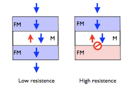
However, partially polarized materials
(such as Fe, Co, Ni and their alloys), are adequate
to develop technologically useful devices and can show
unexpected properties.
For example, transition metal compounds have beed attracting
extensive attention for that reason. Among them, FeS2, CoS2 and NiS2
have been studied from the
experimental [174, 175, 176, 177]
and theoretical [178, 179, 180]
point of view.
Moreover these compounds have been used to build and to
study Co1-xFexS2 and Ni1-xCoxS2 compounds,
recently predicted to be tunable half metals (see
Refs. [181, 177, 182, 183, 184]
for a review of works on Co1-xFexS2 and
Ref. [185] for Ni1-xCoxS2).
In the following sections we will focus on structural and magnetic
properties of FeS2 and CoS2, as a first step to be able in the
future to describe more complex compounds.
8.2 Structural and magnetic properties
All transition metal disulfides (MS2 with M a 3–transition metal atom),
crystallize in a cubic pyrite structure of space group
in which metal atoms are located
in face-centred postions. Structure can be
considered as an NaCl-like grouping of metal and chalcogen
atom pairs (sulfurs).
In Fig. 8.3 the atoms arrangement is shown from three
perpendicular views. Every metal atoms (dark grey circles) is surrounded
by six nearest-neighbour sulfurs in a distorted octahedral environment,
while each sulfur (light grey circles) bonds to one sulfur
(S-S bond) and three metals in a distorted tetrahedral arrangement.
Distance of sulfur–sulfur pairs (S–S) is short because of a
covalent bond.
The formation of S–S pairs is characteristic feature of
these structures.
In particular metal atoms are located at the positions
(0,0,0), (0,1/2,1/2), (1/2,0,1/2) and (1/2,1/2,0),
the eight sulfur atoms instead
are located at position
, ,
, .
The values of and (the lattice parameter)
are taken from Wyckoff [186], in particular we used
and Å in case of FeS2,
and Å in case of CoS2 and
and Å in case of NiS2.

We performed a geometric optimization using the BFGS algorithm [141, 142, 143, 144] with the ABINIT [68] code. The optimized S–S distances of FeS2, CoS2 and NiS2 are reported in Tab. 8.1, and compared with values reported in Ref. [178]. All the ground state calculations have been performed within the DFT-GGA framework (Perdew-Burke-Ernzerhof (PBE) parametrization [9]) with a cutoff energy E Ha. The geometry relaxation is performed by setting a tolerance of on the ratio of differences of forces to maximum force, reached twice successively, will cause a self consistent cycle to stop.
| System | [Å] | S–S [Å] | S–S [Å] | /at. [] | /at. [] |
|---|---|---|---|---|---|
| Ref. [186] | this work | from Ref. [178] | this work | Ref. [174, 181] | |
| FeS2 | 5.407 | 2.18 | 2.14 | ||
| CoS2 | 5.524 | 2.29 | 2.12 | 0.98 | 0.9 |
| NiS2 | 5.677 | 2.06 | 2.06 | 0 | - |
The agreement of the computed S–S distance with respect to
previous calculations is reasonable, as listed in Tab. 8.1.
Moreover, Figure 8.4 shows the electronic density distribution
for a suitable value of the chosen isosurfaces in order to evidence
the formation of the characteristic S–S bond
in the center of the crystal structure.
The magnetic character of the electronic ground state
of all the compounds has been also analyzed.
The values of total magnetization per metal atom are reported in Tab. 8.1
with experimental reference values reproduced from literature.
The three compounds display different behaviours:
FeS2 presents a total magnetization close to zero,
CoS2 has a ferromagnetic ground state with
total magnetization per cobalt atom close to 1 ,
and NiS2 is non–magnetic.
Experimental studies on transition metal disulfides
(see Ref. [174]) revealed the non magnetic
nature of all this class of compounds, except for the case of CoS2.
Experiments indicate that FeS2 as well as NiS2 are
paramagnetic semiconductors. In addition, at low temperature
NiS2 presents a transition to an antiferromagnetic phase.
Our calculations predict correctly this behaviour.
In particular for CoS2 we find a ground state electronic configuration
with a total magnetic moment 0.98 per
cobalt atom at T=0∘ K, which is close to the experimental value
0.9 (see Ref. [174]).
In addition we report in Fig. 8.5
the electronic density isosurfaces that evidences
the distribution of spin up and spin down components.
In the case of FeS2 the spin up and down
charge distributions are located at the same positions without any
motif distinguishig between the two components.
On the contrary, in case of CoS2 it is possible to appreciate a regular
ordering of the electronic density distribution according to the two spin
components (red and blue respectively in Fig. 8.5).
The maxima of the distributions are located at the metal sites of the
crystal and the up-down spin density is alternated in adiacent sites.
NiS2 still presents a regular ordering of the spin
density distributions but, as the total magnetization is found to be
zero, suggests an antiferromagnetic character.
Even if the study of NiS2 is beyond the scope of this thesis, we notice
that this result is in agreement with Ref. [174].

8.3 Electronic properties
In order to analyze the electronic properties of FeS2, CoS2 and NiS2
we calculated the spin resolved density of state (DOS) within DFT-GGA (PBE parametrization).
The software ABINIT [68] has been used in order to perform convergence
study and calculate the final distribution.
For FeS2 we used a Monkorst Pack [83] grid of
k points in the Brillouin zone (BZ), corresponding to 76 k, applying
a rigid shift of in the three spatial directions.
For CoS2 the grid consisted of k
points and for NiS2.
A thermal broadening (cold smearing) Ha is applied to simulate
the metallic occupation of levels following the recipe of
Ref. [187]111The smeared delta function is
defined by:
where , this choice minimizes the bump..
Density of states are calculated using the tetrahedron method giving a faster
convergence over the number of k poins required with respect
to the standard integration over the Brillouin zone.
In Fig. 8.6 the DOS of FeS2, CoS2 and NiS2
are shown. The three compounds present a similar density of states
but different electronic behaviour.
We discuss now our results that are in general agreement
with experimental
works [175, 176, 188]
and theoretical calculations based on linear combination of atomic orbital
(LCAO) or semiempirical and self-consistent tight-binding (TB)
approach [178, 179, 189].
The first two lowest energy bands are associated with bonding and
antibonding pairs of orbitals of the sulfur atom dimers
(s and s orbitals).
The following complex structure is due to sulfur 3 and
the metal 3 orbitals.
Then the crystal field of the disulfide anions (sulfurs)
splits the cation (metal) 3 non–bonding
orbitals into three low-lying 3 and two
higher-energy 3 levels (see Fig. 8.6).
All the disulfides studied have completely filled
3 orbitals, and as the atomic number increases
the additional electrons (none for iron, one for cobalt
and two for nickel) fill in the 3 orbitals.
The different filling of these bands determine the
electronic nature of the three compounds studied.
In particular, our calculations predict FeS2 as
a small band gap semiconductor, in agreement with
experiments (optical and conductivity
measurements [176] and X–ray
photoemission spectoscopy [175, 190])
and theoretical works [178, 179].
From our calculations the value of the FeS2 band gap turns out
to be 1.2 eV and 0.98 eV for the spin-up and spin-down components respectively
(Fig. 8.6, top panel).
Even if a more detailed analysis including
band structure calculations is required,
we can already conclude that the calculated values
are close to the experimental ones ranging from
0.9 eV to 1.2 eV (see Ref. [176])
and for which there is no general consensus.
Difficulties in the exact experimental determination of the band gap
of FeS2 could rise because of a large difference between
the indirect and direct gap as pointed out by
Zhao et al. [179].
In fact in that work all calculations in the local
density approximation lead to a minimum indirect gap
E eV and to a smallest direct gap E eV.
Concerning CoS2, we found similar structures
for low-energy states with respect to FeS2, but shifted
to lower energies (see Fig. 8.6, central panel).
Moreover our DFT-GGA calculations confirm the half metallic nature
of CoS2, where the two spin components present
density of states characteristic of a semiconductor (red line)
or a metal (blue line).
In Fig. 8.6 the Fermi energy
is set to zero for clarity.
It is worth to mention that half–metallicity of CoS2
has been recently discussed in literature from both the
experimental and theoretical points of view.
Direct measurements of spin polarization and
magnetotransport [170]
show that CoS2 is not completely polarized
(i.e.
is not large).
On the contrary, the temperature variation of the electronic
structure, studied by means of optical reflectivity measurements confirms
the half metallicity of the compound.
From the theoretical point of view
Shishidou et al. [180]
presented a detailed comparison between LDA and GGA
electronic structure calculations within
density functional, full potential linearized augmented
plane waves calculations.
In that work the authors conclude that GGA greatly
modifies the LDA band structure
from metallic to half metallic.
These conclusions are in agreement with our finding
displayed in Fig. 8.6.

In the case of NiS2 the spin density of states presents a symmetric behaviour that confirm the apparently non magnetic nature of that compound and the zero total magnetization obtained from our calculations (see sec. 8.2). However, as underlined preivously, NiS2 presents a local regular ordering of the spin density distribution justifying its antiferromagnetic nature (see Refs. [191]). Among the transition metal disulfides, NiS2 is considered to be a Mott-Hubbard insulator [192]. For that reason more specific theories are required in order to correctly describe NiS2 properties.
8.4 Conclusions
We presented a systematic study of structural, magnetic and
electronic properties of FeS2, CoS2 and NiS2,
three examples of 3d-transition metal sulphides with cubic
pyrite structure.
As anticipated in the introduction of this chapter,
the interest on these systems is recenlty renewed, due to the
great potential of such systems for spintronic applications.
From our calculations we obtained the S–S relaxed distance,
characteristic of these compounds,
the ground state total magnetization and the spin resolved density of
states.
We correctly predict that CoS2 is the sole magnetic system of this class
of compounds, with a total magnetization per metal atom 0.98,
in agreement with experimental values.
On the contrary FeS2 and NiS2 do not show any total magnetization,
the former being non–magnetic and the latter presenting locally a regular
arrangement of the two spin components of the electronic
density distribution, typical of an antiferromagnetic material.
Moreover DOS calculated for CoS2 is typical of an half metal, while
FeS2 and NiS2 typical of small band gap semiconductors.
All these results are in nice agreement with experimental data
and previous theoretical calculations.
These results now open the way to study also the optical properties
of such compounds.
In conclusion, as anticipated in the introduction of this chapter,
the interest on these systems is recenlty renewed due to the
great potential for the emerging spintronic technological applications.
In fact, when CoS2 is doped with iron or nickel
in a solid solution like Co1-xFexS2 or Co1-xNixS2.
the metal to semiconductor transition can be tuned increasing
the iron or nichel concentration.
Moreover the spin polarization can be controlled generating
an highly polarized electron
source [177, 181, 182, 183, 184, 185].
Conclusions
This thesis is devoted to ab initio calculations
of ground state and excited state properties of realistic systems
within the density functional theory (DFT) and its Time Dependent
generalisation (TDDFT).
We used theoretical spectroscopy tools in order to study
several systems with different dimensionality (surfaces, molecules, bulk crystals).
Starting with the dielectric function ,
obtained by the response function in linear regime,
we calculated the anisotropy reflectivity
(RA) spectra and the reflectance electron energy loss (REEL) spectra for
the Si(100) clean and oxidized surfaces.
In the case of the clean surface, we considered three surface reconstructions
, and .
Thanks to the comparison between experiments and numerical simulation,
we were able to rule out the reconstruction and to define the
origin of the REEL peaks without ambiguity.
In the second part of the work, we evidenced the problem of the correct
description of excitation spectra of open shell molecules within DFT–LDA.
We calculated the energy levels and the first excitation energies
for the BeH molecule in the TDDFT framework.
These calculations have been a first step in order to approach the case
of magnetic metals and half metals.
In fact, this part of the work was dedicated to the study of
optical properties of magnetic iron alloys, that are very interesting
materials for new applications in the spintronic domain.
In this framework we evaluated ground state properties and conductivity
of the bcc crystal phase of iron in order to validate
the theoretical approach comparing the results with
experimental data.
Finally we studied the ground state properties of some 3–transition
metal disulfides, i.e. FeS2, CoS2 and NiS2, having a commun
cubic pyrite structure but different electronic and magnetic properties.
Starting from these compounds it is possible to create more complex
systems such as iron
or nickel doped CoS2 alloys, that are interesting for the design of new
technological devices based on spin electronics.
From the numerical point of view, we implemented an original
method in the large scale ab initio code DP in order to calculate
the indipendent
particle dynamical response function ,
built from the eigenvalues and eigenvectors of the Kohn and Sham
hamiltonian.
We have demostrated that the method, based on the Hilbert transform,
is efficient for large size systems, as in the case of surfaces.
Moreover, we have generalized the code to spin variable in order to study
magnetic properties of realistic applications.
Milano, December 2008
Scientific contributions
List of papers
-
•
L. Caramella, G. Onida, F. Finocchi, L. Reining and F. Sottile Optical properties of real surfaces: Local-field effects at oxidized Si(100)(22) computed with an efficient numerical scheme, Phys. Rev. B 75, 205405 (2007).
(See chapter 3)
It has been published also in “Virtual Journal of Nanoscale Science & Technology”, 14 May 2007,Volume 15 issue 19. -
•
L. Caramella, G. Onida and C. Hogan, Dielectric response and electron energy loss spectra of an oxidized Si(100)(22) surface, in Epioptics-9, The Science and culture, ed. by A. Cricenti, World Scientific, Singapore 2008, Vol. 29, p. 62.
(See chapter 4) -
•
L. Caramella, D. Tavella and G. Onida Norm conserving pseudopotentials for iron with semicore states sumbitted (2008).
(See chapter 7) -
•
L. Caramella, C. Hogan, G. Onida and R. Del Sole Calculation of High Resolution EEL Spectra of reconstructed Si(100) surfaces, to be submitted (2008).
(See chapter 4) -
•
C. Hogan, L. Caramella, G. Onida and R. Del Sole Electron energy loss of the oxidized Si(100) surface, in preparation (2008).
(See chapter 5) -
•
L. Caramella, D. Sangalli, G. Onida et al. Subtleties in electronic excitations of open shell molecules, in preparation (2008).
(See chapter 6) -
•
L. Caramella et al. Optical properties of FeS2 and CoS2, in preparation (2008).
(See chapter 8)
Selected oral contributions to conferences
-
•
International School of Solid State Physics - Epioptics-10, 20–27, June 2008, Erice (Italy): Ab initio calculation of loss function of clean and oxidized silicon surfaces.
-
•
5th Nanoquanta Young Researchers’ Meeting, 20–23, May 2008, Modena (Italy): Quantitative predictions of Electron Energy Loss Spectra at the Si(100) surface
-
•
4th Nanoquanta Young Researchers’ Meeting, 15–18, May 2007, San Sebastian (Spain): Optical properties of real surfaces: local field effects at oxidized Si(100)(22) computed with an efficient numerical scheme
-
•
Réunion Général du GDR DFT ++, 27–30, March 2007, L’Escandille, Autrans (France):Optical properties of real surfaces: local field effects at oxidized Si(100)(22) computed with an efficient numerical scheme.
-
•
APS March Meeting, 5–9, March 2007, Denver (Colorado):Optical properties of real surfaces: local field effects at oxidized Si(100)(22) computed with an efficient numerical scheme.
-
•
International School of Solid State Physics - Epioptics-9, 20–26, July 2006, Erice (Italy):Application of an efficient numerical scheme for the computation of response functions to study the optical properties of the oxidized Si(100)(22) surface.
-
•
10th Nanoquanta General Meeting, 12–15, September 2005, Bad Honnef (Germany):A Hilbert transform–based scheme for the efficient computation of response functions and its application to study the optical properties of the oxidized Si(100)(22) surface.
Appendix A Determination of second derivative spectra
We implemented a Savitski–Golay (SG) smoothing algorithm
[193] in order to compute the derivative spectra.
The SG algorithm fits the EEL curve with polynomials
preserving spectral features:
| (A.1) |
where represents the smoothed function, and the coefficients obtained by the coefficient matrix of polynomial of degree M by the relation:
| (A.2) |
where is the coefficient matrix of polynomial of degree M
and is the unit vector.
Then SG algorithm returns the derivative of -degree of
the smoothed curve.
When the coefficients in equation A.1 have
to be normalized replacing with .
Smoothing step is required to correctly identify the physical
EEL peaks, in fact, derivative can dramatically enhance
the noise of the EEL spectra due to the discrete k point sampling.
See Fig. A.1 for an example of the method.

References
- [1] W. Kohn and L. J. Sham Phys. Rev., vol. 140, p. A1113, (1965).
- [2] P. Hohenberg and W. Kohn Phys. Rev., vol. 136, p. B864, (1964).
- [3] G. Onida, L. Reining, and A. Rubio Rev. of Mod. Phys., vol. 74, p. 601, 2002.
- [4] G. Gross and G. Pastori Parravicini, Solid State Physics. Academic press, London UK, 2000.
- [5] D. M. Ceperley and B. J. Alder Phys. Rev. Lett., vol. 45, p. 566, (1980).
- [6] D. M. Ceperley and B. J. Adler Phys. Rev. Lett., vol. 45, pp. 566–569, 1980.
- [7] J. P. Perdew and A. Zunger Phys. Rev. B, vol. 23, p. 5048, (1981).
- [8] J. P. Perdew, K. Burke, and Y. Wang Phys. Rev. B, vol. 54, p. 16533, 1996.
- [9] J. P. Perdew, K. Burke, and M. Ernzerhof Phys. Rev. Lett., vol. 77, p. 3865, 1996.
- [10] J. C. Phillips and L. Kleinman Phys. Rev., vol. 116, no. 2, p. 287, 1959.
- [11] D. R. Hamann, M. Schlüter, and C. Chiang Phys. Rev. Lett., vol. 43, p. 1494, 1979.
- [12] G. P. Kerker J. Phys. C, vol. 13, p. L189, 1980.
- [13] G. B. Bachelet, D. R. Hamann, and M. Schlüter Phys. Rev. B, vol. 26, no. 8, p. 4199, 1982.
- [14] L. Kleinman and Bylander Phys. Rev. Lett., vol. 48, p. 1425, 1982.
- [15] D. Vanderbildt Phys. Rev. B, vol. 41, p. 7892, 1990.
- [16] P. E. Blochl Phys. Rev. B, vol. 41, p. 5414, 1990.
- [17] X. Gonze, R. Stumpf, and M. Scheffler Phys. Rev. B, vol. 44, p. 8503, 1991.
- [18] L. Kleinman Phys. Rev. B, vol. 21, p. 2630, 1980.
- [19] S. B. Louie, S. Froyen, and M. L. Cohen Phys. Rev. B, vol. 26, p. 1738, 1982.
- [20] N. Troullier and J. L. Martins Phys. Rev. B, vol. 43, p. 1993, 1991.
- [21] D. R. Hamann Phys. Rev. B, vol. 40, no. 5, p. 2980, 1989.
- [22] M. Fuchs and M. Scheffler Comp. Phys. Comm., vol. 119, pp. 67–68, 1999.
- [23] E. Runge and E. K. U. Gross Phys. Rev. Lett., vol. 52, p. 997, 1984.
- [24] E. Runge and W. Kohn Phys. Rev. Lett., vol. 82, p. 55, 1985.
- [25] M. A. L. Marques, C. A. Ullrich, F. Nogueira, A. Rubio, K. Burke, and E. Gross, Time-Dependent Density Functional Theory, vol. 706. Springer-Verlag (Berlin), 2006.
- [26] H. Luth, Solid Surfaces, Interfaces and Thin Films. Springer–Verlag (Berlin), 1993.
- [27] A. Zangwill, Physics at Surfaces. Cambridge University Press (Cambridge), 1988.
- [28] F. Bechstedt, Principles of Surface Physics. Springer–Verlag (Heidelberg), 2003.
- [29] Notes from the course Fisica delle Superfici.
- [30] C. M. Bertoni, Interaction of atoms and molecules with solid surfaces, ch. Basic structural and electronic properties of semiconductor surfaces. Plenum Publishing Corporation, 1990.
- [31] J. R. Power, O. Pulci, A. I. Shkrebtii, S. Galata, A. Astropekakis, K. Hinrichs, N. Esser, D. S. R., and W. Richter Phys. Rev. B, vol. 67, p. 115315, (2003).
- [32] A. Hemeryck, A. Mayne, N. Richard, A. Esteve, Y. Chabal, M. Djafari Rouhani, D. G., and G. Comtet J. Chem. Phys., vol. 126, (2007).
- [33] R. Del Sole, Photonic Probes of Surfaces. Elsevier (Amsterdam), 1995.
- [34] O. Pluchery, N. Witkowski, and B. Y. Phys. Stat. Sol. (b), vol. 424, p. 2696, (2005).
- [35] S. G. Jaloviar, J.-L. Lin, F. Liu, V. Zialesk, L. McCaughan, and M. G. Lagally Phys. Rev. Lett., vol. 82, p. 791, 1999.
- [36] R. Shioda and J. van der Weide Phys. Rev. B, vol. 57, p. R6823, (1998).
- [37] R. Del Sole, W. L. Mochan, and R. G. Barrera Phys. Rev. B, vol. 43, p. 2136, (1991).
- [38] C. Hogan, R. Del Sole, and G. Onida, “Optical properties of real surfaces from microscopic calculations of the dielectric function of finite atomic slab,” Phys. Rev. B, vol. 68, p. 035405, (2003).
- [39] H. Ibach and D. L. Mills, Electron Energy loss spectroscopy and surface vibrations. Academic press, 1982.
- [40] A. Selloni and R. Del Sole Surf. Sci., vol. 186, p. 35, (1986).
- [41] M. Palummo, O. Pulci, A. Marini, L. Reining, and R. Del Sole, “Ab initio calculation of many-body effects on the eel spectrum of the c(100) surface,” Phys. Rev. B, vol. 74, p. 235431, 2006.
- [42] L. Hedin Phys. Rev., vol. 139, p. A796, 1965.
- [43] T. Miyake and F. Aryasetiawan Phys. Rev. B, vol. 61, p. 7172, 1999.
- [44] M. Shishkin and G. Kresse Phys. Rev. B, vol. 74, p. 035101, 2006.
- [45] P. E. Blochl Phys. Rev. B, vol. 50, p. 17953, 1994.
- [46] D. Foerster Phys. Rev. B, vol. 72, p. 073106, (2005).
- [47] D. E. Aspnes and A. A. Studna Phys. Rev. Lett., vol. 54, p. 1956, (1985).
- [48] W. L. Mochan and G. Barrera Phys. Rev. Lett., vol. 55, p. 1192, (1985).
- [49] W. G. Schmidt and J. Bernholc Phys. Rev. B, vol. 61, p. 7604, (2000).
- [50] G. Onida and R. Del Sole Phys. Rev. B, vol. 60, p. 5523, (1999).
- [51] P. H. Hahn, W. G. Schmidt, and F. Bechstedt Phys. Rev. Lett., vol. 88, p. 016402, (2002).
- [52] W. G. Schmidt, S. Glutsch, P. H. Hahn, and F. Bechstedt Phys. Rev. B, vol. 67, p. 085307, (2003).
- [53] M. Palummo, O. Pulci, R. Del Sole, A. Marini, M. Schwitters, S. R. Haines, K. H. Williams, D. S. Martin, P. Weightman, and J. E. Butler Phys. Rev. Lett., vol. 94, p. 087404, (2005).
- [54] H. Watanabe, K. Kato, T. Uda, K. Fujita, M. Ichikawa, T. Kawamura, and K. Terakura Phys. Rev. Lett., vol. 80, p. 345, (1998).
- [55] N. K., Y. Okazaki, and K. Kimura Phys. Rev. B, vol. 63, p. 113314, (2001).
- [56] S. Dreiner, M. Schurmann, and C. Westphal Phys. Rev. Lett., vol. 93, p. 126101, (2004).
- [57] T.-W. Pi, J.-F. Wen, C.-P. Ouyang, R.-T. Wu, and G. K. Wertheim Surf. Sci., vol. 478, p. L333, (2001).
- [58] A. Yoshigoe and Y. Teraoka Surf. Sci., vol. 32, p. 690, (2003).
- [59] H. Ikegami, K. Ohmori, H. Ikeda, H. Iwano, S. Zaima, and Y. Yasuda Jpn. J. Appl. Phys., vol. 35, p. 1593, (1996).
- [60] H. Itoh, K. Nakamura, A. Kurokawa, and S. Ichimura Surf. Sci., vol. 482, p. 114, (2001).
- [61] T. Uchiyama, T. Uda, and K. Terakura Surf. Sci., vol. 433, p. 896, (1999).
- [62] K. Kato and T. Uda Phys. Rev. B, vol. 62, p. 15978, (2000).
- [63] Dreiner, N. Richard, A. Estève, and M. Djafari-Rouhani Comput. Mat. Sci., vol. 33, p. 26, (2005).
- [64] Y. J. Chabal, K. Raghavachari, X. Zhang, and E. Garfunkel Phys. Rev. B., vol. 66, p. 161315(R), (2002).
- [65] Y. Widjaja and C. B. Musgrave J. Chem. Phys., vol. 116, p. 5774, (2002).
- [66] L. C. Ciacchi and M. C. Payne Phys. Rev. Lett., vol. 95, p. 196101, (2005).
- [67] A. Incze, R. Del Sole, and O. G. Phys. Rev. B, vol. 71, p. 035350, (2005).
- [68] http://www.abinit.org.
- [69] L. Reining, V. Olevano, A. Rubio, and G. Onida Phys. Rev. Lett., vol. 88, p. 066404, (2002).
- [70] F. Bruneval, F. Sottile, V. Olevano, R. Del Sole, and L. Reining Phys. Rev. Lett., vol. 94, p. 186402, (2005).
- [71] G. Adragna, R. Del Sole, and A. Marini Phys. Rev. B, vol. 68, p. 165108, (2003).
- [72] R. Del Sole, G. Adragna, V. Olevano, and L. Reining Phys. Rev. B, vol. 67, p. 045207, (2003).
- [73] R. Stubner, I. V. Tokatly, and O. Pankratov Phys. Rev. B, vol. 70, p. 245119, (2004).
- [74] F. Sottile, K. Karlsson, L. Reining, and F. Aryasetiawan Phys. Rev. B, vol. 68, p. 205112, (2003).
- [75] S. Baroni and R. Resta Phys. Rev. B, vol. 33, p. 7017, (1986).
- [76] H. Ehrenreich and H. M. Cohen Phys. Rev., vol. 115, p. 786, (1959).
- [77] B. Walker, A. M. Saitta, R. Gebauer, and S. Baroni Phys. Rev. Lett., vol. 96, p. 113001, (2006).
- [78] http://www.dp-code.org.
- [79] http://www.etsf.eu.
- [80] K. Gaal-Nagy, A. Incze, G. Onida, Y. Borensztein, N. Witkowski, O. Pluchery, F. Fuchs, F. Bechstedt, and R. Del Sole, “Optical spectra and microscopic structure of the oxidized si(100) surface: combined in–situ optical experiments and first principle calculations,” in preparation.
- [81] N. Witkowski, O. Pluchery, Y. Borensztein, K. Gaal-Nagy, A. Incze, G. Onida, F. Fuchs, F. Bechstedt, and R. Del Sole, “All–optical determination of initial oxidation of si(100) and its kinetics,” Eur. Phys. Journal B, vol. 66, p. 427, 2008.
- [82] T. Nakayama and M. Murayama Appl. Phys. Lett., vol. 77, p. 26, (2000).
- [83] H. J. Monkhorst and J. D. Pack Phys. Rev. B, vol. 13, p. 5188, (1976).
- [84] S. Botti, N. Vast, L. Reining, V. Olevano, and L. G. Andreani, “Ab initio calculations of the anisotropic dielectric tensor of superlattices,” Phys. Rev. Lett., vol. 89, p. 216803, 2002.
- [85] A. G. Marinopoulos, L. Reining, V. Olevano, A. Rubio, T. Puchler, X. Liu, M. Knupfer, and J. Fink Phys. Rev. Lett., vol. 94, p. 219701, (2005).
- [86] F. Sottile Int. J. of Quant. Chem., vol. 102, p. 684, (2005).
- [87] F. Bruneval, S. Botti, and L. Reining Phys. Rev. Lett., vol. 94, p. 219701, (2005).
- [88] Y. Borensztein Phys. stat. sol. (a), vol. 7, p. 1313, (1005).
- [89] T. Yasuda, S. Yamasaki, M. Nishizawa, N. Miyata, A. Shklyaev, M. Ichikawa, T. Matsudo, and T. Ohta Phys. Rev. Lett., vol. 87, p. 037403, (2001).
- [90] T. Yasuda, M. Kumagai, N. andNishizawa, S. Yamasaki, H. Oheda, and K. Yamabe Phys. Rev. B, vol. 67, p. 195338, (2003).
- [91] M. A. Albao, D.-J. Liu, C. H. Choi, and J. W. Gordon, M. S. andEvans Surf. Sci., vol. 555, p. 51, (2004).
- [92] F. Fuchs, W. G. Schmidt, and F. Bechstedt Phys. Rev. B, vol. 109, p. 17649, (2005).
- [93] F. Fuchs, W. G. Schmidt, and F. Bechstedt J. Phys. Chem. B, vol. 109, p. 17649, (2005).
- [94] R. Schlier and H. E. Farnsworth J. Chem. Phys., vol. 30, p. 917, 1959.
- [95] M. Ono, A. Kamoshida, N. Matsuura, E. Ishikawa, T. Eguchi, and Y. Hasegawa, “Dimer buckling of the si(001)21 surface below 10 k observed by low-temperature scanning tunneling microscopy,” Phys. Rev. B, vol. 67, p. 201306, 2003.
- [96] K. Sagisaka, D. Fujita, and G. Kido, “Phase manipulation between and on the si(100) surface at 4.2 k,” Phys. Rev. Lett., vol. 91, p. 146103, 2003.
- [97] J. Showmaker, L. W. Burggraf, and M. S. Gordon J. Chem. Phys., vol. 112, p. 2994, 2000.
- [98] A. Ramstad, G. Brocks, and P. J. Kelly Phys. Rev. B, vol. 51, p. 14504, 1995.
- [99] D. J. Chadi Phys. Rev. Lett., vol. 43, p. 43, 1979.
- [100] J. Ihm, D. H. Lee, J. D. Joannopoulos, and J. J. Xiong, “Structural phase diagrams for the surface of a solid: A total-energy, renormalization-group approach,” Phys. Rev. Lett., vol. 51, pp. 1872–1875, Nov 1983.
- [101] T. Tabata, T. Aruga, and Y. Murata Surf. Sci., vol. 179, p. L63, 1987.
- [102] S. Yoshida, T. Kimura, O. Takeuchi, K. Hata, H. Oigawa, T. Nagamura, H. Sakama, and H. Shigekawa, “Probe effect in scanning tunneling microscopy on low-temperature phases,” Phys. Rev. B, vol. 70, no. 23, p. 235411, 2004.
- [103] J. Nakamura and A. Natori Phys. Rev. B, vol. 71, p. 113033, 2005.
- [104] K. Sagisaka, D. Fujita, and G. Kido Phys. Rev. B, vol. 71, p. 245319, 2005.
- [105] L. Kantorovich and C. Hobbs Phys. Rev. B, vol. 73, p. 245420, 2006.
- [106] K. Seino, W. G. Schmidt, and F. Bechstedt, “Energetics of si(001) surfaces exposed to electric fields and charge injection,” Phys. Rev. Lett., vol. 93, no. 3, p. 036101, 2004.
- [107] T. Shirasawa, S. Mizuno, and H. Tochihara Phys. Rev. Lett., vol. 94, p. 195502, 2005.
- [108] A. I. Shkrebtii, R. Di Felice, C. M. Bertoni, and R. Del Sole Phys. Rev. B, vol. 51, p. R11201, 1995.
- [109] M. Kutschera, M. Weinelt, M. Rohlfing, and T. Fauster Appl. Phys. A, vol. 88, p. 519, 2007.
- [110] M. Weinelt, M. Kutschera, R. Schmidt, C. Orth, T. Fauster, and M. Rohlfing Appl. Phys. A, vol. 80, p. 995, 2005.
- [111] M. Palummo, G. Onida, R. Del Sole, and B. S. Mendoza Phys. Rev. B, vol. 60, p. 1522, (1999).
- [112] F. Fuchs, W. G. Schmidt, and F. Bechstedt Phys. Rev. B, vol. 72, p. p075353, (2005).
- [113] F. Fuchs (2004). Master’s thesis, Freidrich-Schiller-Universität.
- [114] M. Palummo, G. Onida, R. Del Sole, and B. S. Mendoza Phys. Rev. B, vol. 60, p. 2522, 1999.
- [115] J. E. Rowe and H. Ibach Phys. Rev. Lett., vol. 31, p. 102, (1973).
- [116] H. Ibach and J. E. Rowe Phys. Rev. B, vol. 10, p. 710, (1974).
- [117] H. Ibach and J. E. Rowe Phys. Rev. B, vol. 9, p. 1951, (1974).
- [118] R. Ludeke and A. Koma, “Oxidation of clean ge and si surfaces,” Phys. Rev. Lett., vol. 34, p. 1170, 1975.
- [119] H. H. Farrell, F. Stucki, J. Anderson, D. J. Frankel, G. J. Lapeyre, and M. Levinson Phys. Rev. B, vol. 30, p. 721, (1984).
- [120] L. Gavioli, M. Grazia Betti, C. Mariani, A. I. Shkrebtii, R. Del Sole, C. Cepek, A. Goldoni, and S. Modesti Surface Science, vol. 377–379, pp. 360–364, (1997).
- [121] X. Gonze, J.-M. Beuken, R. Caracas, F. Detraux, M. Fuchs, G.-M. Rignanese, L. Sindic, M. Verstraete, G. Zerah, F. Jollet, M. Torrent, A. Roy, M. Mikami, P. Ghosez, J.-Y. Raty, and D. Allan Comp. Mat. Sci., vol. 57, p. 478, 2002.
- [122] The ABINIT code is a common project of the Université Catholique de Louvain, Corning Incorporated, and other contributors (http://www.abinit.org).
- [123] Quantum-ESPRESSO is a community project for high-quality quantum-simulation software, based on density-functional theory, and coordinated by Paolo Giannozzi. See http://www.quantum-espresso.org and http://www.pwscf.org.
- [124] http://www.fhi-berlin.mpg.de/th/fhi98md/fhi98PP.
- [125] Yambo is a code based on many-body perturbation theory for calculating excited states, and is released under the GPL 2.0 license. See A. Marini, C. Hogan, D. Varsano and M. Gruning, Comp. Phys. Commun. (submitted). See http://www.yambo-code.org.
- [126] http://www.yambo-code.org.
- [127] A. Shkrebtii and R. Del Sole Phys. Rev. B, vol. 70, p. 2645, (1993).
- [128] B. S. Mendoza, F. Nastos, N. Arzate, and J. E. Sipe, “Layer-by-layer analysis of the linear optical response of clean and hydrogenated si(100) surfaces,” Phys. Rev. B, vol. 74, p. 075318, (2006).
- [129] C. D. Hogan and C. H. Patterson Phys. Rev. B, vol. 57, p. 14843, 1998.
- [130] L. Kipp, D. K. Diegelsen, J. E. Northrup, L.-E. Swartz, and R. D. Bringans Phys. Rev. Lett., vol. 76, p. 2810, 1996.
- [131] C. Kress, A. I. Shkrebtii, and R. Del Sole Surf. Sci., vol. 377–379, p. 398, 1997.
- [132] V. I. Gavrilenko and F. H. Pollak Phys. Rev. B, vol. 58, p. 12964, 1998.
- [133] M. Palummo, N. Witkowski, O. Pluchery, R. Del Sole, and Y. Borensztein Phys. Rev. B, vol. 79, p. 035327, (2009).
- [134] F. Arciprete, C. Goletti, E. Placidi, P. Chiaradia, M. Fanfoni, F. Patella, C. Hogan, and A. Balzarotti Phys. Rev. B, vol. 68, p. 125328, 2003.
- [135] S. Maruno, H. Iwasake, K. Horioka, S.-T. Li, and S. Nakamura Phys. Rev. B, vol. 27, p. 4110, 1983.
- [136] http://www.xcrysden.org/.
- [137] L. Hedin Phys. Rev., vol. 139, p. A796, 1965.
- [138] J. R. Baumvol Surf. Sci. Rep., vol. 36, p. 1, 1999.
- [139] Y. Borensztein, O. Pluchery, and N. Witkowski, “Probing the si-si dimer breaking of si(100)2 x 1 surfaces upon molecule adsorption by optical spectroscopy,” Physical Review Letters, vol. 95, p. 117402, 2005.
- [140] T. Yamasaki, K. Kato, and T. Uda Phys. Rev. Lett., vol. 91, p. 146102, (2003).
- [141] C. G. Broyden Journal of the Institute of Mathematics and its applications, vol. 6, p. 76, 1970.
- [142] R. Fletcher Computer Journal, vol. 13, p. 317, 1970.
- [143] D. Goldfarb Mathematics of Computation, vol. 24, p. 23, 1970.
- [144] D. F. Shanno Mathematics of Computation, vol. 24, p. 647, 1970.
- [145] W. Jevons and L. A. Bashford Proc. Phys. Soc. London, vol. 49, p. 543, 1937.
- [146] R. F. Barrow and H. C. Rowlinson Proc. Phys. Soc. London A, vol. 224, p. 374, 1954.
- [147] M. E. Casida Journ. Chem. Phys., p. 054111, 2005.
- [148] M. E. Casida, Recent advances in density functional methods, Part I. Chong, D. P., World Scientific, Singapore, 1995.
- [149] J. Guan, M. E. Casida, and D. R. Salahub J. Mol. Struct., vol. 527, p. 229, 2000.
- [150] G. Herzberg, Molecular spectra and molecular structure. I. Spectra of Diatomic Molecules. Van Nostrand Reinhold (New York), 1950.
- [151] C.-O. Almbladh and U. von Barth Phys. Rev. B, vol. 31, p. 3231, (1985).
- [152] M. Gruning, “Density functional theory with improved gradient and orbital dependent functionals,” (2003). PhD thesis, Vrije Universiteit.
- [153] M. Gruning, O. V. Gritsenko, S. J. A. van Gisbergen, and E. J. Baerends Jour. of Chem. Phys., vol. 116, p. 9591, (2002).
- [154] D. Sangalli (2007). Master’s thesis, Universitá degli Studi di Milano (Italy).
- [155] R. Colin and D. De Greef Canad. J. Phys., vol. 53, p. 2142, 1975.
- [156] A. Ipatov, F. Cordova, and M. Casida preprint, 2008.
- [157] I. D. Petsalakis, G. Theodorakopouls, and C. A. Nicolaides, 1992.
- [158] F. Birch J. Geophys. Res., vol. 57, p. 227, 1952.
- [159] F. Murnaghan in Proc. Nat. Acad. Sci., (USA), p. 244, 1944.
- [160] C. Kittel, Introduction to Solid State Physics. Wiley, 1996.
- [161] J. F. van Acker, Z. M. Stadnik, J. C. Fuggle, H. J. W. M. Hoekstra, K. H. J. Buschow, and G. Stroink, “Magnetic moments and x-ray photoelectron spectroscopy splittings in fe 3s core levels of materials containing fe,” Phys. Rev. B, vol. 37, p. 6827, (1988).
- [162] J. Callaway, “Electronic energy bands in iron,” Phys. Rev., vol. 99, p. 500, (1955).
- [163] M. Singh, C. S. Wang, and J. Callaway, “Spin-orbit coupling, fermi surface and optical conductivity of ferromagnetic iron,” Phys. Rev. B, vol. 11, p. 287, (1975).
- [164] M. Cococcioni, “A lda+u study of selected iron compounds,” (2002). PhD thesis, SISSA.
- [165] S. Hüfner and G. K. Wertheim, “Core-electron splittings and hyperfine fields in transition-metal compounds,” Phys. Rev. B, vol. 7, p. 2333, 1973.
- [166] C. S. Fadley, D. A. Shirley, A. J. Freeman, P. S. Bagus, and J. V. Mallow, “Multiplet splitting of core-electron binding energies in transition-metal ions,” Phys. Rev. Lett., vol. 23, p. 1397, 1969.
- [167] G. K. Wertheim, S. Hüfner, and H. J. Guggenheim, “Systematics of core-electron exchange splitting in -group transition-metal compounds,” Phys. Rev. B, vol. 7, p. 556, 1973.
- [168] P. B. Johnson and R. W. Christy, “Optical constants of transition metals: Ti, v, cr, mn, fe, co, ni and pd,” Phys. Rev., vol. 9, p. 5056, (1974).
- [169] M. Cazzaniga, “Ab initio approach to density response and excitation spectra in metallic systems,” (2008). PhD thesis, Universtiá degli Studi di Milano.
- [170] L. Wang, T. Y. Chen, and C. Leighton, “Spin-dependent band structure effects and measurement of the spin polarization in the candidate half-metal cos2,” Phys. Rev. B, vol. 69, p. 094412, (2004).
- [171] S. A. Wolf Science, vol. 294, p. 1488, 2001.
- [172] I. Appelbaum, B. Huang, and M. D. J. Nature, vol. 447, p. 295, 2007.
- [173] G. A. Prinz Science, vol. 282, p. 1660, 1998.
- [174] H. S. Jarrett, W. H. Cloud, R. J. Bouchard, S. R. Butler, C. G. Frederick, and J. L. Gillson, “Evidence for itinerant d-electron ferromagnetism,” Phys. Rev. Lett., vol. 21, p. 617, (1968).
- [175] W. Folkerts, G. A. Sawatzky, C. Haas, R. A. de Groot, and F. U. Hillebrecht, “Electronic structure of some 3d transition-metal pyrites,” J. Phys. C: Solid State Phys., vol. 20, pp. 4135–4144, (1987).
- [176] I. J. Ferrer, D. M. Nevskaia, C. de las Heras, and C. Sanchez, “About the band gap nature of fes2 as determined from optical and photo-electrochemical measurement,” Solid State Communications, vol. 74, pp. 913–916, (1990).
- [177] L. Wang, T. Y. Chen, C. L. Chien, J. G. Checkelsky, J. C. Eckert, E. D. Dahlberg, K. Umemoto, R. M. Wentzcovitch, and C. Leighton, “Composition controlled spin polarization in co1-xfexs2: Electronic, magnetic and thermodynamic properties,” Phys. Rev. B, vol. 73, p. 144402, (2006).
- [178] D. W. Bullett, “Electronic structure of 3d pyrite- and marcasite-type sulphides,” J. Phys. C: Solid State Phys., vol. 15, pp. 6163–6174, (1982).
- [179] G. L. Zhao, J. Callaway, and M. Hayashibara, “Electronic structures of iron and cobalt pyrites,” Phys. Rev. B, vol. 48, p. 15781, (1993).
- [180] T. Shishidou, A. J. Freeman, and R. Asahi, “Effect of gga on the half-metallicity of the itinerant ferromagnet cos2,” Phys. Rev. B, vol. 64, p. R180401, (1974).
- [181] I. I. Mazin, “Robust half metalicity of co1-xfexs2,” Appl. Phys. Lett., vol. 77, p. 3000, (2000).
- [182] L. Wang, K. Umemoto, R. M. Wentzcovitch, T. Y. Chen, C. L. Chien, J. G. Checkelsky, and J. C. Eckert, “Co1-xfexs2: A tunable source of highly spin-polarized electrons,” Phys. Rev. Lett., vol. 94, p. 056602, (2005).
- [183] K. Ramesha, R. Seshadri, C. Ederer, T. He, and M. A. Subramanian, “Experimental and computational investigation of structure and magnetism in pyrite co1-xfexs2: chemical bonding and half metallicity,” Phys. Rev. B, vol. 70, p. 214409, (2004).
- [184] S. F. Cheng, G. T. Woods, K. Bussmann, I. I. Mazin, R. J. J. Soulen, E. E. Carpenter, B. N. Das, and P. Lubitz, “Growth and magnetic properties of single crystal fe1-xcoxs2 (x=0.35-1),” J. App. Phys., vol. 93, p. 6847, (2003).
- [185] A. K. Mabatah, E. J. Yoffa, P. C. Eklund, M. S. Dresselhaus, and D. Adler Phys. Rev. Lett., vol. 39, p. 494, (1977).
- [186] R. W. G. Wickoff, Crystal structures, ch. Vol. 1. Interscience, New York, 1965.
- [187] N. Marzari, “Ab-initio molecular dynamics for metallic systems,” (1996). PhD thesis, University of Cambridge.
- [188] T. A. Bither, R. J. Bouchard, W. H. Cloud, P. C. Donohue, and W. J. Siemons Inorganic Chemistry, vol. 1445, p. 2208, 1968.
- [189] S. Lauer, A. X. Trautwein, and F. E. Harris Phys. Rev. B, vol. 29, p. 6774, 1984.
- [190] H. van der Heide, H. R., C. F. van Bruggen, and C. Haas J. Solid State Chem., vol. 33, p. 17, 1980.
- [191] K. Kikuchi, T. Miyadai, H. Itoh, and T. Fukui J. Phys. Soc. Jpn., vol. 45, p. 44, 1978.
- [192] J. A. Wilson and G. D. Pitt Philosophical Magazine, vol. 23, p. 1971, 1971.
- [193] A. Savitzky and M. J. E. Golay Analytical Chemistry, vol. 36, p. 1627, 1964.