Lattice screening of the polar catastrophe and hidden in-plane polarization in KNbO3/BaTiO3 interfaces
Abstract
We have carried out first-principles simulations, based on density functional theory, to obtain the atomic and electronic structure of (001) BaTiO3/KNbO3 interfaces in an isolated slab geometry. We tried different types of structures including symmetric and asymmetric configurations, and variations in the thickness of the constituent materials. The spontaneous polarization of the layer-by-layer non neutral material (KNbO3) in these interfaces cancels out almost exactly the “built-in” polarization responsible for the electronic reconstruction. As a consequence, the so-called polar catastrophe is quenched and all the simulated interfaces are insulating. A model, based on the modern theory of polarization and basic electrostatics, allows an estimation of the critical thickness for the formation of the two-dimensional electron gas between 42 and 44 KNbO3 unit cells. We also demonstrate the presence of an unexpected in-plane polarization in BaTiO3 localized at the -type TiO2/KO interface, even under in-plane compressive strains. We expect this in-plane polarization to remain hidden due to angular averaging during quantum fluctuations unless the symmetry is broken with small electric fields.
pacs:
73.20.-r,71.30.+h,77.80.-e,77.84.-sI Introduction
The surprising discovery by Ohtomo and Hwang Ohtomo and Hwang (2004) of a metallic state at the interface between two good band insulating oxides, LaAlO3 and SrTiO3, has triggered a large amount of new studies on polar oxide interfaces. Mannhart et al. (2008) Indeed, the quasi two-dimensional electron gas (2DEG) that forms when LaAlO3 is grown on top of a TiO2 terminated (001)-surface of SrTiO3, i.e. when the interface between the two materials is LaO/TiO2, displays very different properties from those generated at interfaces between standard III-V semiconductors (such as GaAs and AlxGa1-xAs). Among them we find conducting carrier densities and electron effective masses orders of magnitude larger than those found at semiconductor interfaces. Mannhart and Schlom (2010) It is also fascinating how, depending on growth conditions, magnetic Brinkman et al. (2007) and superconducting Reyren et al. (2007) ground states have been experimentally identified at this interface between non-magnetic insulating oxides. Very recently, two independent groups have proven how both magnetic and superconducting states might even coexist on the same sample, Li et al. (2011); Gardner et al. (2011) a very unexpected result since magnetic order is usually considered detrimental to superconductivity. As a consequence of all these phenomena, interfaces in polar oxides can open the door to novel implementations of field effect transistors and to a new era of oxide electronics. Cen et al. (2009); Mannhart and Schlom (2010)
Despite this recent activity, many fundamental questions regarding the origin and confinement of the 2DEG remain highly debated. Different models have been proposed to explain the experimental results. The pioneering one invokes the so called “polar catastrophe” Nakagawa et al. (2006) that arises from the polarization discontinuity Stengel and Vanderbilt (2009) between the III-III polar LaAlO3 film and the II-IV nonpolar SrTiO3 layers along the [001] direction. Indeed, from the formal ionic charge point of view, LaAlO3 can be described as a succession of positive and negative layers, while the alternating and layers of the perovskite structure of SrTiO3 are charge neutral. But, aside this first rationalization, other explanations can be found in the literature for the origin of the 2DEG, among them: (i) the interlayer mixing between LaAlO3 and SrTiO3 and non-abruptness of the interfaces (with the formation of a few monolayers of metallic La1-xSrxTiO3 Willmott et al. (2007)), (ii) doping due to oxygen vacancies Herranz et al. (2007); Kalabukhov et al. (2007) (including those produced in surface redox reactions Bristowe et al. (2011)), and/or (iii) the presence of charged defects and adsorbates. Cen et al. (2008); Soon et al. (2010) All these models highlight the importance of the growth conditions of these structures for the appearance and the behavior of the functional properties of the 2DEG.
One of these properties, that is well reproduced by different experimental groups on many samples grown with a variety of techniques, is the existence of a critical thickness, , in the number of layers of LaAlO3 for the formation of the 2DEG. Thiel and coworkers Thiel et al. (2006) have demonstrated that, for the interfaces to be conducting, the number of layers of LaAlO3 has to be larger than four unit cells. The thickness of the polar layer increases up to five unit cells in -type LaVO3/SrTiO3 interfaces. Hotta et al. (2007) These observations are consistent with the fact that the conductivity of SrTiO3-LaAlO3-SrTiO3 heterostructures with dissimilar interfaces is reduced if their -type (AlO2/SrO) and -type (LaO/TiO2) interfaces are spaced by less than six unit cells. Huijben et al. (2006); Chen et al. (2009) Remarkably, even below the critical thickness, a metal-insulator transition can be driven by an external electric field. Thiel et al. (2006); Cen et al. (2008) These studies suggested the possibility of the design of new polar interfaces where the appearance of the 2DEG could be switched on and off by the action of an external perturbation.
Along this line, the replacement of one (or the two) materials at the interface by ferroelectric perovskites is particularly attractive. The spontaneous polarization present in these materials is very sensitive to electric fields and could be used to create a bound charge at the interface that could reinforce/deplete the 2DEG. Previous theoretical works have been focused on I-V/II-IV interfaces [NaNbO3/SrTiO3, Oja and Nieminen (2009); Oja et al. (2012) and KNbO3/TiO3 interfaces, where = Sr, Ba or Pb Niranjan et al. (2009); Wang et al. (2009); Oja et al. (2012)]. From the formal ionic charge point of view, I-V ferroelectric perovskite oxides, such as NaNbO3 and KNbO3, are made of alternating positive (B+5O)+1 and negative (A+1O-2)-1 charged layers along the [001] direction (essentially as LaAlO3, although now the AO layers of the perovskite ABO3 structure are negative, while the BO2 layers are positive). Therefore, the layer-by-layer electrostatic of the previous I-V/II-IV interfaces is analogous to that in the LaAlO3/SrTiO3 interface. Density functional theory simulations on non-stoichiometric (i.e. with a non-integer number of unit cells of the layer-by-layer non neutral perovskite), symmetric superlattices indeed suggested the existence of a 2DEG in KNbO3/TiO3 interfaces, switchable between two conducting states by the ferroelectric polarization orientation of the titanate layer. Niranjan et al. (2009); Wang et al. (2009)
However, with the simulation boxes used in the previous works only the -type or -type interfaces are present. It can be proved (see Sec. 4 of the Supplemental Material of Ref. Stengel, 2011) that, within this configuration, the local interface properties exactly reproduce those of the infinite isolated slab geometries, obviously beyond the critical thickness for the formation of the 2DEG. In other words, the calculations of Refs. Niranjan et al., 2009 and Ref. Wang et al., 2009 show the charge distribution and properties after the electronic reconstruction has taken place, but nothing is said about the magnitude of the critical thickness for the formation of the 2DEG. Lee and Demkov (2008)
In this work we carry out first principles calculations of BaTiO3/KNbO3 interfaces where we explicitly avoid the issue of lack of stoichiometry in the simulation box. We have found that, due to the large lattice screening provided by the KNbO3 layer, the critical thickness for the formation of the 2DEG is one order of magnitude larger than in LaAlO3/SrTiO3 interfaces. An unexpected result of our simulations is that an in-plane polarization develops on the BaTiO3 side of a (TiO2/KO) -type BaTiO3/KNbO3 interface even when BaTiO3 is subject to in-plane compressive strains. We explain this effect using basic electrostatic arguments.
The rest of the paper is organized as follows. After summarizing the basic theory behind the electronic reconstruction in Sec. II, we present the computational details used in our simulations in Sec. III. The first-principles results, together with the relevant comparisons to the model, can be found in Sec. IV.
II Background on the “polar discontinuity” model
In order to establish the nomenclature and the basic theory that will be used later, we review the most important points of the “polar discontinuity” model. Although this model has been invoked since the discovery of the 2DEG at polar oxide interfaces, Nakagawa et al. (2006) only recently it has been rigorously rationalized with explanations firmly rooted on the modern theory of polarization (for a recent review, see Ref. Resta and Vanderbilt, 2007 and references therein). This has been developed by Stengel and Vanderbilt in Ref. Stengel and Vanderbilt, 2009 for insulating interfaces, and later generalized by Stengel for the case of a non-zero surface density of “free” charge in Ref. Stengel, 2011, and to the case of surfaces in Ref. Stengel, 2011. The theory presented in these works is absolutely general, and we strongly point the interested reader to those milestone papers. Here, we particularize it to the conditions considered in this work, and estimate the critical thickness for the formation of 2DEG in the case where any of the two materials forming the interface is ferroelectric.
The standard nomenclature used in the literature of polar oxide interfaces denote the material that is non-neutral layer-by-layer (i.e. LaAlO3) as polar, and the material that is neutral layer-by-layer (i.e. SrTiO3) as non-polar. Rigorously, this notation does not apply here since the two materials that constitute our interfaces are ferroelectric and, therefore, might undergo polar phase transitions with the appearance of a non-vanishing spontaneous polarization. Nevertheless, for the sake of consistency with previous works we will maintain the convention and refer to the ferroelectric non-neutral layer by layer material (i.e. KNbO3) as the polar material and the ferroelectric neutral layer-by-layer material (i.e. BaTiO3) as the non-polar one.
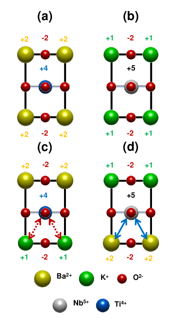
During the development of the model we assume a -type interface, simulated within an isolated slab geometry, with the non-polar material at the left and the polar material (with a formal ionic charge of alternating from layer to layer, where is the magnitude of the electronic charge) at the right [see Fig. 1(a)]. The generalization for other configurations is straightforward, changing the appropriate signs when required.
Within the modern theory of polarization, we can compute the “formal” bulk polarization from the positions of the atomic nuclei and the center of localized Wannier functions. This decomposition of the charge (nuclear and electronic) into localized contributions allows for a simple classical interpretation of the bulk polarization in terms of a point charge model, and rescue the Clausius-Mossotti formulation.
In the perfectly ideal structure without rumpling, where an atomically sharp junction in the absence of defects is supposed, all the atoms at a given layer lie at the same plane [Fig. 1(a)]. Then, we can always choose unit cells that tile the crystal under appropriate primitive translations, and that leave the left-over interface region charge neutral. Stengel and Vanderbilt (2009) (It is important to note that, for the moment, we are assuming that the thickness of the polar layer is below the critical thickness for the formation of the 2DEG.) Then, the magnitude of the dipole of an individual (AO)-(BO2) unit in this material is , where is the out-of-plane lattice constant. The sign of the dipole is always directed from the negative to the positive layer, so in the considered configuration the sign is negative [see Fig. 1(a)]. This dipole corresponds to a “built-in formal” polarization (calculated for the previous choice of unit cell for the primitive basis of atoms and Wannier functions) of
| (1) |
where is the volume of the unit cell of the polar material and is the cell surface. Analogously, since the layers are formally charged neutral in the non-polar material, .
Now, we can wonder what would happen if the materials that constitute the interface are ferroelectric, with a non-vanishing ferroelectric contribution to the polarization (this might be also the case when a compressive epitaxial strain is applied to the SrTiO3/LaAlO3 interface Bark et al. (2011)). In this situation, the ferroelectric polarization must be added to the “built-in” polarization of the polar layer. Stengel (2011)
The difference in the polarization at the interface between the two materials produces a surface density of bound charge,
| (2) |
Classical electromagnetic theory (Gauss’s theorem) teaches us that this sheet of interfacial charge gives rise to a change in the macroscopic electric field in the two materials of
| (3) |
where is the dielectric permittivity of vacuum [Fig. 1(b)]. The exact magnitude of the fields depends on the electrostatic boundary conditions, extremely linked with the geometry of the simulation boxes used in the computations (see Supplemental Material of Ref. Stengel, 2011 for a complete review).
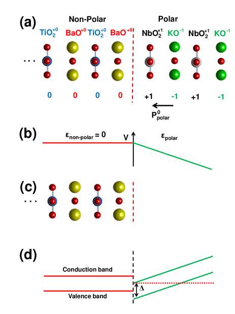
The field might induce strong structural changes in the materials and polarizes the electronic Wannier functions. Both facts translate into the development of a field-induced polarization [Fig. 1(c)] that tends to screen the discontinuity of the total polarization ,
| (4) |
and, consequently, of the macroscopic electric field. At the end, a self-consistent solution of Eqs. (2)-(4) is achieved where the polarizations in the two materials are in equilibrium with the corresponding macroscopic electric fields, and the total energy of the system is minimized.
For a sufficiently thin polar layer thickness, before the electronic reconstruction takes place, the absence of free charge at the interface requires the normal component of the electric displacement field to be preserved,
| (5) |
The finite electric displacement is an input parameter of the model. In a first-principles simulations its value can be set by hand using the virtual crystal approximation to introduce external fractional charges in the surface atoms layers, while constraining the macroscopic electric field to be strictly zero in the vacuum region. Stengel (2011) Other authors fix the atomic positions on the surface unit cell to some specific values. Bark et al. (2011)
From the definition of the electric displacement field,
| (6) |
and assuming that the polar material behaves as a linear dielectric of susceptibility around the spontaneous polarization structure, then
| (7) |
and Eq. (6) transforms into
| (8) |
| (9) |
This electric field tilts the electronic bands of the polar layer [Fig. 1(d)]. At a given critical thickness, , the top of the valence band of the polar material reaches the level of the bottom of the conduction bands. Reinle-Schmitt et al. (2011) Beyond , a Zener breakdown takes place, with the concomitant transfer of charge from the surface of the polar material to the interface. The magnitude of can be easily computed from Eq. (9) as
| (10) |
where is the interfacial potential step. will depend on the type of band alignment and on the particular interface ( or ). Here, according to the band alignment of Fig. 1(d) for the interface is given by Del
| (11) |
where is the band-gap of the polar material. Note that the band alignment in our interfaces, where the band gaps of BaTiO3 and KNbO3 are very similar, is of type II, different from that in the prototypical LaAlO3/SrTiO3 case (type I). For schematic views of the types of interfaces according to the band offset see Ref. wik, .
The first conclusion that can be drawn from Eq. (10) is that the polarizability of the polar layer is essential to determine the critical thickness for the formation of the 2DEG (it is directly proportional to ). The role played by the polar distortions to avoid the polar catastrophe in LaAlO3/SrTiO3 interfaces has been confirmed by first-principles simulations. Pentcheva and Pickett (2009) The importance of the extra screening due to lattice relaxations has also been discussed in the strongly related LaTiO3/SrTiO3 interfaces. Hamann et al. (2006); Okamoto et al. (2007); Larson et al. (2008) Indeed, the success for explaining the critical thickness for the formation of the 2DEG, Thiel et al. (2006); Lee and Demkov (2008); Chen et al. (2009) together with the electrostrictive effect on the polar LaAlO3 films, Cancellieri et al. (2011) are between the most important achievements of the polar discontinuity model.
The second conclusion is related with the relationship between and the ferroelectric polarization in the non-polar layer. In many works, the simulations try to reproduce the behavior of a thin polar layer on top of a thick non-polar substrate. In such cases, the macroscopic field in the non-polar materials is forced to be zero, either by symmetry or by using a dipole correction in vacuum. As a consequence, . If the ferroelectric contribution to the polarization in the non-polar layer points in the same direction as the “built-in” polarization in the polar one, then it contributes to increase the critical thickness. This has been proven in Ref. Bark et al., 2011 for the case of a SrTiO3/LaAlO3 interface subject to epitaxial strain [Eq. (10) is equivalent to Eq. (4) in Ref. Bark et al., 2011 taking into account that, in this particular system and ].
Finally, the third conclusion is that there is also a strong influence of an eventual spontaneous polarization of the polar material in the value of . In particular, if is close in magnitude to and points in the opposite direction, so the “built-in” polarization can be almost compensated by the ferroelectric contribution to the polarization, a large cancellation of the term in parentheses in the denominator of Eq. (10) is produced, with the concomitant increase in the critical thickness. In a previous work, Murray and Vanderbilt Murray and Vanderbilt (2009) have estimated how in SrTiO3/KNbO3 superlattices the system would not become metallic until the number of layers of KNbO3 is larger than 32.
To further validate Eq. (10) in an isolated slab geometry, we have carried out simulations on BaTiO3/KNbO3 interfaces. The motivation for this choice is four fold: (i) under appropriate compressive in-plane strains, KNbO3 is a ferroelectric polar material, with the spontaneous polarization pointing along the [001] direction, and with a “built-in” polarization of (value computed at the theoretical in-plane lattice constant of an hypothetical SrTiO3 substrate, = 3.874 Å), (ii) under this mechanical boundary condition, both KNbO3 and BaTiO3 can be stabilized with the same tetragonal symmetry, (iii) the theoretical spontaneous polarization of our tetragonal KNbO3 in bulk is , close to the built-in polarization, and (iv) we can also test to which extent the ferroelectric contribution to the polarization in the BaTiO3 layer is dominated by the imposed value of the displacement field in the simulations. First-principles results and comparison with the previous model will be presented in Sec. IV.
III Computational details
We have carried out density functional first-principles simulations based on a numerical atomic orbital method as implemented in the Siesta code. Soler et al. (2002) All the calculations have been carried out within the local density approximation (LDA), using the Perdew and Zunger Perdew and Zunger (1981) parametrization of the Ceperley and Alder functional Ceperley and Alder (1980) to simulate the electronic exchange and correlation. This choice avoids the systematic overestimation of the ferroelectric character Junquera and Ghosez (2008) of perovskite oxides found in other commonly used functionals Perdew et al. (1996) based on the generalized gradient approximation. This is an important point in this study, since the dielectric properties of the oxides at the bulk level might determine the behavior of the interfaces, in particular a tendency for “overscreening” of the 2DEG when the ferroelectric properties are favored. Stengel (2011)
Core electrons were replaced by ab-initio norm conserving pseudopotentials, generated using the Troullier-Martins scheme, Troullier and Martins (1991) in the Kleinman-Bylander fully non-local separable representation. Kleinman and Bylander (1982) Due to the large overlap between the semicore and valence states, the semicore and electrons of Ti, and electrons of K, and electrons of Nb, and and electrons of Ba were considered as valence electrons and explicitly included in the simulations. K, Ti, Nb and Ba pseudopotentials were generated scalar relativistically. The reference configuration and cutoff radii for each angular momentum shell for the pseudopotentials used in this work can be found in Ref. Junquera et al., 2003 for Ba, Ti, and O, and in Table 1 for K and Nb.
| K | Nb | ||
|---|---|---|---|
| Reference | |||
| Core radius | 1.50 | 1.45 | |
| 1.35 | 1.50 | ||
| 1.50 | 1.40 | ||
| 2.00 | 2.00 | ||
| Scalar relativistic? | yes | yes |
The one-electron Kohn-Sham eigenstates were expanded in a basis of strictly localized numerical atomic orbitals. Sankey and Niklewski (1989); Artacho et al. (1999) We used a single- basis set for the semicore states of K, Ti, Nb, and Ba and double- plus polarization for the valence states of all the atoms. For K (Ba), an extra shell of 3 (5) orbitals was added. All the parameters that define the shape and range of the basis functions were obtained by a variational optimization of the energy Junquera et al. (2001) in bulk cubic BaTiO3 (for Ba, Ti, and O), and of the entalphy Anglada et al. (2002) (with a pressure P = 0.03 GPa) in bulk cubic KNbO3 (for K and Nb, the basis set of O was frozen to that obtained in BaTiO3).
The electronic density, Hartree, and exchange correlation potentials, as well as the corresponding matrix elements between the basis orbitals, were calculated in a uniform real space grid. An equivalent plane wave cutoff of 1200 Ry was used to represent the charge density. For the Brillouin zone integrations we use a Monkhorst-Pack sampling Monkhorst and Pack (1976) equivalent to in a five atom perovskite unit cell.
To avoid the problem of artificially charging the interface with the use of non-stoichiometric superlattices with periodic boundary conditions, we follow the proposal of Lee and Demkov. Lee and Demkov (2008) Within this approach, the calculations were performed on vacuum-terminated (KNbO3)m/(BaTiO3)l/(KNbO3)m slabs, where the number of KNbO3 cells, , is always an integer number to guarantee the electrical neutrality of the interface. In particular, we have focused on two kinds of systems: symmetric slabs where both interfaces between BaTiO3 and KNbO3 are of the same kind (either -type TiO2/KO, or -type BaO/NbO2 interfaces), and asymmetric interfaces where one interface is TiO2/KO and the other BaO/NbO2. In both cases we have relaxed structures containing a different number of KNbO3 and BaTiO3 unit cells, given by the subscripts and , respectively. In the asymmetric interface a dipole slab correction is used to guarantee that the electric field in vacuum vanishes.
The in-plane lattice constant was fixed to the theoretical one of an hypothetical SrTiO3 substrate ( = 3.874 Å). Under this constraint, both BaTiO3 and KNbO3 are under conditions of compressive epitaxial strains. This will be relevant for the discussion of Sec. IV.2.
Starting from ideal reference structures, built by piling up the corresponding unit cells of bulk strained materials without rumpling, the atomic coordinates are relaxed until the maximum component of the force on any atom was smaller than 0.01 eV/Å. In the symmetric slabs, the minimization is performed in a two step process: First, mirror symmetry planes are imposed on the central layer of BaTiO3 to avoid the development of a polarization in any direction. Then, symmetry is broken displacing coherently the cations by hand, and a second relaxation is carried out without any imposed symmetry. In the asymmetric slabs, the relaxations are carried out in a single step, since the symmetry is broken directly in the initial reference structure.
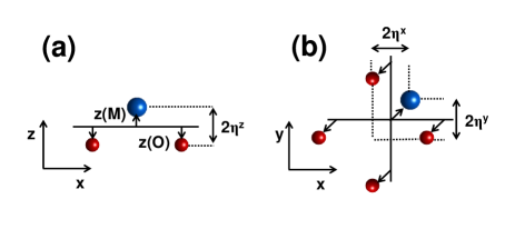
To stablish the notation, we will call the plane parallel to the interface the plane, whereas the perpendicular direction will be referred to as the -axis.
IV Results
IV.1 Out-of-plane lattice relaxations and screening
In order to characterize the atomic displacements induced by the relaxation, we define the “out-of-plane” rumpling parameter along of layer as , where and are, respectively, the coordinates of the cations and the oxygens at a given layer [Fig. 2(a)]. We also define the “in-plane” rumplings (), in an equivalent way, as represented graphically in Fig. 2(b).
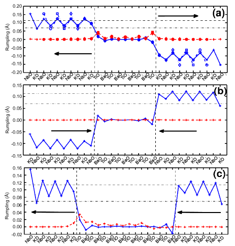
In all the studied systems a large out-of-plane rumpling is observed within the KNbO3 layers, with a magnitude that is essentially independent of their thickness and the kind of interface: symmetric [Fig. 3(a)], symmetric [Fig. 3(b)] or asymmetric [Fig. 3(c)]. Two oxide layers away from the interface, the layer-by-layer rumpling converges to a rather uniform sawtooth pattern, with values slightly larger than those observed in bulk KNbO3 under the same epitaxial conditions. This fact is consistent with , with tending to compensate for the difference in order to screen the polarization discontinuity at the interface. Only in the neighborhood of the free surface, a small deviation from this trend is obtained due to the larger relaxations on the surface atoms.
The dipole slab correction ensures that the displacement field in vacuum vanishes, . Due to the absence of surface external charges in the simulations, this value is preserved at the interfaces. This implies that a polarization in the BaTiO3 layer induces a depolarizing field that is responsible for a large electrostatic energy. Therefore, under this electrical boundary conditions, no polarization is expected on BaTiO3. Both facts are well reproduced in our simulations, where we observe that the out-of-plane polarization vanishes within the BaTiO3 layer in all cases. This happens even when the mirror symmetries are lifted by hand (in the symmetric interfaces), or spontaneously (in the asymmetric slabs).
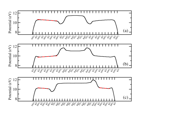
According to the model developed in Sec. II, the polarization in the polar layer tends to screen the discontinuity of the polarization at the interface and, therefore, its sign opposes that of the “formal” polarization. The lattice screening avoids the development of an electric field in the polar material that would result in the tilting of its bands and, for sufficiently large thicknesses, to a Zener breakdown and accumulation of charge at the interfaces. The lattice screening provided by KNbO3 is much stronger than the one anticipated in LaAlO3, where the structural distortion sustains the insulating behavior up to only 5 overlayers of LaAlO3 on SrTiO3. Pentcheva and Pickett (2009) As a consequence, in our simulations all the computed structures are insulating. The reason behind this is that the LaAlO3 is a wide band gap insulator with a low dielectric constant () and no ferroelectric instability ( =0). It costs some energy to polarize it. On the contrary, KNbO3 is a ferroelectric oxide that polarizes spontaneously and contributes to reduce the field [making smaller the numerator of Eq. (9)], and increase the critical thickness for the formation of the 2DEG [making larger the denominator of Eq. (10)]. The reduction of the internal field within KNbO3 can be directly checked from the nanosmoothed Colombo et al. (1991); Junquera et al. (2007) electrostatic potential in the slabs. Independently of the geometry, the magnitude of the field amounts to 0.024 eV/Å [see red dashed lines in Fig. 4] to be compared with the roughly constant electric field of 0.24 eV/Å (one order of magnitude larger) found in LaAlO3/SrTiO3 interfaces. Lee and Demkov (2008); Cancellieri et al. (2011) This is in very good agreement with the prediction of the electrostatic model developed in Sec. II: using a dielectric constant of bulk KNbO3 around the ferroelectric structure under the same mechanical boundary condition of 25.0, Ste Eq. (9) yields a value of 0.023 eV/Å.
Since the interfacial potential steps between KNbO3 and BaTiO3 are 1.08 eV for the TiO2/KO interface and 1.31 eV for the BaO/NbO2 interface (both values computed using the recipe given in Ref. Stengel et al., 2009 when the bands of one material are tilted), the estimated critical thickness to trigger the polar catastrophe under the condition of a vanishing electric displacement according to Eq. (10) are, respectively, 170 Å and 180 Å (between 42 and 44 unit cells), one order of magnitude larger than in LaAlO3/SrTiO3.
IV.2 In-plane polarization
Even though the ground state of bulk KNbO3 and BaTiO3 at zero temperature is rhombohedral, where the polarization displays both in-plane and out-of-plane () components, when a compressive in-plane strain is applied the polarization in the -directions is strongly reduced or even suppressed. Diéguez et al. (2004) In particular, when KNbO3 or BaTiO3 thin films are grown on top of a SrTiO3 substrate, the in-plane polarization of these materials vanishes and the tetragonal -phase is stabilized. Yoneda et al. (1998, 1998) However, contrary to current thought, in our calculations of the BaTiO3/KNbO3 interfaces, we can observe in Fig. 3 the appearance of a moderate in-plane polarization in these systems along the [110] direction. The layer-by-layer in-plane rumpling profile plotted in Fig. 3 reveals that the effect is highly localized at the -type TiO2/KO interface, quickly decaying upon moving into BaTiO3, and it is completely absent at the -type BaO/NbO2 interfaces.
The origin of the hidden interfacial in-plane polarization can be easily understood with a simple electrostatic model based on formally charged ions. In Fig. 5 we compare the atomic structure of bulk BaTiO3 [Fig. 5(a)] and KNbO3 [Fig. 5(b)] with that present in the -type TiO2/KO [Fig. 5(c)] and -type BaO/NbO2 [Fig. 5(d)] interfaces. The cleavage of bulk BaTiO3 and KNbO3 to form the -type TiO2/KO interface is accompanied by a change in the local electrostatic potential felt by the Ti cations. At the interface, some of the Ba cations (nominal charge +2) in the first neighbour atomic layer are replaced by K cations (nominal charge +1). This implies that at that interface the in-plane Ti cation movement is less constrained than in bulk, due to the reduced repulsions with K ions with respect to Ba ones. Analogously, in the -type interface the electrostatic potential felt by the Nb atoms is also altered. In this case the K+1 cations are replaced by Ba+2 ions, leading to an enhanced repulsion that hinders the appearance of any in-plane polarization. As this effect is directly related to the nominal charges of the ions in both interfacial materials we would expect it to be present in other similar systems and could be used to induce in-plane polarizations in other ferroelectric nanostructures.
To further characterize the development of the in-plane polarization, we take the relaxed coordinates of the asymmetric slab with = 5 and = 8 and remove by hand the in-plane displacements. We use this new structure as a reference configuration. Then, we compute the in-plane distortions required to go from the reference configuration to the relaxed structure and decompose into their and components. Finally, given fractions of these distortions are frozen in on top of the reference structure. The energy surface obtained for different fractions of the in-plane rumplings is represented in Fig. 6. From this energy landscape we can extract (i) the stabilization energy (the energy difference between the polar state and the reference one), that amounts to 43.5 meV/slab, and (ii) the energy barriers that prevents the system to rotate the in-plane polarization from [110] direction to any of the other symmetry-equivalent positions, passing through the transition state at [100] positions. This is only 16 meV, slightly larger than those found in artificial Ruddlesden-Popper-type superlattices. Nakhmanson and Naumov (2010) To gauge the magnitude of these barriers, we compare them with the rotation zero-point-energy (ZPE) in this slab. This value is obtained through the nuclear motion Hamiltonian
| (12) |
where is the energy represented in Fig. 6 and can be shown to be
| (13) |
by writing the kinetic energy operator expressed in terms of atomic coordinates and masses () using the linear trasformation relating the effective modes and with the atomic displacements through the coefficients . To solve the Schrödinger equation associated to Eq. (12) and find the vibrational levels associated to Fig. 6 we follow the recipe given in Ref. García-Fernández et al., 2010. Then, we compute the ZPE by comparing the position of the first level to the minimum of the energy surface. The resulting value for the ZPE, 13.6 meV, is much smaller than the global stabilization energy but comparable to the height of the rotational barrier, indicating that quantum fluctuations will be important in these nanostructures. These fluctuations prevent the observation of any in-plane spontaneous polarization, since the system will be delocalized over the four equivalent minima in [110] directions in a similar way to what happens in a dynamic Jahn-Teller problem. García-Fernández et al. (2010)
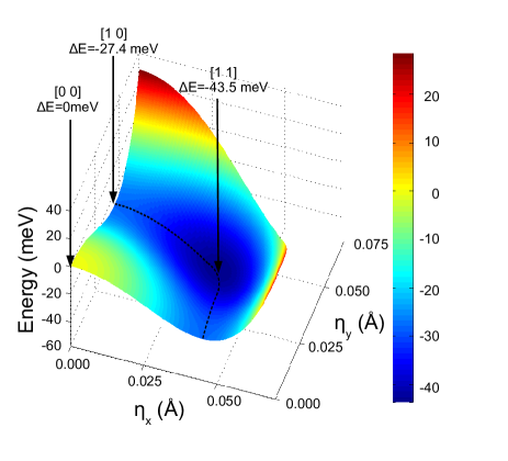
This case can be compared with what happens in an incipient ferroelectric. In the latter case quantum fluctuations make the ZPE larger than the double well stabilization energy making the maximum of the probability density associated to the distortion (and the polarization) to be localized at the centrosymmetric state (origin in Fig. 6). On the other hand, in the present case, the maximum of the probability density corresponds with a non-zero polarization region around the origin (see dashed line in Fig. 6) but directional averaging results in a null net polarization. However, the coherent dynamics between the wells could be disrupted by small electric fields along the plane, that would induce large changes in the directionality of the in-plane polarization. The signature of such potential energy surface for polarization rotation would be a high dielectric constant. Nakhmanson and Naumov (2010)
V Conclusions
In summary, using accurate first-principles simulations we have studied the influence of the ferroelectric polarization of the polar layer in the formation of 2DEG at BaTiO3/KNbO3 interfaces. The most important conclusions that can be drawn are: (i) the spontaneous polarization of the polar KNbO3 layer cancels out almost exactly the “built-in” polarization discontinuity at the interface; (ii) as a consequence of this compensation, the critical thickness for the formation of the 2DEG is estimated to be between 42 and 44 unit cells of KNbO3, one order of magnitude larger than in SrTiO3/LaAlO3 interfaces; (iii) this behavior can be easily explained in terms of a simple model based on the modern theory of polarization and basic electrostatics; and (iv) surprisingly, BaTiO3 displays an in-plane component of the polarization at the -type TiO2/KO interface, even when BaTiO3 is under in-plane compressive strains. However we do not expect this in-plane polarization to be experimentally observable as the barriers for its rotation are very small and quantum fluctuations will prevent it from being localized in a particular direction. This situation could be easily modified by the application of small electric fields that will break the symmetry and reveal the hidden polarization.
We thank Massimiliano Stengel for useful discussions and a critical reading of the manuscript. This work was supported by the Spanish Ministery of Science and Innovation through the MICINN Grant FIS2009-12721-C04-02, by the Spanish Ministry of Education through the FPU fellowship AP2006-02958 (PAP), and by the European Union through the project EC-FP7, Grant No. CP-FP 228989-2 “OxIDes”. The authors thankfully acknowledge the computer resources, technical expertise and assistance provided by the Red Española de Supercomputación. Calculations were also performed at the ATC group of the University of Cantabria.
References
- Ohtomo and Hwang (2004) A. Ohtomo and H. Y. Hwang, Nature (London), 427, 423 (2004).
- Mannhart et al. (2008) J. Mannhart, D. H. A. Blank, H. Y. Hwang, A. J. Millis, and J.-M. Triscone, MRS Bulletin, 33, 1027 (2008).
- Mannhart and Schlom (2010) J. Mannhart and D. G. Schlom, Science, 327, 1607 (2010).
- Brinkman et al. (2007) A. Brinkman, M. Huijben, M. van Zalk, J. Huijben, U. Zeitler, J. C. Maan, W. G. van der Wiel, G. Rijnders, D. H. A. Blank, and H. Hilgenkamp, Nature Mater., 6, 493 (2007).
- Reyren et al. (2007) N. Reyren, S. Thiel, A. D. Caviglia, L. F. Kourkoutis, G. Hammerl, C. Richter, C. W. Schneider, T. Kopp, A. S. Rüetschi, D. Jaccard, M. Gabay, D. A. Muller, J. M. Triscone, and J. Mannhart, Science, 317, 1196 (2007).
- Li et al. (2011) L. Li, C. Richter, S. Paetel, J. Mannhart, and R. C. Ashoori, Science, 332, 825 (2011).
- Gardner et al. (2011) H. J. Gardner, A. Kumar, L. Yu, P. Xiong, M. P. Warusawithana, L. Wang, O. Vafek, and D. G. Schlom, Nature Physics, 7, 895 (2011).
- Cen et al. (2009) C. Cen, S. Thiel, J. Mannhart, and J. Levy, Science, 323, 1026 (2009).
- Nakagawa et al. (2006) N. Nakagawa, H. Y. Hwang, and D. Muller, Nature Mater., 5, 204 (2006).
- Stengel and Vanderbilt (2009) M. Stengel and D. Vanderbilt, Phys. Rev. B, 80, 241103(R) (2009).
- Willmott et al. (2007) P. R. Willmott, S. A. Pauli, R. Herger, C. M. Schlepütz, D. Martoccia, B. D. Patterson, B. Delley, R. Clarke, D. Kumah, C. Cionca, and Y. Yacoby, Phys. Rev. Lett., 99, 155502 (2007).
- Herranz et al. (2007) G. Herranz, M. Basletić, M. Bibes, C. Carrétéro, E. Tafra, E. Jacquet, K. Bouzehouane, C. Deranlot, A. Hamzić, J.-M. Broto, A. Barthélémy, and A. Fert, Phys. Rev. Lett., 98, 216803 (2007).
- Kalabukhov et al. (2007) A. Kalabukhov, R. Gunnarsson, J. Borjesson, E. Olsson, T. Claeson, and D. Winkler, Phys. Rev. B, 75, 121404(R) (2007).
- Bristowe et al. (2011) N. C. Bristowe, P. B. Littlewood, and E. Artacho, Phys. Rev. B, 83, 205405 (2011).
- Cen et al. (2008) C. Cen, S. Thiel, G. Hammerl, C. W. Schneider, K. E. Andersen, C. S. Hellberg, J. Mannhart, and J. Levy, Nature Matter., 7, 298 (2008).
- Soon et al. (2010) W.-J. Soon, E. Cho, J. Lee, and S. Han, J. Phys.: Condens. Matter, 22, 315501 (2010).
- Thiel et al. (2006) S. Thiel, G. Hammerl, A. Schmehl, C. W. Schneider, and J. Mannhart, Science, 313, 1942 (2006).
- Hotta et al. (2007) Y. Hotta, T. Susaki, and H. Y. Hwang, Phys. Rev. Lett., 99, 236805 (2007).
- Huijben et al. (2006) M. Huijben, G. Rijnders, D. H. A. Blank, S. Bals, S. V. Aert, J. Verbeeck, G. V. Tendeloo, A. Brinkman, and H. Hilgenkamp, Nature Mater., 5, 204 (2006).
- Chen et al. (2009) H. Chen, A. M. Kolpak, and S. Ismail-Beigi, Phys. Rev. B, 79, 161402(R) (2009).
- Oja and Nieminen (2009) R. Oja and R. M. Nieminen, Phys. Rev. B, 80, 205420 (2009).
- Oja et al. (2012) R. Oja, M. Tyunina, L. Yao, T. Pinomaa, T. Kocourek, A. Dejneka, O. Stupakov, M. Jelinek, V. Trepakov, S. van Dijken, and R. M. Nieminen, Phys. Rev. Lett., 109, 127207 (2012).
- Niranjan et al. (2009) M. K. Niranjan, Y. Wang, S. S. Jaswal, and E. Y. Tsymbal, Phys. Rev. Lett., 103, 016804 (2009).
- Wang et al. (2009) Y. Wang, M. K. Niranjan, S. S. Jaswal, and E. Y. Tsymbal, Phys. Rev. B, 80, 165130 (2009).
- Stengel (2011) M. Stengel, Phys. Rev. B, 84, 205432 (2011a).
- Lee and Demkov (2008) J. Lee and A. A. Demkov, Phys. Rev. B, 78, 193104 (2008).
- Resta and Vanderbilt (2007) R. Resta and D. Vanderbilt, “Physics of ferroelectrics: a modern perspective,” (Topics of Applied Physics, Springer, Berlin, 2007) pp. 31–68.
- Stengel (2011) M. Stengel, Phys. Rev. Lett., 106, 136803 (2011b).
- Bark et al. (2011) C. W. Bark, D. A. Felker, Y. Wang, Y. Zhang, H. W. Jang, C. M. Folkman, J. W. Park, S. H. Baek, H. Zhou, D. D. Fong, Z. Q. Pan, E. Y. Tsymbal, M. S. Rzchowski, and C. B. Eom, PNAS, 108, 4720 (2011).
- Reinle-Schmitt et al. (2011) M. L. Reinle-Schmitt, C. Cancellieri, D. Li, D. Fontaine, M. Medarde, E. Pomjakushina, C. W. Schneider, S. Gariglio, Ph. Ghosez, J. M. Triscone, and P. R. Willmott, (2011).
- (31) For a interface of type II, , where is the conduction band minimum of the corresponding layer right at the interface.
- (32) See http://en.wikipedia.org/wiki/Heterojunction.
- Pentcheva and Pickett (2009) R. Pentcheva and W. E. Pickett, Phys. Rev. Lett., 102, 107602 (2009).
- Hamann et al. (2006) D. R. Hamann, D. A. Muller, and H. Y. Hwang, Phys. Rev. B, 73, 195403 (2006).
- Okamoto et al. (2007) S. Okamoto, A. J. Millis, and N. A. Spaldin, Phys. Rev. Lett., 97, 056802 (2006).
- Larson et al. (2008) P. Larson, Z. S. Popovic, and S. Satpathy, Phys. Rev. B, 77, 245122 (2008).
- Cancellieri et al. (2011) C. Cancellieri, D. Fontaine, S. Gariglio, N. Reyren, A. D. Caviglia, A. Féte, S. J. Leake, S. A. Pauli, P. R. Willmott, M. Stengel, Ph. Ghosez, and J.-M. Triscone, Phys. Rev. Lett., 107, 056102 (2011).
- Murray and Vanderbilt (2009) E. D. Murray and D. Vanderbilt, Phys. Rev. B, 79, 100102(R) (2009).
- Soler et al. (2002) J. M. Soler, E. Artacho, J. D. Gale, A. García, J. Junquera, P. Ordejón, and D. Sánchez-Portal, J. Phys.: Condens. Matter, 14, 2745 (2002).
- Perdew and Zunger (1981) J. P. Perdew and A. Zunger, Phys. Rev. B, 23, 5048 (1981).
- Ceperley and Alder (1980) D. M. Ceperley and B. J. Alder, Phys. Rev. Lett., 45, 566 (1980).
- Junquera and Ghosez (2008) J. Junquera and Ph. Ghosez, J. Comput. Theor. Nanosci., 5, 2071 (2008).
- Perdew et al. (1996) J. P. Perdew, K. Burke, and M. Ernzerhof, Phys. Rev. Lett., 77, 3865 (1996).
- Troullier and Martins (1991) N. Troullier and J. L. Martins, Phys. Rev. B., 43, 1993 (1991).
- Kleinman and Bylander (1982) L. Kleinman and D. M. Bylander, Phys. Rev. Lett., 48, 1425 (1982).
- Junquera et al. (2003) J. Junquera, M. Zimmer, P. Ordejón, and Ph. Ghosez, Phys. Rev. B, 67, 155327 (2003).
- Sankey and Niklewski (1989) O. F. Sankey and D. J. Niklewski, Phys. Rev. B, 40, 3979 (1989).
- Artacho et al. (1999) E. Artacho, D. Sánchez-Portal, P. Ordejón, A. García, and J. M. Soler, Phys. Stat. Sol. (b), 215, 809 (1999).
- Junquera et al. (2001) J. Junquera, O. Paz, D. Sánchez-Portal, and E. Artacho, Phys. Rev. B, 64, 235111 (2001).
- Anglada et al. (2002) E. Anglada, J. M. Soler, J. Junquera, and E. Artacho, Phys. Rev. B, 66, 205101 (2002).
- Monkhorst and Pack (1976) H. J. Monkhorst and J. D. Pack, Phys. Rev. B, 13, 5188 (1976).
- Colombo et al. (1991) L. Colombo, R. Resta, and S. Baroni, Phys. Rev. B, 44, 5572 (1991).
- Junquera et al. (2007) J. Junquera, M. H. Cohen, and K. M. Rabe, J. Phys.: Condens. Matter, 19, 213203 (2007).
- (54) Massimiliano Stengel, private communication.
- Stengel et al. (2009) M. Stengel, D. Vanderbilt, and N. A. Spaldin, Phys. Rev B, 80, 224110 (2009).
- Diéguez et al. (2004) O. Diéguez, S. Tinte, A. Antons, C. Bungaro, J. B. Neaton, K. M. Rabe, and D. Vanderbilt, Phys. Rev. B, 69, 212101 (2004).
- Yoneda et al. (1998) Y. Yoneda, T. Okabe, K. Sakaue, H. Tekauchi, H. Kasatani, and K. Deguchi, J. Appl. Phys., 83, 2458 (1998a).
- Yoneda et al. (1998) Y. Yoneda, T. Okabe, K. Sakaue, and H. Tekauchi, Surf. Sci., 410, 62 (1998b).
- Nakhmanson and Naumov (2010) S. M. Nakhmanson and I. Naumov, Phys. Rev. Lett., 104, 097601 (2010).
- García-Fernández et al. (2010) P. García-Fernández, A. Trueba, M. T. Barriuso, J. A. Aramburu, and M. Moreno, Phys. Rev. Lett., 104, 035901 (2010).