Semimetal-to-Antiferromagnetic Insulator Transition in Graphene Induced by Biaxial Strain
Abstract
We report first-principles calculations on the antiferromagnetic spin ordering in graphene under biaxial strain. Using hybrid functional calculations, we found that the semimetallic graphene sheets undergo a transition to antiferromagnetic insulators at a biaxial strain of 7.7% and that the band gap rapidly increases after the onset of this transition before reaching 0.9 eV at a biaxial strain of 12%. We examined the competition of the antiferromagnetic spin ordering with two-dimensional Peierls distortions upon biaxial strain, and found that the preceding antiferromagnetic insulator phase impedes the Peierls insulator phase. The antiferromagnetic insulator phase is destabilized upon carrier filling but robust up to moderate carrier densities. This work indicates that biaxially strained graphene represents a noble system where the electron-electron and electron-lattice interactions compete with each other in a simple but nontrivial way.
I Introduction
Graphene, which consists of a honeycomb lattice of carbon atoms, exhibits a high carrier mobility and is appealing for electronic applications, such as channel materials for field-effect transistors.Novoselov et al. (2005); Zhang et al. (2005) A crucial obstacle for the potential applications of graphene is its absence of a band gap, which results in poor on–off current ratios in a transistor.Schwierz (2010) The introduction of a band gap or a metal-to-insulator transition in semimetallic graphene can greatly enhance its utility.
Graphene is a semimetal with an eight-fold degeneracy at its intrinsic Fermi level, which originates from three twofold symmetries of sublattices, valleys, and spins.Castro Neto et al. (2009) Therefore, opening the band gap requires breakage of the symmetries or mixing of the degenerate states. The gap opening in graphene on SiC substrates Zhou et al. (2007) is induced by sublattice symmetry breaking,Semenoff (1984) which results in an asymmetric charge population in two sublattices of the honeycomb lattice. The degeneracy from two inequivalent Dirac valleys at and can be lifted by intervalley mixing potentials with a real-space periodicity of .Mañes et al. (2007); Chamon (2000) The gap opening in graphene with periodic adsorbates Balog et al. (2010) or holes Pedersen et al. (2008); Kim et al. (2010) and in armchair-edge graphene nanoribbons Barone et al. (2006); Son et al. (2006); Han et al. (2007) belongs to this category.Lee et al. (2011) Recently, we have shown Lee et al. (2011) that gap opening by intervalley mixing occurs in biaxially strained graphene through spontaneous inverse-Kekulé distortions that produce potential modulations of the periodicity rather than through external modulations. However, this two-dimensional Peierls metal–insulator transition is accompanied by structural failure.Lee et al. (2011); Marianetti and Yevick (2010) The physical origin of the gap opening under biaxial strain is distinct from that under uniaxial strain Pereira et al. (2009); Pereira and Castro Neto (2009); Choi et al. (2010) or inhomogeneous strain,Guinea et al. (2009) which breaks local hexagonal symmetries to induce Dirac-point merging or pseudo-Landau level formation, respectively. As the last category, the gap opening in zigzag-edge graphene nanoribbons involves breaking of the spin symmetry by the formation of ferrimagnetic spin ordering at the edges.Fujita et al. (1996); Son et al. (2006)
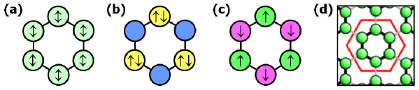
In this work, we investigate the possibility of spin ordering in graphene, not just at edges, but throughout the two-dimensional sheet. The honeycomb lattice, which is composed of two triangular sublattices, can support unfrustrated antiferromagnetism and can have an antiferromagnetic ground state with a finite band gap when the onsite electron–electron Coulomb energy, , is high compared to the electronic hopping integral, .Sorella and Tosatti (1992) The critical value of for the antiferromagnetic spin ordering has been predicted to be according to quantum Monte Carlo calculations based on the Hubbard model.Sorella and Tosatti (1992); Martelo et al. (1997); Furukawa (2001); Meng et al. (2010) In Fig. 1, the electronic ordering of the antiferromagnetic insulator phase is compared to those of the other gap-opening orderings. The antiferromagnetic insulator phase also breaks the sublattice symmetry; however, in this case, the symmetry breaking involves spin ordering, not charge ordering. Graphene, whose electronic structure is characterized by the honeycomb lattice of C states, has a zero band gap with no magnetic ordering because the relative onsite Coulomb energy is subcritical.Yazyev (2010); Wehling et al. (2011) The ferrimagnetic ordering at the zigzag edges can be attributed to a local increase in the effective at the edges by reduced bonding configurations. A homogeneous increase in can be achieved if the atomic distances are uniformly increased, e.g., through the application of biaxial strain.
In this study, we used first-principles calculations to examine the onset and stability of the antiferromagnetic insulator phase in biaxially strained graphene. Our hybrid functional calculations showed that the semimetal-to-antiferromagnetic insulator transition occurs at a biaxial strain of 7.7% and that the band gap rapidly increases after the onset of this transition before reaching 0.9 eV at a biaxial strain of 12%. We also examined the competition of the antiferromagnetic spin ordering with two-dimensional Peierls distortions upon biaxial strain, and found that the preceding antiferromagnetic insulator phase impedes the Peierls insulator phase. Our calculations on the effect of carrier filling showed that the antiferromagnetic insulator phase is destabilized upon carrier filling but robust up to moderate carrier densities.
II Method
To study the antiferromagnetic spin ordering, we performed hybrid functional calculations Heyd et al. (2003) in which the exact Hartree–Fock (HF) exchange energy was hybridized with the exchange-correlation energy from the generalized gradient approximation (GGA) within the framework of a generalized Kohn–Sham scheme Seidl et al. (1996) to remedy the self-interaction error of the GGA calculations.Kudin et al. (2002) Hybrid functional calculations have been used to describe the electronic structures of traditional and antiferromagnetic Mott insulators, such as NiO, MnO, VO2, and UO2.Kudin et al. (2002); Marsman et al. (2008); Archer et al. (2011); Eyert (2011); Grau-Crespo et al. (2012)
Our hybrid functional calculations employ the hybrid functional of Heyd, Scuseria, and Ernzerhof Heyd et al. (2003) and the projector-augmented-wave method, as implemented in VASP.Kresse and Furthmüller (1996); Kresse and Joubert (1999) Valence electronic wavefunctions are expanded in a plane-wave basis set with a cutoff energy of 400 eV. In our supercell calculations, the graphene layers are separated by 10 Å. The k-point integration was performed at a uniform k-point mesh of () in the Brillouin zone of the cell. The atomic positions are relaxed until the residual forces become less than 0.001 eV/Å. Our methods predict the band gaps of diamonds and hexagonal BN sheets to be 4.8 eV and 4.5 eV, respectively, compared to the experimentally obtained values of 5.5 eV and 5.2 eV, respectively.
III Results and Discussion
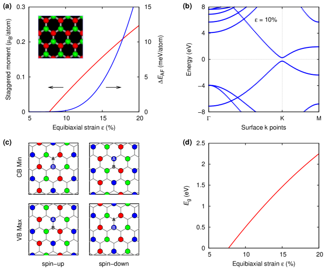
We examined the semimetal-to-antiferromagnetic insulator transition in graphene by increasing the lattice constant from a calculated equilibrium value. The antiferromagnetic phase becomes stable over the nonmagnetic phase at the relative increase in the lattice constant, or at an equibiaxial strain, , of % (Fig. 2a). The band structure after the transition (Fig. 2b) exhibits a gap at the point. Here, each of the energy bands is doubly degenerate, which corresponds to spin-up and spin-down components. The electronic wavefunctions of the two spin components (Fig. 2c) reveal contrasting spatial populations. The electronic states of the valence bands exhibit a preferential occupation of the spin-up component at the A sublattice and that of the spin-down component at the B sublattice, which accounts for the antiferromagnetic spin ordering. For the conduction bands, the spatial occupation is reversed for the two spin components. The calculated band gap (Fig. 2d) exhibits an almost identical dependence on with the staggered magnetic moment (Fig. 2a), which clearly reveals the correlation between the spin ordering and the band-gap opening.
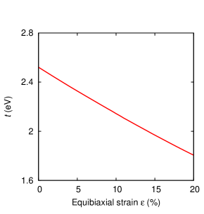
The transition to the antiferromagnetic insulator phase can be attributed to the reduction of the hopping integral, . The early onset of the antiferromagnetic insulator phase at % in graphene is remarkable because the typically accepted value of for pristine graphene, ,Yazyev (2010) is considerably smaller than , and the hopping integral, , only decreases by % at % (See Fig. 3). However, a recent evaluation Wehling et al. (2011) of the Coulomb interaction through a combination of first-principles calculations and a many-body formulation revealed that the of pristine graphene is as large as 3.3 and increases to at %. The present hybrid functional calculations support the large value of .
Because biaxially strained graphene can also exhibit a band gap opening as a spontaneous two-dimensional Peierls transition,Lee et al. (2011) we studied the competition of the antiferromagnetic insulator phase with the Peierls insulator phase. Peierls dimerization always occurs in one-dimensional atomic chains, irrespective of the force constant of atomic bonds.Peierls (1955) However, in two-dimensional lattices, such as the honeycomb lattice, this dimerization can only occur if the force constant is relatively small compared to the electronic hopping integral, .Mintmire et al. (1992) In pristine graphene, strong planar bonds hinder the Peierls distortion. However, biaxial strain rapidly weakens the bonds and results in the Kekulé or inverse-Kekulé distortion,Lee et al. (2011) which has been recently shown to be the unique Peierls dimerization mode for graphene sheets in the thermodynamic limit.Frank and Lieb (2011)
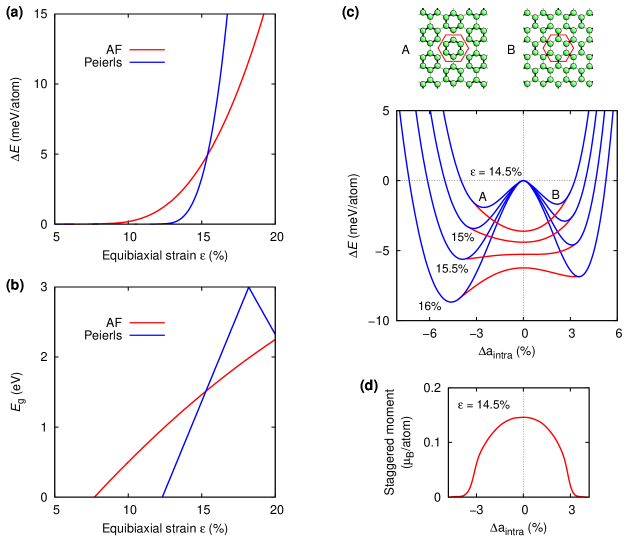
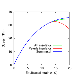
Our nonmagnetic calculations reveal an onset of the spontaneous inverse-Kekulé distortion at % (Fig. 4a). Above this onset, the band gap rapidly increases to a maximum of 3.0 eV at % (Fig. 4b), where the band begins to decrease below the empty band. Given the use of hybrid functional calculations in the present work, this result is consistent with previous GGA calculations,Lee et al. (2011) where the critical is 14.2% with the maximum band gap of 2.1 eV. The structural failure induced by this Peierls ordering, as predicted in previous works,Lee et al. (2011); Marianetti and Yevick (2010) occurs at (See Fig. 5). Compared to the antiferromagnetic insulator phase that initiates at %, this Peierls insulator phase exhibits a delayed onset but also exhibit a faster increase in the energy gain and band gap (Figs. 4a&b).
To understand the competition between the antiferromagnetic and Peierls insulator phases, we calculate energy profiles as a function of lattice distortion with the magnetic ordering on and off. At %, nonmagnetic calculations reveal a double-well energy profile (Fig. 4c) with two local minima that correspond to the stable structures of the inverse-Kekulé and Kekulé distortions, respectively, and a central maximum that corresponds to the undistorted structure. The inverse-Kekulé distortion (A, in Fig. 4c), where a six-membered ring structure similar to benzene is formed, is more stable than the Kekulé distortion (B, in Fig. 4c), which is characterized by ordered carbon dimers. When is increased, both energy minima deepen, and the stability of the inverse-Kekulé structure increases over the Kekulé structure.
When the antiferromagnetic ordering is turned on, the double-well energy profile changes to a single-well energy profile through a significant energy lowering of the undistorted structure (Fig. 4c). The calculated staggered magnetic moment (Fig. 4d) indicates that the antiferromagnetic ordering is maximal in the undistorted structure and is suppressed near the local minima of the Peierls ordering, which reflects the different symmetries of the two orderings. When is increased, the single-well energy profile becomes flatter, and, at the crossing point where %, the minimum moves continuously from the antiferromagnetic undistorted structure to the nonmagnetic inverse-Kekulé structure. Therefore, the single-well energy profile for % indicates that the antiferromagnetic insulator phase impedes the manifestation of the Peierls ordering and thereby slightly improves the mechanical stability of graphene under biaxial strain.
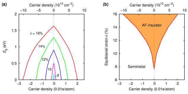
The stability of the antiferromagnetic insulator phase for assumes a half-filling of the band. The addition of charge carriers by filling the conduction bands or emptying the valence bands reduces the spin asymmetry at each atomic site, which reduces the band gap. For the potential use of biaxially strained graphene for field-effect transistors,Schwierz (2010) the behavior of this filling-control metal–insulator transitionImada et al. (1998) is important because graphene has nonzero minimum carrier densities of 1010–1012 cm-2 because of electron or hole puddles formed by charged defects or ripples.Martin et al. (2008); Adam et al. (2007) The calculated band gap with variable carrier filling (Fig. 6a) exhibits a maximum at the half-filling condition and a bell-shaped decrease upon the deviation from the maximum. The initial decrease of the band gap upon deviation from the half-filling condition reduces as increases. Therefore, at , the carrier filling of 1012 cm-2 decreases the band gap by eV, which indicates that the antiferromagnetic insulator phase is quite stable upon carrier filling of practical situations. Figure 6b summarizes the antiferromagnetic metal–insulator transition in graphene as a function of equibiaxial strain and carrier filling.
Finally we remark on the accuracy of our calculations in predicting the antiferromagnetic order. In the hybrid functional of Heyd, Scuseria, and Ernzerhof Heyd et al. (2003) used in this work, the exchange energy is described by a 25% HF exchange energy in combination with a 75% GGA exchange energy. Calculations using such a mixing parameter reasonably predict structural properties and band gaps of many inorganic materialsMarsman et al. (2008), but show a tendency to overestimate the antiferromagnetic coupling.Grau-Crespo et al. (2012) On the other hand, for organic materials and graphene nanostructures, they underestimate band gaps and incorrectly predict carrier localization.Jain et al. (2011); Sai et al. (2011) Reasonable band-gap values were empirically obtained for organic systems by taking the mixing parameter as the inverse of the dielectric constant of the material.Marques et al. (2011) The dielectric constant of graphene, which is , as determined from many-body perturbation calculationsWehling et al. (2011); van Schilfgaarde and Katsnelson (2011) suggests that the proper HF contribution for graphene could be as high as 40%, enhancing the antiferromagnetic coupling. Further studies are necessary to clarify this issue.
IV Conclusion
We have shown, using hybrid functional calculations, that biaxial strain can introduce a semimetal-to-antiferromagnetic insulator transition in two-dimensional graphene sheets. The transition occurs before the two-dimensional Peierls transition and thereby secures a margin before structural failure. This transition is robust upon finite carrier filling of practical situations. This work indicates that the application of biaxial strain provides a useful means to manipulate the electronic properties of graphene and could be exploited for electronic and spintronic device applications. From a fundamental perspective, our analysis of the competition between the antiferromagnetic ordering and the Peierls ordering in graphene provides an understanding of how the competition in an elemental linear atomic chain extends in two dimensions.
Acknowledgements.
The authors thank Ji Hoon Shim and Jongseob Kim for helpful discussions.References
- Novoselov et al. (2005) K. S. Novoselov, A. K. Geim, S. V. Morozov, D. Jiang, M. I. Katsnelson, I. V. Grigorieva, S. V. Dubonos, and A. A. Firsov, Nature 438, 197 (2005).
- Zhang et al. (2005) Y. Zhang, Y.-W. Tan, H. L. Stormer, and P. Kim, Nature 438, 201 (2005).
- Schwierz (2010) F. Schwierz, Nature Nanotech. 5, 487 (2010).
- Castro Neto et al. (2009) A. H. Castro Neto, F. Guinea, N. M. R. Peres, K. S. Novoselov, and A. K. Geim, Rev. Mod. Phys. 81, 109 (2009).
- Zhou et al. (2007) S. Y. Zhou, G.-H. Gweon, A. V. Fedorov, P. N. First, W. A. de Heer, D.-H. Lee, F. Guinea, A. H. C. Neto, and A. Lanzara, Nature Mater. 6, 770 (2007).
- Semenoff (1984) G. W. Semenoff, Phys. Rev. Lett. 53, 2449 (1984).
- Mañes et al. (2007) J. L. Mañes, F. Guinea, and M. A. H. Vozmediano, Phys. Rev. B 75, 155424 (2007).
- Chamon (2000) C. Chamon, Phys. Rev. B 62, 2806 (2000).
- Balog et al. (2010) R. Balog, B. Jørgensen, L. Nilsson, M. Andersen, E. Rienks, M. Bianchi, M. Fanetti, E. Lægsgaard, A. Baraldi, S. Lizzit, et al., Nature Mater. 9, 315 (2010).
- Pedersen et al. (2008) T. G. Pedersen, C. Flindt, J. Pedersen, N. A. Mortensen, A.-P. Jauho, and K. Pedersen, Phys. Rev. Lett. 100, 136804 (2008).
- Kim et al. (2010) M. Kim, N. S. Safron , E. Han, M. S. Arnold, and P. Gopalan, Nano Lett. 10, 1125 (2010).
- Barone et al. (2006) V. Barone, O. Hod, and G. E. Scuseria, Nano Lett. 6, 2748 (2006).
- Son et al. (2006) Y.-W. Son, M. L. Cohen, and S. G. Louie, Phys. Rev. Lett. 97, 216803 (2006).
- Han et al. (2007) M. Y. Han, B. Özyilmaz, Y. Zhang, and P. Kim, Phys. Rev. Lett. 98, 206805 (2007).
- Lee et al. (2011) S.-H. Lee, H.-J. Chung, J. Heo, H. Yang, J. Shin, U.-I. Chung, and S. Seo, ACS Nano 5, 2964 (2011).
- Marianetti and Yevick (2010) C. A. Marianetti and H. G. Yevick, Phys. Rev. Lett. 105, 245502 (2010).
- Pereira et al. (2009) V. M. Pereira, A. H. Castro Neto, and N. M. R. Peres, Phys. Rev. B 80, 045401 (2009).
- Pereira and Castro Neto (2009) V. M. Pereira and A. H. Castro Neto, Phys. Rev. Lett. 103, 046801 (2009).
- Choi et al. (2010) S.-M. Choi, S.-H. Jhi, and Y.-W. Son, Phys. Rev. B 81, 081407 (2010).
- Guinea et al. (2009) F. Guinea, M. I. Katsnelson, and A. K. Geim, Nature Phys. 6, 30 (2009).
- Fujita et al. (1996) M. Fujita, K. Wakabayashi, K. Nakada, and K. Kusakabe, J. Phys. Soc. Jpn. 65, 1920 (1996).
- Sorella and Tosatti (1992) S. Sorella and E. Tosatti, Europhys. Lett. 19, 699 (1992).
- Martelo et al. (1997) L. M. Martelo, M. Dzierzawa, L. Siffert, and D. Baeriswyl, Z. Phys. B 103, 335 (1997).
- Furukawa (2001) N. Furukawa, J. Phys. Soc. Jpn. 70, 1483 (2001).
- Meng et al. (2010) Z. Y. Meng, T. C. Lang, S. Wessel, F. F. Assaad, and A. Muramatsu, Nature 464, 847 (2010).
- Yazyev (2010) O. V. Yazyev, Rep. Prog. Phys. 72, 056501 (2010).
- Wehling et al. (2011) T. O. Wehling, E. Şaşıoğlu, C. Friedrich, A. I. Lichtenstein, M. I. Katsnelson, and S. Blügel, Phys. Rev. Lett. 106, 236805 (2011).
- Heyd et al. (2003) J. Heyd, G. E. Scuseria, and M. Ernzerhof, J. Chem. Phys. 118, 8207 (2003).
- Seidl et al. (1996) A. Seidl, A. Görling, P. Vogl, J. A. Majewski, and M. Levy, Phys. Rev. B 53, 3764 (1996).
- Kudin et al. (2002) K. N. Kudin, G. E. Scuseria, and R. L. Martin, Phys. Rev. Lett. 89, 266402 (2002).
- Marsman et al. (2008) M. Marsman, J. Paier, A. Stroppa, and G. Kresse, J. Phys.: Condens. Matter 20, 064201 (2008).
- Archer et al. (2011) T. Archer, C. D. Pemmaraju, S. Sanvito, C. Franchini, J. He, A. Filippetti, P. Delugas, D. Puggioni, V. Fiorentini, R. Tiwari, et al., Phys. Rev. B 84, 115114 (2011).
- Eyert (2011) V. Eyert, Phys. Rev. Lett. 107, 016401 (2011).
- Grau-Crespo et al. (2012) R. Grau-Crespo, H. Wang, and U. Schwingenschlögl, Phys. Rev. B 86, 081101 (2012).
- Kresse and Furthmüller (1996) G. Kresse and J. Furthmüller, Phys. Rev. B 54, 11169 (1996).
- Kresse and Joubert (1999) G. Kresse and D. Joubert, Phys. Rev. B 59, 1758 (1999).
- Peierls (1955) R. F. Peierls, Quantum Theory of Solids (Oxford, Clarendon, 1955).
- Mintmire et al. (1992) J. W. Mintmire, B. I. Dunlap, and C. T. White, Phys. Rev. Lett. 68, 631 (1992).
- Frank and Lieb (2011) R. L. Frank and E. H. Lieb, Phys. Rev. Lett. 107, 066801 (2011).
- Imada et al. (1998) M. Imada, A. Fujimori, and Y. Tokura, Rev. Mod. Phys. 70, 1039 (1998).
- Martin et al. (2008) J. Martin, N. Akerman, G. Ulbricht, T. Lohmann, J. H. Smet, K. von Klitzing, and A. Yacoby, Nature Phys. 4, 144 (2008).
- Adam et al. (2007) S. Adam, E. H. Hwang, V. M. Galitski, and S. D. Sarma, Proc. Nat. Acad. Sci. 104, 18392 (2007).
- Jain et al. (2011) M. Jain, J. R. Chelikowsky, and S. G. Louie, Phys. Rev. Lett. 107, 216806 (2011).
- Sai et al. (2011) N. Sai, P. F. Barbara, and K. Leung, Phys. Rev. Lett. 106, 226403 (2011).
- Marques et al. (2011) M. A. L. Marques, J. Vidal, M. J. T. Oliveira, L. Reining, and S. Botti, Phys. Rev. B 83, 035119 (2011).
- van Schilfgaarde and Katsnelson (2011) M. van Schilfgaarde and M. I. Katsnelson, Phys. Rev. B 83, 081409 (2011).