Dielectric screening of the Kohn anomaly of graphene on hexagonal boron nitride
Abstract
Kohn anomalies in three-dimensional metallic crystals are dips in the phonon dispersion that are caused by abrupt changes in the screening of the ion-cores by the surrounding electron-gas. These anomalies are also present at the high-symmetry points and K in the phonon dispersion of two-dimensional graphene, where the phonon wave-vector connects two points on the Fermi surface. The linear slope around the kinks in the highest optical branch is proportional to the electron-phonon coupling. Here, we present a combined theoretical and experimental study of the influence of the dielectric substrate on the vibrational properties of graphene. We show that screening by the dielectric substrate reduces the electron-phonon coupling at the high-symmetry point K and leads to an up-shift of the Raman 2D-line. This results in the observation of a Kohn anomaly that can be tuned by screening. The exact position of the 2D-line can thus be taken also as a signature for changes in the (electron-phonon limited) conductivity of graphene.
pacs:
63.22.Rc,63.20.kd,63.20.dd,63.20.dkI Introduction
Graphene, a monoatomic carbon membrane with unique electronic properties kat12 ; cas09 is a promising candidate for flexible electronics, high frequency applications and spintronics coo12 . However, graphene’s ultimate surface-to-volume ratio makes the environment, in particular the substrate material, have a pronounced influence onto its intrinsic properties. For example, SiO2, the most common substrate material, exhibits surface roughness, dangling bonds and charge traps which introduce ripples, disorder mar07 , and doping domain fluctuations sta07 . This limits carrier mobilities and the operation of graphene devices pon09 ; wan11 . Therefore alternative substrates are required to overcome these limitations. Hexagonal boron nitride (hBN) has been identified as a very promising candidate dea10 ; may11 ; xue11 ; dec11 . A large (indirect) band gap, a lattice mismatch to graphite of less than 2%, and the absence of dangling bonds makes this atomically flat material a valuable and promising insulating counter part to graphene arnaud06 ; latconst . It has been shown that graphene can be successfully transferred to ultra-thin hBN flakes leading to improved electronic transport properties compared to graphene on SiO2 dea10 ; may11 . Moreover, scanning tunneling microscopy experiments have shown that the sizes of individual electron-hole puddles are significantly increased while the disorder potential is reduced by roughly a factor ten xue11 ; dec11 .
Over the last years Raman spectroscopy has proven to be a powerful tool for characterizing graphene and studying its physical properties. For example, this technique has been successfully used (i) to distinguish single-layer graphene from few-layer graphene and graphite fer06 ; dav07a ; gupta06 , (ii) to monitor doping levels pis07 ; sta07 , (iii) to study short range disorder and edge properties cinziaNL and (iv) to investigate suspended berciaud and nanostructured graphene bis11 . Very recently, Raman measurements of graphene deposited on a hexagonal boron nitride (hBN) substrate have displayed subtle changes with respect to graphene on SiO2 wang12 ; hone12 . The G-line was shown to down-shift slightly by about 4 cm-1, a behaviour that has also been observed for suspended graphene berciaud . This red-shift was explained by the reduced doping level of suspended graphene and graphene on the pure hBN substrate. The 2D-line, however displays opposite behaviour in the two cases, it displays a red-shift in suspended graphene and a blue-shift for graphene on hBN (and even more so for graphene embedded in hBN hone12 ). These shifts in opposite directions cannot be explained by the absence of impurities and have remained a puzzle up to now. The resolution of this effect is the object of the current article. We show here through a combined experimental and theoretical approach that the monoatomic layered structure of graphene renders the Kohn anomaly Kohn59 ; piscanec at the high-symmetry point susceptible to the screening by the dielectric substrate. We present spatially resolved confocal Raman spectroscopy measurements of graphene on hexagonal boron nitride substrates which are compared with measurements of graphene on SiO2.
II Measurements and results
II.1 Sample fabrication
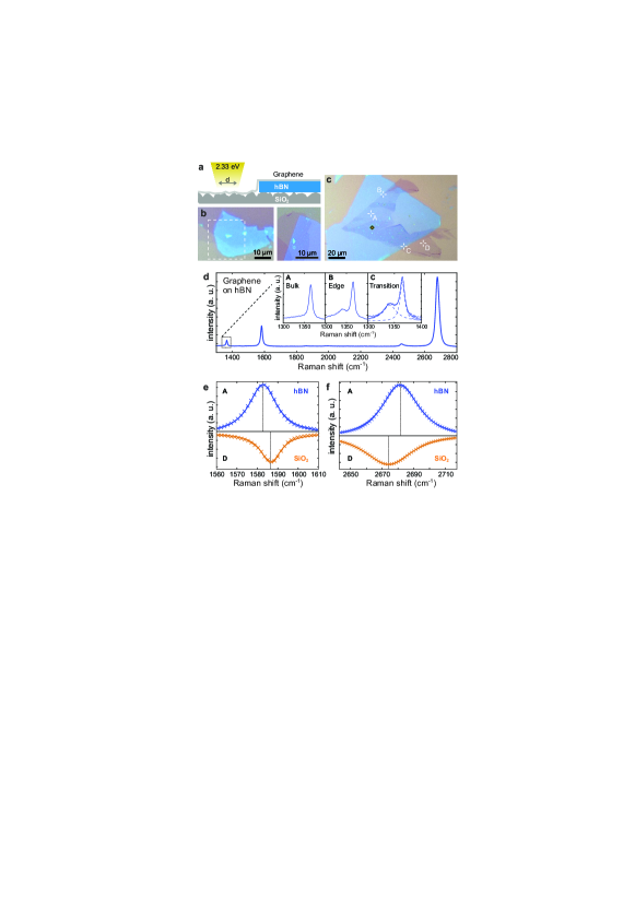
Graphene and hBN flakes are prepared by micromechanical cleavage. While hBN is directly deposited on a SiO2/Si++ substrate, graphene is prepared on top of a polymer stack consisting of a water-soluble polymer [100 nm Polyvinylalcohol (PVA)] and a water resistant polymer [270 nm Polymethyl methacrylate (PMMA)] allowing the transfer process described in detail in Ref. 8. Before depositing the graphitic flakes on top of the hBN, Raman spectroscopy has been used to identify and select individual single-layer graphene flakes fer06 ; dav07a . The Raman data are recorded by using a laser excitation of 532 nm (=2.33 eV) through a single-mode optical fiber whose spot size is limited by diffraction. A long working distance focusing lens with numerical aperture of 0.85 is used to obtain a spot size of approximately 400 nm. We used a laser power below 1 mW such that heating effects can be neglected jun07a .
II.2 Raman spectroscopy measurements
A schematic illustration of our structures is shown in Fig. 1a and optical microscope images of some fabricated samples are shown in Figs. 1b-c. A typical Raman spectrum of a graphene flake resting on hBN is shown in Fig. 1d. The Raman spectrum shows the prominent G-line around 1582 cm-1 as well as the single Lorentzian shaped 2D-line around 2675 cm-1 as expected for graphene. A third prominent and sharp peak arises around 1365 cm-1, which can be attributed to the Raman active LO-phonon in hBN gei66 . It is important to distinguish this peak from the defect induced D-line potentially appearing at around 1345 cm-1 dav07a . Therefore, Raman spectra have been acquired at edge regions of the graphene flake where defects are known to appear dav07a . The insets in Fig. 1d show corresponding Raman spectra at different positions marked and labeled in Fig. 1c. The data recorded at the edge (B) shows a second peak arising at around 1345 cm-1 which is not visible in the bulk region and can be clearly distinguished from the one at 1365 cm-1. As shown in inset C of Fig. 1d, the D-line also appears in regions of substrate transition, i.e. at the edge of the underlying hBN flake. This can be attributed to local bending of the graphene flake induced by the level difference of the two substrates. The sp2+η hybrid orbitals necessary to bend the graphene layer cause short range scattering leading to a D peak in the Raman spectrum. The D line is not visible in regions of graphene away from the edges, neither on hBN nor on SiO2. We conclude that the transfer technique used in the fabrication process does not induce a significant amount of defects in the graphene lattice.
In order to show the substrate dependence of the Raman lines of graphene, we compare in Figs. 1e-f the G and 2D-lines of a flake that partially rests on hBN and partially on SiO2. The G peak of graphene on hBN and the one on SiO2 differ significantly in their position: the G peak on SiO2 is centered at 1586.5 cm-1 while the one on hBN is centered at 1582.8 cm-1. This downshift can be attributed to reduced doping, which also is consistent with the increase of the full width at half maximum (FWHM) of the G peak of graphene on hBN yan07 . The FWHM is 12.2 cm-1 on SiO2 and 16.7 cm-1 on hBN. Also the 2D peak shows a substrate dependence of the position which is 2674.0 cm-1 on SiO2 and 2681.6 cm-1 on hBN. The substrate dependence of the 2D FWHM is even more significant, being 36.4 cm-1 on SiO2 and 28.1 cm-1 on hBN.
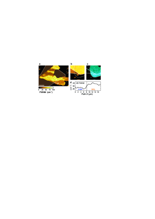
The peak-shifts and changes in the FWHM can not only be seen in individual Raman spectra, but also appear spatially resolved in two dimensional Raman maps. A Raman map of the 2D FWHM of the sample presented in Fig. 1c is shown in Fig. 2a. One can identify three single layer regions with a FWHM below 40 cm-1, two resting on hBN and one resting on SiO2 with a small region also resting on hBN. A line cut in this substrate transition region shown in Fig. 2d reveals a locally resolved difference of the FWHM of around 8 cm-1. Fig. 2b shows the 2D FWHM map of the sample previously shown in Fig. 1b (left panel). There is also a substrate dependency visible. A Raman map of the integrated peak intensity between 1360 and 1370 cm-1 is shown in Fig. 2c. The bright area has exactly the same shape as the underlying hBN flake in the optical picture and verifies the attribution of this peak to the hBN mode.
II.3 Statistical analysis
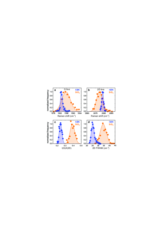
To relate the quantitative results of the measurements to physical properties like charge carrier density fluctuations and to dispose of statistical fluctuations, it is necessary to evaluate a large number of spectra statistically. The statistical distribution of the G peak position of the flake of Fig. 1c, only considering single-layer regions, is plotted in Fig. 3a. These data show a clear distinction between the different substrates. To obtain estimates of the statistical parameters the distribution is considered to be approximately Gaussian. The mean value of the distribution on hBN, =1583.1 cm-1, is red shifted with respect to the one on SiO2, =1585.9 cm-1, a notable deviation by almost three wavenumbers. Even more pronounced is the difference in the standard deviation which is a measure for the G peak fluctuations. Being =0.7 cm-1 on hBN, it is almost four times smaller than on SiO2 where =2.7 cm-1.
Previous Raman measurements with gated graphene flakes on SiO2 have demonstrated a dependency of the G peak position on the charge carrier density das08 ; sta07 . A non-adiabatic theory was established to calculate the G-peak shift in terms of charge carrier densities laz06 ; pis07 . By using a finite temperature of 295 K and an intrinsic G peak position of 1582.5 cm-1 according to das08 , we obtain a charge carrier density of 1.8 cm-2 on SiO2 and 9 cm-2 on hBN, meaning the overall doping of the investigated single-layer flake on hBN is reduced by a factor of two with respect to a region of the very same flake resting on SiO2. Please note that the doping induced G-peak shifts are well consistent with the observed FWHMs of the corresponding G-lines sta07 ; yan07 .
Furthermore, using the standard deviation of the G-peak-shift distribution to quantify the charge fluctuations, one obtains a fluctuation of 1.6 cm-2 on SiO2 and a fluctuation of 6 cm-2 on hBN. This difference by almost a factor of three indicates a significant reduction in doping domain fluctuations and hence a reduction of the disorder potential in the single-layer graphene on hBN. Comparing these results with the data obtained by scanning tunneling spectroscopy xue11 ; dec11 , one will notice a difference by one to two orders of magnitude. However, the experiments using scanning tunneling spectroscopy, besides being carried out in a low temperature controlled environment, acquire data with an atomic resolution from an area of 100 nm2 which is on the scale of individual charge puddles, the Raman setup with a spatial resolution of around 500 nm is capable of measuring on a micrometer scale averaging over a large number of charge puddles. For instance, the areas used to acquire the data on this sample are around 50 m2 on SiO2 and around 100 m2 on hBN.
As shown in previous works, the reduced doping fluctuations are also manifested in a reduced ratio between the integrated peak intensities of the G and 2D peak das08 ; bas09 . The statistical distribution depicted in Fig. 3c shows a clear substrate dependency of this ratio and is in qualitative agreement with the G peak evaluation.
Experimental data of the statistics of the FWHM of the 2D-line is provided in Fig. 3d. The mean values for the two substrates are clearly different and also the standard deviations differ. Consistent with the two dimensional Raman map shown before, the 2D peak width of the regions on hBN (=25.2 cm-1) is significantly smaller by almost 10 cm-1 than the one on SiO2 (=34.5 cm-1). Also the fluctuations of the hBN data, =1.3 cm-1, are significantly smaller than the ones of the SiO2 data, =2.7 cm-1. So far, the FWHM of the 2D peak was not considered to be doping dependent. Measurements of gated graphene on SiO2 showed no significant dependence on the charge carrier density sta07 . Hence, a reduced doping alone cannot explain this substrate dependence. A similar reduced line-width of the 2D-line (23 cm-1) was observed for suspended graphene berciaud ; berciaud13 . We assume that the increased FWHM for graphite on SiO2 is due to the substrate roughness and the presence of impurities which gives rise to an enhanced electron scattering and thus a smaller life-time of the excited electronic states during the double-resonant Raman process.discuss
III Discussion
We now turn to the discussion of the 2D-line position whose statistical distribution on hBN and on SiO2 is shown in Fig. 3b. While the position of the G-line can be directly related to the presence or absence of residual charging due to impurities on or in the substrate, the interpretation of the 2D-line shift is more subtle. Small charge densities ( 41012 cm-2) lead to shifts of the 2D-line by at most 2 cm-1 (Ref. 5). Furthermore, the 2D-line positions of suspended graphene berciaud and graphene on hBN differ by almost 10 cm-1 even though both systems are mostly free of charge impurities, as demonstrated by the coincidence of the G-line positions. Thus, we discard charging as the origin for the 2D-line shift.
Our interpretation of the 2D-line shift is based on the double-resonance Raman model of Thomsen and Reich thomsen00 . The model successfully describes the D and 2D dispersion as a function of laser energy as well as the splitting of the 2D-line for bilayer, and few-layer graphene fer06 ; dav07a ; venezuela , provided that renormalization of the highest optical phonon branch (HOB) due to electron-correlation effects is properly taken into account lazzeri08 .
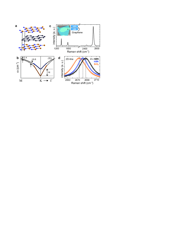
According to the double-resonance model, the 2D-line dispersion is proportional to the slope of the HOB between the high-symmetry points K and M, and inversely proportional to the slope of the bands around K. In a first step, we thus calculated the electronic band structure and the phonon-dispersion of graphene on hBN using standard density-functional theory in the local density approximation (DFT-LDA). We chose the most stable configuration where one carbon atom is on top of a boron atom and the other carbon atom in the hollow site of hBN giovannetti . In the electronic band-structure a small gap of 53 meV opens at K but further away from K, the -bands remain almost unchanged giovannetti . In the phonon dispersion, calculated by density-functional perturbation theory (DFPT) gonze , there is only a small change of the HOB in the immediate neighborhood around K. There, one observes a slight smearing of the Kohn anomaly (due to the very small band-gap opening), manifest in an up-shift of the HOB by about 3 cm-1. Everywhere else between K and M, in particular in the wave-vector range that is sampled in Raman experiments, the upshift of the HOB is less than 1 cm-1. We conclude that the pure “mechanical” interaction alone between graphene and the hBN substrate cannot explain the blue-shift of the Raman 2D-line random_note .
In recent work, it was shown by calculations on the level of the GW-approximation gwreview that electronic correlation beyond DFT-LDA influences both the slope of the -bands of graphene gruneis ; trevisanutto and the slope of the highest-optical phonon branch around K lazzeri08 . The electron-electron interaction depends on the electronic screening by the environment. Therefore, we expect that correlation effects in graphene will be reduced by a dielectric substrate. Although SiO2 and hBN have both roughly the same dielectric constant, the coupling between graphene and ultra-flat hBN is significantly increased compared to graphene on rough SiO2 (see also illustration in Fig. 1a). This different dielectric environment will have consequences for the Fermi velocity and for the electron-phonon coupling. In order to verify this hypothesis, we have performed GW-calculations on isolated (suspended) graphene and on graphene surrounded by two layers of hBN. The periodic geometry that we used in our calculations is shown in Fig. 4a. For simplicity, we have symmetrized the unit cell by choosing an ABC stacking sequence for the three layers. This ensures that the two carbon atoms in the unit-cell are equivalent, each with a boron atom on one side and a hollow site on the other side. Due to the symmetry, the linear crossing of the -bands is preserved and we can use the same strategy as in Ref. 31 for the calculation of the electron-phonon coupling at the high-symmetry point K: In the supercell, the atoms are displaced by a small distance ( atomic units) from their equilibrium position along the eigenvector of the HOB (see Fig. 3b of Ref. 31). The squared electron-phonon (e-ph) coupling – which determines the slope of the HOB around K piscanec – is then obtained as
| (1) |
where is the induced energy gap between the and bands at K.
|
|
||||||
|---|---|---|---|---|---|---|---|
| (eV) | LDA | 0.1414 | 0.1388 | ||||
| GW | 0.2158 | 0.2070 | |||||
| (eV2/Å2) | LDA | 89.25 | 86.00 | ||||
| GW | 207.88 | 191.27 | |||||
In Table 1, we present the results of our calculations (see Appendix for details). On the LDA level, the e-ph coupling is 3.7% weaker for graphene surrounded by hBN than for pure (suspended) graphene. This difference is increased to 8% on the level of the GW approximation. Obviously, the increased screening by the hBN substrate reduces the gap opening and thus the e-ph coupling note_gap_opening . Since the slope of the HOB around K is proportional to the e-ph coupling piscanec and since the frequency of the HOB far away from K is almost independent of screening effects lazzeri08 , a reduction of the e-ph coupling leads to an increase of the HOB frequency at and around K. This is demonstrated in Fig. 4b. In order to quantitatively understand this effect, it would be desirable to calculate the exact phonon dispersion relation including correlation effects. Due to the complexity of total-energy GW calculations, this is currently not feasible. A workaround consists in the use of the hybrid B3LYP functional b3lyp where we adjust the parameters in order to mimic the two different screening values for “pure” and “sandwiched” graphene (see details in the Appendix). Using these functionals, we obtain that the HOB shifts (from “pure” to “sandwiched” graphene) by +16 cm-1 at K, by +2.4 cm-1 at M, and by +6.8 cm-1 half-way between K and M (which corresponds to a excitation energy of 2.8 eV). At the same time, the frequency at remains almost unchanged (-0.4 cm-1). For the laser energy of 2.33 eV, linear interpolation yields a phonon shift of +8.3 cm-1. The corresponding 2D-line shift (where 2 phonons are excited/absorbed) would be then +16.6 cm-1. These calculations are not meant to provide absolute numbers for the 2D-line shift but they demonstrate that the experimentally measured 2D-line shift qualitatively agrees with the shift that is induced by the enhanced dielectric screening for graphene on hBN note_GWbands .
So far, we have compared a calculation for graphene surrounded by hBN with experiments where graphene is deposited on top of a hBN flake. This motivated us to perform Raman measurements on graphene surrounded by hBN on both sides. We achieved this by the deposition of an additional multi-layer hBN flake on top of one of our graphene on hBN samples. The resulting Raman spectrum is shown in Fig. 4c. The spectrum displays three prominent peaks: the peak at 1367 cm-1 is the E2g2-mode of hBN. The G-line of graphene at 1583.7 cm-1 is approximately in the same position as the G-line of graphene with hBN on one side. This evidences that only a few additional charge impurities are added during the deposition of the top-hBN flake. In contrast to the G-line, the 2D-line of surrounded graphene around 2687.4 cm-1 is considerably blue-shifted by 7 cm-1 compared to the 2D-line of one-sided graphene on hBN as shown in Fig. 4d. With respect to suspended graphene (2673.5 cm-1) berciaud the blue-shift of the 2D-line of graphene on hBN roughly doubles when a second hBN-layer is added on top. This is another indication that the blue-shift has its origin in the screening dependence of the HOB between K and M.
IV Conclusion
Our Raman measurements confirm that hBN is a high-quality insulating substrate for graphene with strongly reduced impurity charging. This is evidenced by the red-shift of the G peak with respect to graphene on a standard SiO2 substrate. In contrast to the G-line, the 2D-line of graphene on hBN is blue-shifted. We have shown that this change in the frequency of the highest-optical branch is not a consequence of a direct (mechanical) interaction between graphene and its substrate. It is rather an indirect, electronic, effect mediated by the influence of the dielectric screening on the electronic structure of graphene. Usually, in three-dimensional metallic systems, the phonon-frequencies close to a Kohn anomaly depend only on the internal screening of the (bulk) material. Layered graphene is an example where (close to the Kohn anomaly at K), the frequencies of the highest optical branch depend on the external screening by the dielectric environment. This constitutes a new physical paradigm that is worthwhile to be investigated also in other layered materials. The electron-phonon coupling between the -bands and the highest optical branch around can also impose a limitation on the conductivity of graphene in the high current-limit lazzeri2006 . Therefore, the dielectric screening of electron-phonon coupling in 2-dimensional layered materials can play a general role for transport in layered materials.
Acknowledgments
Financial support by the DFG (SPP-1459 and FOR-912) and the ERC is gratefully acknowledged. A.M.-S. and L.W. acknowledge funding by the ANR (French National Research Agency) through project ANR-09-BLAN-0421-01. Calculations were done at the IDRIS supercomputing center, Orsay (Proj. No. 091827), and at the Tirant Supercomputer of the University of Valencia (group vlc44).
Appendix: Details on the calculations
The DFT calculations are performed with the code ABINIT. Wave-functions are expanded in plane-waves with an energy cutoff at 35 Ha. Core electrons are replaced by Trouiller-Martins pseudopotentials. The periodic supercell comprises two layers of hBN and one layer of graphite with 20 a. u. of vacuum distance towards the neighboring slab in order to keep the interaction between neighboring slabs small. We use the experimental in-plane lattice constant of graphite, Å, and “squeeze” the hBN layers to the same value in order to keep the calculations simple.
The inter-layer spacing between adjacent hBN-layers is 3.33 Å (experimental value of bulk hBN) and between graphene and hBN 2.46 Å (theoretical value, obtained from geometry optimization of graphene on hBN). For the calculations of “isolated” graphene, we use the same supercell, just removing the hBN-layers. The spacing between the graphene layers is thus the same in both cases. In one case, there is vacuum between the layers, in the other case, the vacuum is “filled” with hBN-layers. The Brillouin zone is sampled with a -point grid. The GW calculations have been done with the code Yambo yambo , using the plasmon-pole approximation for the dielectric constant. The convergence parameters are the same as in Ref. 31. is used in the present work. The values for the electron-phonon coupling for pure graphene in Table 1 are slightly different than in Ref. 31 due to the different spacing between the layers which leads to a difference in the (average) dielectric constant.
The B3LYP exchange-correlation energy has the following form
where is the GGA exchange potential by Becke becke , is the Hartree-Fock exchange potential, is the LDA correlation potential by Vosko, Wilk, and Nusair vosko , and is the GGA correlation potential by Lee, Yang, and Parr leeyangparr . The usual choice of the mixing parameters is . The parameter determines the admixture of Hartree-Fock exchange. Increasing leads to a stiffening of the bonds (increasing thereby all optical phonon frequencies). Increasing the parameter which determines the admixture of non-local correlation increases the bond-strength as well. We therefore change the two parameters in opposite directions in order to keep the bond-strength constant. Changing the parameter and then mimics, roughly, a change of screening. Using the code CRYSTAL crystal , we fit the parameters and such that we obtain the same values for the e-ph coupling matrix elements, as calculated on the level of the GW-approximation. For the case of isolated graphene, we obtain , for the case of surrounded graphene, we obtain . We emphasize, that this calculation is only meant to provide a rough quantitative estimate and cannot reproduce the full physics of the dielectric screening of the Kohn anomaly of the HOB.
References
- (1) M. I. Katsnelson, ”Graphene - Carbon in Two Dimensione”, Cambridge University Press, (2012).
- (2) A. H. Castro Neto, F. Guinea, N. M. R. Peres, K. S. Novoselov, and A. K. Geim, Rev. of Mod. Phys. 81, 109 (2009).
- (3) D. R. Cooper, B. D’Anjou, N. Ghattamaneni, B. Harack, M. Hilke, A. Horth, N. Majlis, M. Massicotte, L. Vandsburger, E. Whiteway, and V. Yu, ISRN Cond. Mat. Phys. 2012, 501686 (2012).
- (4) J. Martin, N. Akerman, G. Ulbricht, T. Lohmann, J. H. Smet, K. von Klitzing, and A. Yacoby, Nat. Phys. 4, 144 (2008).
- (5) C. Stampfer, F. Molitor, D. Graf, K. Ensslin, A. Jungen, C. Hierold, and L. Wirtz, Appl. Phys. Lett. 91, 241907 (2007).
- (6) L. A. Ponomarenko, R. Yang, T. M. Mohiuddin, M. I. Katsnelson, K. S. Novoselov, S. V. Morozov, A. A. Zhukov, F. Schedin, E. W. Hill, A. K. Geim, Phys. Rev. Lett. 102, 206603 (2009).
- (7) X. Wang, J.-B. Xu, C. Wang, J. Du, and W. Xie, Adv. Mater. 23, 2464 (2011).
- (8) C. R. Dean, A. F. Young, I. Meric, C. Lee, L. Wang, S. Sorgenfrei, K. Watanabe, T. Taniguchi, P. Kim, K. L. Shepard, and J. Hone, Nat. Nanotechnol. 5, 722 (2010).
- (9) A. S. Mayorov, et al. Nano Lett. 11, 2396 (2011).
- (10) J. Xue, J. Sanchez-Yamagishi, D. Bulmash, P. Jacquod, A. Deshpande, K. Watanabe, T. Taniguchi, P. Jarillo-Herrero, and B. J. LeRoy, Nat. Mat. 10, 282 (2011).
- (11) R. Decker, Y. Wang, V. W. Brar, W. Regan, H. Tsai, Q. Wu, W. Gannett, A. Zettl, M. F. Crommie, Nano Lett. 11, 2291 (2011).
- (12) B. Arnaud, S. Lebègue, P. Rabiller, and M. Alouani, Phys. Rev. Lett. 96, 026402 (2006).
- (13) The measured (in-plane) lattice constants are = 2.4589(5) Å for graphite bas55 and = 2.504(2) Å for hexagonal boron nitride sol95 .
- (14) Y. Baskin and L. Meyer, Phys. Rev. 100, 544 (1955).
- (15) V. L. Solozhenko, G. Will, and F. Elf, Solid State Commun. 96, 1 (1995).
- (16) A. C. Ferrari, J. C. Meyer, V. Scardaci, C. Casiraghi, M. Lazzeri, F. Mauri, S. Piscanec, D. Jiang, K. S. Novoselov, S. Roth, and A. K. Geim, Phys. Rev. Lett. 97, 187401 (2006).
- (17) D. Graf, F. Molitor, K. Ensslin, C. Stampfer, A. Jungen, C. Hierold, and L. Wirtz, Nano Lett. 7, 238 (2007).
- (18) A. Gupta, G. Chen, P. Joshi, S. Tadigadapa, and P. C. Eklund, Nano Lett. 6, 2667 (2006).
- (19) S. Pisana, M. Lazzeri, C. Casiraghi, K. S. Novoselov, A. K. Geim, A. C. Ferrari, and F. Mauri, Nature Mat. 6, 198 (2007).
- (20) C. Casiraghi, A. Hartschuh, H. Qian, S. Piscanec, C. Georgi, A. Fasoli, K. S. Novoselov, A. K. Geim, and A. C. Ferrari, Nano Lett. 9, 1433 (2009).
- (21) S. Berciaud, S. Ryu, L. E. Brus, and T. F. Heinz, Nano Lett. 9, 346 (2009).
- (22) D. Bischoff, J. Güttinger, S. Dröscher, T. Ihn, K. Ensslin, and C. Stampfer, J. Appl. Phys. 109, 073710 (2011).
- (23) Q. H. Wang, Z. Jin, K. K. Kim, A. J. Hilmer, G. L. C. Paulus, C.-J. Shih, M.-H. Ham, J. D. Sanchez-Yamagishi, K. Watanabe, T. Taniguchi, J. Kong, P. Jarillo-Herrero, and Michael S. Strano, Nat. Chem. 4, 724 (2012).
- (24) L. Wang, Z. Chen, C.R. Dean, T. Taniguchi, K. Watanabe, L.E. Brus, and J. Hone, ACS Nano 6, 9314 (2012).
- (25) W. Kohn, Image of the Fermi Surface in the Vibration Spectrum of a Metal Phys. Rev. Lett. 2, 393 (1959).
- (26) S. Piscanec, M. Lazzeri, F. Mauri, A. C. Ferrari, J. Robertson. Phys. Rev. Lett. 93, 185503 (2004).
- (27) A. Jungen, V. N. Popov, C. Stampfer, L. Durrer, S. Stoll, and C. Hierold, Phys. Rev. B 75, 041405 (2007).
- (28) R. Geick, C. Perry, and G. Rupprecht, Phys. Rev. 146, 543 (1966).
- (29) J. Yan, Y. Zhang, P. Kim, and A. Pinczuk, Phys. Rev. Lett. 98, 166802 (2007).
- (30) A. Das, S. Pisana, B. Chakraborty, S. Piscanec, S. K. Saha, U. V. Waghmare, K. S. Novoselov, H. R. Krishnamurthy, A. K. Geim, A. C. Ferrari, and A. K. Sood, Nat. Nanotechnol. 3, 210 (2008).
- (31) M. Lazzeri and F. Mauri, Phys. Rev. Lett. 97, 266407 (2006).
- (32) D. M. Basko, S. Piscanec, and A. C. Ferrari, Phys. Rev. B 80, 165413 (2009).
- (33) C. Thomsen, S. Reich, Phys. Rev. Lett. 85, 5214 (2000).
- (34) P. Venezuela, M. Lazzeri, and F. Mauri, Phys. Rev. B 84, 035433 (2011).
- (35) M. Lazzeri, C. Attaccalite, L. Wirtz, and F. Mauri. Phys. Rev. B 78, 081406(R) (2008).
- (36) X. Gonze, J.-M. Beuken, R. Caracas, F. Detraux, M. Fuchs, G.-M. Rignanese, L. Sindic, M. Verstraete, G. Zérah, F. Jollet, M. Torrent, A. Roy, M. Mikami, Ph. Ghosez, J.-Y. Raty, D.C. Allan, Comp. Mat. Sci. 25, 478 (2002).
- (37) G. Giovannetti, P. A. Khomyakov, G. Brocks, P. J. Kelly, and J. van den Brink, Phys. Rev. B 76, 073103 (2007).
- (38) X. Gonze and C. Lee. Phys. Rev. B 55, 10355 (1997). S. Baroni, S. de Gironcoli, A. Dal Corso, and P. Giannozzi. Rev. Mod. Phys. 73, 515 (2001).
- (39) Note, that in the experiment, the carbon flake is deposited on top of hBN in random orientation. In this case, the band-gap remains closed sachs and the change in the Kohn anomaly of the HOB will be even less pronounced.
- (40) B. Sachs, T. O. Wehling, M. I. Katsnelson, and A. I. Lichtenstein, Phys. Rev. B 84, 195414 (2011).
- (41) For a review, see, e.g., W. G. Aulbur, L. Jönsson, and J. W. Wilkins, Solid State Physics 54, 1 (1999).
- (42) A. Grüneis, C. Attaccalite, T. Pichler, V. Zabolotnyy, H. Shiozawa, S. L. Molodtsov, D. Inosov, A. Koitzsch, M. Knupfer, J. Schiessling, R. Follath, R. Weber, P. Rudolf, L. Wirtz, and A. Rubio, Phys. Rev. Lett. 100, 037601 (2008).
- (43) P. E. Trevisanutto, C. Giorgetti, L. Reining, M. Ladisa, and V. Olevano, Phys. Rev. Lett. 101, 226405 (2008).
- (44) A. Marini, C. Hogan, M. Gruning, and D. Varsano, Comp. Phys. Comm. 180, 1392 (2009), http://www.yambocode.org.
- (45) Our GW-calculations are in line with the recent finding that the quasi-particle band-gap of “graphone” (partially hydrogenated graphene) is reduced by a hBN (or other dielectric) substrate Kharche and also with recent calculations of the band-gap of MoS2 in the presence of dielectric layers komsa .
- (46) N. Kharche and S. K. Nayak, Nano Lett. 11, 5274 (2011).
- (47) H.-P. Komsa and A. V. Krasheninnikov, Phys. Rev. B 86, 241201 (2012).
- (48) A. D. Becke, J. Chem. Phys. 98, 5648 (1993).
- (49) A. D. Becke, Phys. Rev. A 38, 3098 (1988).
- (50) S. H. Vosko, L. Wilk, and M. Nusair, Can. J. Phys. 58, 1200 (1980).
- (51) C. Lee, W. Yang, and R. G. Parr, Phys. Rev. B 37, 785 (1988).
- (52) R. Dovesi, V. R. Saunders, C. Roetti, R. Orlando, C. M. Zicovich-Wilson, F. Pascale, B. Civalleri, K. Doll, N. M. Harrison, I. J. Bush, P. D’Arco, and M. Llunell, CRYSTAL06 User’s Manual (University of Torino, Torino, 2006).
- (53) Due to the dielectric screening, the electron-electron (e-e) interaction in “sandwiched” graphene is slightly reduced and thus the Fermi-velocity slightly decreases. According to the double-resonance model, a reduction of the slope of the bands leads to a shift of the phonon-wave vector away from K towards M and thus to a blue-shift of the Raman 2D line. However, if one takes into account the effects of e-e interaction for the quasi-particle band structure, one should also take into account excitonic effects during the optical excitation of electron-hole (e-h) pairs. The increased dielectric screening, which reduces the e-e interaction, also reduces the e-h interaction. Thus the two effects tend to cancel each other and we assume that the Fermi-velocity reduction has a negligible influence on the Raman 2D-line position.
- (54) M. Lazzeri and F. Mauri, Phys. Rev. B 73, 165419 (2006).
- (55) S. Berciaud, X. Li, H. Htoon, L. E. Brus, S. K. Doorn, and T. F. Heinz, arXiv:1305.7025 [cond-mat.mes-hall] (Nano Letters, Article ASAP, (2013)).
- (56) D. M. Basko, Phys. Rev. B 78, 125418 (2008).
- (57) A detailed discussion of the 2D-line width is beyond the scope of this work. For a discussion of line-width and line-shape, we refer the reader to the work of Berciaud et al.berciaud13 on suspended graphene. The theoretical basis can be found in Ref. basko2008,