Interlayer tunneling spectroscopy of graphite at high magnetic field oriented parallel to the layers
Abstract
Interlayer tunneling in graphite mesa-type structures is studied at a strong in-plane magnetic field up to 55 T and low temperature K. The tunneling spectrum vs. has a pronounced peak at a finite voltage . The peak position increases linearly with . To explain the experiment, we develop a theoretical model of graphite in the crossed electric and magnetic fields. When the fields satisfy the resonant condition , where is the velocity of the two-dimensional Dirac electrons in graphene, the wave functions delocalize and give rise to the peak in the tunneling spectrum observed in the experiment.
1 Introduction
Over the last decade, interlayer tunneling spectroscopy was developed to measure energy gaps in high-temperature superconductors and charge-density-wave materials ref1 ; ref2 . It was also used to study magnetic-field-induced charge-density waves in NbSe3 ref3 and graphite ref4 . This latter effect has orbital origin and generally exists for a magnetic field oriented perpendicularly to the conducting layers. In contrast, the interlayer tunneling in a parallel magnetic field can be utilized to obtain information about the in-plane energy spectrum of the carriers in the layers ref5 . Tunneling experiments between two graphene sheets in the graphene/insulator/graphene heterostructure were reported in ref6 . The effect of the in-plane magnetic field was studied theoretically for graphene multilayers ref7 and for a thin film of a topological insulator theoretically ref7b ; ref8 and experimentally ref8b . Here we present an experimental and theoretical study of graphite in strong in-plane magnetic and out-of-plane electric fields.
2 Experimental Results
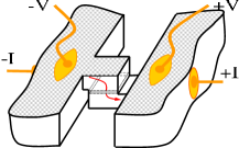
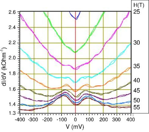

Mesa-type structures were fabricated by double-sided etching of thin graphite flakes using focused ion beam ref9 . We used high-quality natural graphite of NGS Naturgraphit GmbH Co. The mesa is shown schematically in Fig. 1. Electric current flows from one part of the crystal into another across the layers in the region of the mesa. The mesa is typically of 1 micron size and contains a few tens of graphene layers. Because of a very high interlayer conductivity anisotropy ( at low temperatures), the applied voltage drops mostly on the mesa. The experiment was performed in pulsed magnetic fields at the National Laboratory for High Magnetic Fields in Toulouse. We developed a system of fast data acquisition, which allowed us to collect about - characteristics, each containing points within each magnetic field pulse of ms duration ref3 . Figure 2 shows a set of spectra vs. for various in-plane magnetic fields. For magnetic fields greater than T, local maxima start to develop for both polarities of the bias voltage symmetrically. Both the height and the voltage of the peaks grow with the magnetic field . Figure 3 shows that the dependence of vs. is close to linear.
3 Theoretical Discussion
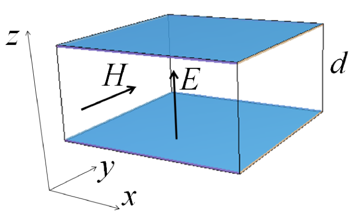
In this section, we consider a model of graphite in crossed electric and magnetic fields in the geometry shown in Fig. 4. The magnetic field is parallel to the layers, while the electric field is perpendicular, and the distance between the layers is . We shall demonstrate that, when the resonance condition for the fields
| (1) |
is achieved, the electronic wave functions become delocalized in the direction and give rise to a peak in the interlayer differential conductance, as observed experimentally in Figs. 2 and 3. The parameter m/s in Eq. (1) is the velocity of the two-dimensional Dirac electrons in graphene.
The Lorentz force from the in-plane magnetic field , acting during interlayer electron tunneling, shifts the in-plane momentum of the electrons on the -th graphene layer to , where ref7 ; ref8 . The uniform out-of-plane electric field changes the potential energy on the -th layer by , where . Thus, using the approach of Ref. ref7 , the Schrödinger equation for graphite in the crossed electric and magnetic fields can be written as
| (2) |
Here, the Pauli matrix acts on the spinor wave function , which has components on the A and B sublattices of the -th graphene layer. The matrix and the amplitude eV describe the interlayer coupling between the carbon atoms, which lie on top of each other in the Bernal-stacked graphite lattice. For simplicity, we set the in-plane momentum component below; however all calculations can be easily generalized for . In the limit of zero interlayer coupling , the energy spectrum is given by a series of Dirac cones
| (3) |
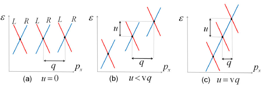
which correspond to the wave functions localized on -th graphene layer. Evolution of the spectrum (3) with the increase of the electric field is qualitatively illustrated in Fig. 5. Each Dirac cone consists of two branches corresponding to the left-moving and right-moving electrons, referred to as the L-movers and R-movers in the rest of the paper and labeled in Fig. 5(a). For , the Dirac cones are shifted horizontally by , as shown in Fig. 5(a). For , the Dirac cones are also shifted vertically, as shown in Fig. 5(b). When the fields and satisfy the resonant condition , which is equivalent to Eq. (1), the right-moving branches of the spectra align and become degenerate, as shown in Fig. 5(c).
For a more detailed analysis, let us perform a unitary transformation to the basis of the L and R movers, . Then, Eq. (2) becomes
| (4) |
If we temporary neglect the matrix , then Eq. (4) decouples for the R and L modes:
| (5) | |||
| (6) |
Solutions of Eqs. (5) and (6) can be enumerated by an integer ref7 , so that the eigenvalues are given by Eq. (3), and the eigenfunctions are
| (7) |
where is the Bessel function. The spectrum (3) is given by the two sets of curves and , which have linear dispersion in . Thus, a combination of the electric and Lorentz forces shifts the linear dispersion by for the R-movers and by for the L-movers. This results not only in different spacings between the and modes in Eq. (3), but also in different localization properties of the corresponding wave functions. The wave functions (7) are localized in the direction on a finite number of layers of the order of . So, with an increase of the electric field, the L (R) movers become more (less) localized. At the resonance condition , the R-movers experience zero net force, so their wave functions become delocalized, and the spectrum acquires a tight-binding dispersion
| (8) |
where the out-of-plane momentum is a good quantum number.
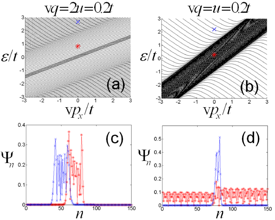
The numerically calculated energy spectra of the full Eq. (4) are shown in Fig. 6(a) and (b), whereas the corresponding wave functions are shown in Fig. 6(c) and (d). Although details of the spectra differ from the simple description given in Eq. (3), the general structure remains similar. For the case and , which was studied in Ref. ref7 , the spectrum consists of the discrete Landau levels within the energy window and a quasi-continuous spectrum outside this window . When a finite but non-resonant electric field is applied, the discrete Landau levels acquire dispersion in , as shown in Fig. 6(a). The quasi-continuous spectrum consists of a series of parallel lines corresponding to the L and R modes, well described by Eq. (3). The wave functions are localized in the direction both for the discrete Landau levels and the quasi-continuous spectrum, as shown in Fig. 6(c). However, when the resonance between the fields is achieved at , the spectrum changes drastically, as shown in Fig. 6(b). A continuous band of the R-movers corresponding to spectrum (8) emerges, and the eigenstates become delocalized, as shown in Fig. 6(d). At the same time, the L-movers remain well-localized.
We believe that the mechanism of resonant delocalization of the wave functions in the crossed electric and magnetic fields, as discussed above, is responsible for the peaks in the differential conductance observed in the experiment. According to Eq. (1), the position of the conductance peak is proportional to the magnetic field
| (9) |
where is the effective length over which the applied voltage drops. Equation (9) is consistent with the experimental Fig. 3, from which we obtain nm, about three times longer than the interlayer spacing in graphite. This result indicates that decoupling of the interlayer Bernal correlation probably occurs in two or three intrinsic tunnel junctions. In NbSe3 mesas, it was demonstrated that the charge-density-wave decoupling can occur within two intrinsic tunnel junctions of the mesa ref9 . Although our theoretical model was developed for a large number of graphene layers, the resonant condition (1) is expected to be valid even for a few layers.
4 Conclusion
The interlayer tunneling spectra measured in graphite mesas subjected to a strong in-plane magnetic field demonstrate a peak at the voltage , which is proportional . The experimental result is consistent with the presented theory, where the wave functions of the 2D Dirac electrons in graphene layers delocalize in the out-of-plane direction when the resonant condition between the fields is achieved.
Acknowledgements.
The work was supported by RFBR grants No 11-02-01379-a, No 11-02-90515-Ukr_f_a, 11-02-12167-ofi-m, programs of RAS, by European Commission from the 7th framework program “Transnational access”, contract No 228043 “Euromagnet II” Integrated Activities, and partially performed in the frame of the CNRS-RAS Associated International Laboratory between Institut Neel and IRE “Physical properties of coherent electronic states in condensed matter”.References
- (1) V. M. Krasnov, A. E. Kovalev, A. Yurgens, and D. Winkler, Phys. Rev. Lett. 86, 2657 (2001)
- (2) Yu. I. Latyshev, P. Monceau, S. Brazovskii, A. P. Orlov, and T. Fournier, Phys. Rev. Lett. 95, 266402 (2005)
- (3) A. P. Orlov, Yu. I. Latyshev, D. Vignolles, P. Monceau, JETP Lett. 87, 433 (2008)
- (4) Yu. I. Latyshev, A. P. Orlov, D. Vignolles, W. Escoffier, P. Monceau, Physica B, 407, 1885 (2012)
- (5) S. K. Lyo, E. Bielejec, J. A. Seamons, J. L. Reno, M. P. Lilly, Yun-pil Shim, Physica E, 34, 425 (2006)
- (6) L. Britnell et al., Nano Lett. 12, 1707 (2012)
- (7) S. S. Pershoguba and V. M. Yakovenko, Phys. Rev. B 82, 205408 (2010)
- (8) A. A. Zyuzin, M. D. Hook, and A. A. Burkov, Phys. Rev. B 83, 245428 (2011).
- (9) S. S. Pershoguba and V. M. Yakovenko, Phys. Rev. B 86, 165404 (2012)
- (10) H. B. Zhang, H. L. Yu, D. H. Bao, S. W. Li, C. X. Wang, G. W. Yang, Adv. Mater. 24, 132 (2012)
- (11) A. P. Orlov, Yu. I. Latyshev, A. M. Smolovich, P. Monceau, JETP Letters, 84, 89 (2006)