Energy loss rates of hot Dirac fermions in epitaxial, exfoliated and CVD graphene
Abstract
Energy loss rates for hot carriers in graphene have been measured using graphene produced by epitaxial growth on SiC, exfoliation and chemical vapour deposition (CVD). It is shown that the temperature dependence of the energy loss rates measured with high-field damped Shubnikov-de Haas oscillations, and the temperature dependence of the weak localization peak close to zero field correlate well, with the high-field measurements understating the energy loss rates by 40% compared to the low-field results. The energy loss rates for all graphene samples follow a universal scaling of at low temperatures and depend weakly on carrier density n evidence for enhancement of the energy loss rate due to disorder in CVD samples.
pacs:
73.43.Qt, 72.80.Vp, 72.10.DiI Introduction
Despite its remarkable properties, a key problem in the commercialization of graphene has been that the fabrication method used for its discovery, micromechanical exfoliationNovoselov et al. (2004), is not amenable to large-scale commercial production. There are, however, other production methods which can easily be scaled up, such as epitaxial growth on SiC, or chemical vapour deposition (CVD) on thin metal filmsvan Noorden (2012). While both these techniques are well established, the majority of graphene research is still carried out on exfoliated graphene. The principal reasons for this are the comparative ease of graphene fabrication using this method, and that to date it still produces the highest quality samplesBolotin et al. (2008). There is therefore a great need for comparisons to be made between graphene produced by the ‘research’ method, and those produced in a more commercially amenable manner.
Carrier energy loss rates are a particularly important parameter as they influence thermal dissipation and heat management in modern electronics as well as low-temperature applications such as quantum resistance metrologyTzalenchuk et al. (2010) and hot-electron bolometersYan et al. (2012). Energy loss rates have previously been measured in exfoliated grapheneBaker et al. (2012a); Tan et al. (2011); Betz et al. (2012), with conflicting results. There has also been theoretical disagreement as to how Dirac fermions in graphene lose energy to the lattice and how this varies with temperature and carrier densityKubakaddi (2009); Tse and Das Sarma (2009). Here we compare the temperature dependence of the carrier energy loss rates in graphene produced by three different fabrication methods: exfoliation, CVD and epitaxial growth on SiC, for carrier densities ranging from 1 x 1011 cm-2 to 1.6 x 1013 cm-2 using two independent methods (weak localization (WL) and Shubnikov-de Haas (SdH) oscillations) and demonstrate that a single consistent picture exists.
II Methodology
II.1 Samples
The CVD graphene was grown on thin-film copper, subsequently transferred to Si/SiO2Chen et al. (2012). The graphene wafers were lithographed by e-beam into Hall-bars using gold-only final contacting as described in our previous work on exfoliated grapheneBaker et al. (2012a). The SiC/Graphene (SiC/G) was epitaxially grown on the Si-terminated face of SiCJanssen et al. (2011). Hall-bar devices were produced using e-beam lithography and oxygen plasma etching with large area titanium-gold contacting. UV exposure of top surface polymers was used to control the carrier density Lara-Avila et al. (2011a). The carrier mobilities as deduced from the sample resisitivity and the two dimensional carrier density were strongly carrier density dependent, falling from 24,000 cm2V-1s-1 at n = 1 x 1011 cm-2 to 6,000 cm2V-1s-1 at n = 1.6 x 1012 cm-2 for SiC/G and to 300 cm2V-1s-1 at n = 1.6 x 1013 cm-2 for the CVD graphene. All electrical measurements were carried out using DC constant-current sources and multimeters.
III Results
III.1 Shubnikov-deHaas oscillations
The conventional method of measuring the temperature dependence of the energy loss rates is by comparison of the temperature-induced damping of SdH oscillations with that induced by current heating. In both cases the damping is caused by thermal broadening of the carrier distribution. This method can be used for high density samples with a sufficient mobility to display sinusoidal oscillations. Using the well known Lifshitz-Kosevich formula, which has been shown to apply to both conventionalAndo et al. (1982) and Dirac-likeGusynin and Sharapov (2005) two dimensional systems, we calculate the carrier temperature () from the damped amplitude with
| (1) |
where is the quantum lifetime and
| (2) |
and is calculated from the separation of the N and N+1 Landau levels from
| (3) |
where B is the magnetic field and is the Fermi velocity, which is 1.1 x 10⁶ms-1 as measured in both epitaxial SiC/GMiller et al. (2009) and exfoliated material Deacon et al. (2007).
| Filling | Field | Landau | Velocity |
|---|---|---|---|
| factor | B(T) | level N | vF (ms-1) |
| 34 | 17.69 | 8 | 1.06 x 10⁶ |
| 38 | 15.83 | 9 | 1.09 x 10⁶ |
| 42 | 14.33 | 10 | 1.10 x 10⁶ |
| Average vF = | 1.083 x 10⁶ |
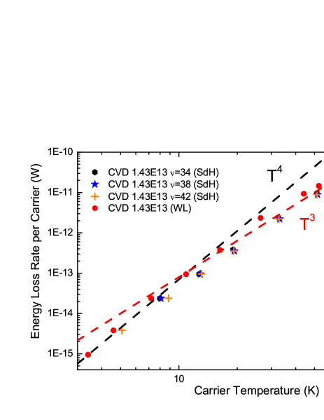
For the CVD material the carrier densities are nearly an order of magnitude higher than studied previously. To validate the method at these high carrier densities we measured the lattice temperature dependence of the damping, as shown in Fig. 2, using a sufficiently low current to avoid heating the carriers above the lattice temperature. Fig. 3 shows these amplitudes as a function of temperature fitted using Eq.1. The data are well fitted by this equation, and the Fermi velocity, vF, is deduced from Eq. 3. The measured values of vF are shown in Table 1 for a carrier density of 1.43 x 1013 cm-2. The mean value of vF = 1.083 x 10⁶ 0.02 x 10⁶ ms-1 is consistent with the values reported for exfoliated and epitaxial graphene at lower densities which shows that the Fermi velocity remains essentially constant up to energies of at least EF = 480meV.
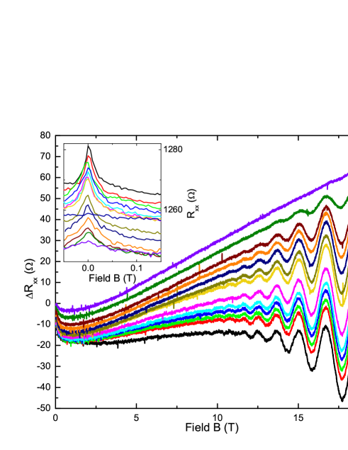
When the ambient temperature is fixed, but a current is passed through the sample, the carriers are unable to lose energy at a sufficient rate to reach thermal equilibrium with the lattice and thus heat upLeadley et al. (1989); Leturcq et al. (2003); Fletcher et al. (1992); Gershenson et al. (2000); Stöger et al. (1994). The energy loss rates were determined as a function of carrier temperature by measuring the amplitudes of the SdH oscillations as a function of current (Fig.4). Comparing the amplitudes to the undamped value, taken at low current, and using Eq.(1), the carrier temperature for each trace is determined. The associated energy loss rate per carrier (P) is calculated using
| (4) |
where is the longitudinal sample resistance, n is the carrier density, and A is the device area between the resistivity contacts where the power is dissipated.
III.2 Weak Localization
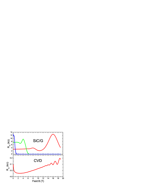
For some samples, however, the SdH method for extracting energy loss rates could not be applied, most notably for the lower carrier density SiC/G devices, where the carrier densities are too low to support a series of sinusoidal SdH oscillations (Fig. 1). SiC/G samples do, however, have prominent WL peaks.
The magnitude of the WL peak is knownCao et al. (2010); Lara-Avila et al. (2011b); Baker et al. (2012b) to be strongly damped by increasing temperature. Energy loss rates have previously been measured as a function of carrier temperature from WL peaks for several other materialsLeturcq et al. (2003); Fletcher et al. (1992); Gershenson et al. (2000); Stöger et al. (1994). In GaAsFletcher et al. (1992) good agreement was found between the values for electron temperature deduced from the WL peak and SdH oscillations at low fields (0.5T) up to 4K. Similarly excellent agreement was found for the two methods in SiGeLeturcq et al. (2003) but could only be studied for electron temperatures up to 1.1K. In our work the WL peak persists up to temperatures of almost 100K allowing a much more extensive range of parameters to be studied. Previous work in grapheneLee et al. (2010), however, was not able to determine energy loss rates from the damping of the WL peak.
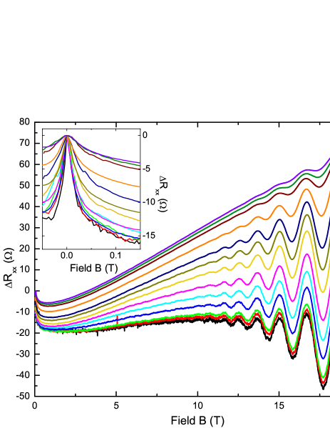
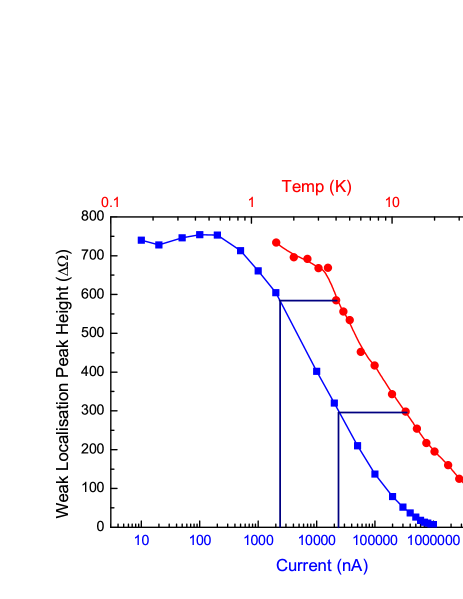
We determine the energy loss rates by comparison of the current and temperature dependence of the WL peak. The magnitudes of the peaks are measured by taking the difference of Rxx between 0T and a fixed small field, sufficient to entirely suppress the WL behavior. The temperature dependent peak height measured at low current is fitted with an interpolated curve. The magnitude of the WL peak measured as a function of current is then compared with the interpolated temperature dependence and used to deduce the carrier temperature as a function of current (Fig. 5).
It is worth emphasizing that for the above analysis to be correct, the effects of raising both the carrier and lattice temperature (TL) need to be equivalent. For this to be the case the inelastic scattering time must only depend on the carrier temperature, and be independent of the lattice temperature. This has been verified by Ki et al.Ki et al. (2008) by measuring the effect on of changes to the carrier density at temperatures up to 20K. The inelastic scattering, , in graphene was shown to depend on Coulomb interactions and Nyquist scattering, both of which vary with carrier temperature only. This can be qualitatively seen by the similar functional dependence upon current and temperature, shown in Fig. 5.
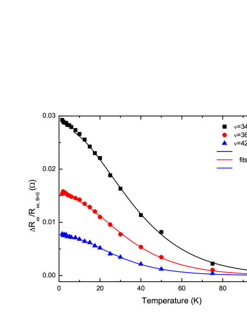
III.3 Energy Loss Rates
The temperature dependence of the energy loss rates as measured by both techniques up to 90K are shown in Fig. 6 for a CVD sample which compares the results for the WL method and analysis using the SdH method at three different occupancies. This demonstrates that there is a power law dependence of the energy loss rates which tends towards T4 at low temperature and that there is also a systematic difference between the two methods with the SdH technique giving energy loss rates 40% lower (Table 2) at any given electron temperature. This difference is in contrast to GaAsFletcher et al. (1992) and SiGeLeturcq et al. (2003) where good agreement between the two methods was found when SdH oscillations below 1T were analysed. We attribute this to a magnetic-field suppression of the energy loss rate, as the WL method measures the energy loss rate near 0T, whereas the relatively low mobilities in most graphene samples require the SdH method to make measurements at much higher fields, typically 10T to 18T in our samples, where the Landau quantization energy is 30 to 50 meV and significant changes in the current distribution also occur. No systematic dependence of electron temperature as a function of occupancy factor, , could however, be detected at high fields, as shown in Fig. 6 for =34, 38 and 42. Taken altogether therefore, these methods allow the systematic measurement of the energy loss rates per carrier as a function of carrier temperature for any graphene sample, and permit a robust comparison to be made between such samples.
| Sample Type | Carrier Density | SdH | WL | SdH / |
|---|---|---|---|---|
| (cm-2) | (W K-4/ | (W K-4/ | WL | |
| carrier) | carrier) | |||
| CVD | 2.4 | 3.8 | 0.63 | |
| CVD | 2.0 | 3.0 | 0.67 | |
| CVD | 2.2 | 3.7 | 0.59 | |
| Epitaxial | 2.1 | 3.7 | 0.57 | |
| Average = | 0.62 |
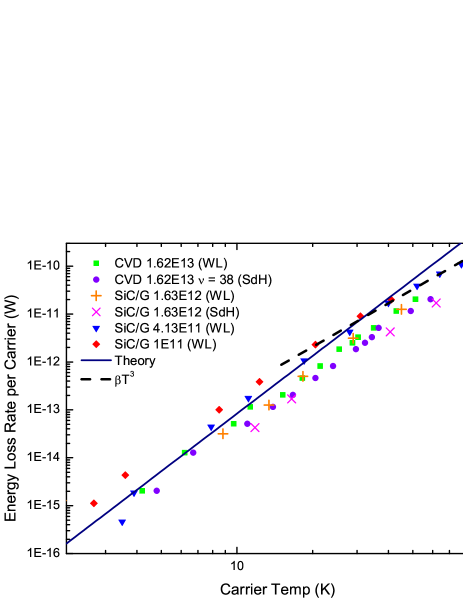
Fig. 7 summarises the results from both techniques on all of the types of graphene, with the exception that only the SdH method could be used on the exfoliated graphene, which does not exhibit large WL peaksMorozov et al. (2006). Overall this demonstrates that there are no significant differences in the systematic behaviour between samples derived from the different production methods. We find that samples produced by all the measured production methods are well fitted to a low temperature, limiting behaviour of , where is a scaling constant that is weakly carrier density dependent. This can be approximated to the form when TL Te. Theoretical predictions of the energy loss rate at low temperatures from KubakaddiKubakaddi (2009) are shown for the example of a carrier density of n = 4.13 x 1011 cm-2. These are dominated by deformation potential coupling and are shown to be an excellent fit with a deformation potential of 19 eV. This power law behaviour is typical for low temperatures below the Bloch-Grüneisen temperature () as observed for the resistivity in grapheneEfetov and Kim (2010) and is broadly consistent with the results of Betz et al.Betz et al. (2012) who reported an approximate power law at high electron temperatures, but with a reduced coupling constant. This is in contrast to some previous theoreticalTse and Das Sarma (2009) and experimentalTan et al. (2011) work which suggested other powers of T.
The value of (=, where is the Fermi wavevector) for the samples studied is in the range 10-125K (1-160 x 1011 cm-2), but as found previously in GaAsLeadley et al. (1989) the data show no evidence of approaching a high temperature limit of linear T dependence, even at temperatures significantly above . At the highest temperatures there is however some decrease in the energy loss rate, closer to a power law in the region of or lower, as reported previously for exfoliated grapheneBaker et al. (2012a) at high . It is likely that at higher temperatures above 100K some additional contribution may occur due to optical phonons in both the graphene and the substrateTse and Das Sarma (2009)Chen et al. (2008).
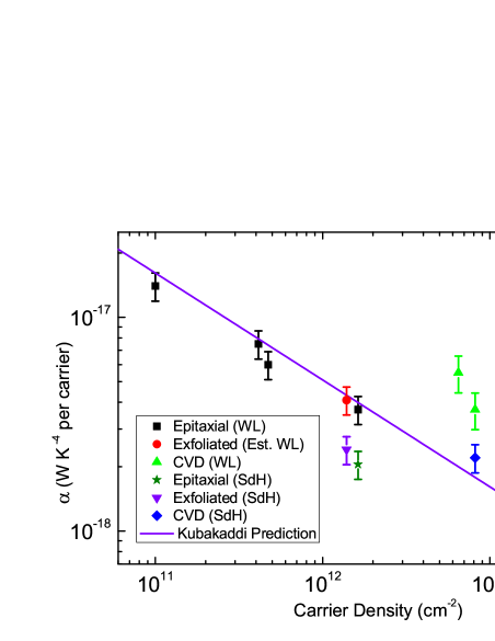
Fig. 8 shows the fitted coefficient for data below 30K for all the measured samples, and where possible for multiple measurement techniques, plotted against carrier density. The theoretical predictionsKubakaddi (2009) of the absolute values are in excellent agreement with experiment for the epitaxial and exfoliated samples and show an dependence on carrier density as predicted. However for CVD samples the energy loss rates appear to be a factor of 2 - 3 larger. Recent theoretical work from Song et al.Song et al. (2012) has proposed enhanced energy loss processes in graphene which they term “supercollisions”. These are caused by disorder-assisted, and two-phonon scattering at high k values and are particularly important for higher energy carriers which play a disproportionately large role in the energy loss processes. Our CVD samples contain significant amounts of disorder and hence the “supercollision” process could potentially account for the increased energy loss rates of the CVD samples relative to the theoretical predictionsKubakaddi (2009). Song et al. predict that for strongly disordered samples (using 2) this should give a dependence above , which has recently received experimental support from measurements of optical heatingGraham et al. (2013) and noise thermometryBetz et al. (2013). Fitting the higher temperature data for the CVD samples in Fig. 7 gives P , suggesting that this process is beginning to contribute to the energy loss rate.
IV Conclusions
In conclusion we have performed an extensive comparison of the transport properties of graphene produced by the three most common production methods. The energy loss rates per carrier as a function of carrier temperature follow a low temperature limiting T4 dependence in all cases, with a multiplicative factor that varies weakly with carrier density in good agreement with theoryKubakaddi (2009) based on deformation potential scattering. The close agreement between epitaxial graphene grown on SiC and exfoliated flakes deposited on SiO2 suggest that the substrate plays very little role in determining the energy loss rates. An enhanced energy loss rate is observed in CVD samples deposited onto SiO2 which may be attributable to “supercollisions”Song et al. (2012) allowed by the presence of increased disorder and which may be beneficial for high power electronic applications of graphene. We have also established that energy loss rates can be measured over a wide temperature range using the WL correspondence method and correlate well with the conventional SdH method, but the values deduced at high fields (10-18T) are suppressed by 40% relative to the low field values.
V Acknowledgements
This work was supported by the UK EPSRC, Swedish Research Council and Foundation for Strategic Research, UK National Measurement Office, and EU FP7 STREP ConceptGraphene.
References
- Novoselov et al. (2004) K. S. Novoselov, A. K. Geim, S. V. Morozov, D. Jiang, Y. Zhang, S. V. Dubonos, I. V. Grigorieva, and A. A. Firsov, Science 306, 666 (2004).
- van Noorden (2012) R. van Noorden, Nature 483, S32 (2012).
- Bolotin et al. (2008) K. Bolotin, K. Sikes, Z. Jiang, M. Klima, G. Fudenberg, J. Hone, P. Kim, and H. Stormer, Solid State Commun. 146, 351 (2008).
- Tzalenchuk et al. (2010) A. Tzalenchuk, S. Lara-Avila, A. Kalaboukhov, S. Paolillo, M. Syväjärvi, R. Yakimova, O. Kazakova, T. J. B. M. Janssen, V. Fal’ko, and S. Kubatkin, Nat. Nanotechnol. 5, 186 (2010), ISSN 1748-3395.
- Yan et al. (2012) J. Yan, M.-H. Kim, J. A. Elle, A. B. Sushkov, G. S. Jenkins, H. M. Milchberg, M. S. Fuhrer, and H. D. Drew, Nat. Nanotechnol. 7, 472 (2012).
- Baker et al. (2012a) A. M. R. Baker, J. A. Alexander-Webber, T. Altebaeumer, and R. J. Nicholas, Physical Review B 85, 115403 (2012a).
- Tan et al. (2011) Z. Tan, C. Tan, L. Ma, G. T. Liu, L. Lu, and C. L. Yang, Phys. Rev. B. 84, 115429 (2011).
- Betz et al. (2012) A. Betz, F. Vialla, D. Brunel, C. Voisin, M. Picher, A. Cavanna, A. Madouri, G. Feve, J.-M. Berroir, B. Placais, et al., Phys. Rev. Lett. 109, 056805 (2012).
- Kubakaddi (2009) S. S. Kubakaddi, Physical Review B 79, 075417 (2009).
- Tse and Das Sarma (2009) W.-K. Tse and S. Das Sarma, Physical Review B 79, 235406 (2009).
- Chen et al. (2012) C.-H. Chen, C.-T. Lin, Y.-H. Lee, K.-K. Liu, C.-Y. Su, W. Zhang, and L.-J. Li, Small 8, 43 (2012), ISSN 1613-6829.
- Janssen et al. (2011) T. J. B. M. Janssen, A. Tzalenchuk, R. Yakimova, S. Kubatkin, S. Lara-Avila, S. Kopylov, and V. I. Fal’ko, Phys. Rev. B. 83, 233402 (2011).
- Lara-Avila et al. (2011a) S. Lara-Avila, K. Moth-Poulsen, R. Yakimova, T. Bjø rnholm, V. Fal’ko, A. Tzalenchuk, and S. Kubatkin, Adv. Mater. 23, 878 (2011a).
- Ando et al. (1982) T. Ando, A. B. Fowler, and F. Stern, Rev. Mod. Physics 54, 437 (1982).
- Gusynin and Sharapov (2005) V. P. Gusynin and S. G. Sharapov, Phys. Rev. B. 71, 125124 (2005).
- Miller et al. (2009) D. L. Miller, K. D. Kubista, G. M. Rutter, M. Ruan, W. A. de Heer, P. N. First, and J. A. Stroscio, Science 324, 924 (2009).
- Deacon et al. (2007) R. S. Deacon, K.-C. Chuang, R. J. Nicholas, K. S. Novoselov, and A. K. Geim, Phys. Rev. B. 76, 081406 (2007), ISSN 1098-0121.
- Leadley et al. (1989) D. R. Leadley, R. J. Nicholas, J. J. Harris, and C. T. Foxon, Semicond. Sci. Technol. 4, 879 (1989).
- Leturcq et al. (2003) R. Leturcq, D. L’Hôte, R. Tourbot, V. Senz, U. Gennser, T. Ihn, K. Ensslin, G. Dehlinger, and D. Grützmacher, Europhys. Lett. 61, 499 (2003).
- Fletcher et al. (1992) R. Fletcher, J. J. Harris, C. T. Foxon, and R. Stoner, Phys. Rev. B. 45, 6659 (1992).
- Gershenson et al. (2000) M. Gershenson, Y. Khavin, D. Reuter, P. Schafmeister, and A. Wieck, Phys. Rev. Lett. 85, 1718 (2000).
- Stöger et al. (1994) G. Stöger, G. Brunthaler, G. Bauer, K. Ismail, B. S. Meyerson, J. Lutz, and F. Kuchar, Semicond. Sci. Technol. 9, 765 (1994).
- Cao et al. (2010) H. Cao, Q. Yu, L. A. Jauregui, J. Tian, W. Wu, Z. Liu, R. Jalilian, D. K. Benjamin, Z. Jiang, J. Bao, et al., Appl. Phys. Lett. 96, 122106 (2010).
- Lara-Avila et al. (2011b) S. Lara-Avila, A. Tzalenchuk, S. Kubatkin, R. Yakimova, T. J. B. M. Janssen, K. Cedergren, T. Bergsten, and V. Fal’ko, Phys. Rev. Lett. 107, 166602 (2011b).
- Baker et al. (2012b) A. M. R. Baker, J. A. Alexander-Webber, T. Altebaeumer, T. J. B. M. Janssen, A. Tzalenchuk, S. Lara-Avila, S. Kubatkin, R. Yakimova, C.-T. Lin, L.-J. Li, et al., Phys. Rev. B p. BW1789 (2012b).
- Lee et al. (2010) S. Lee, N. Wijesinghe, C. Diaz-Pinto, and H. Peng, Phys. Rev. B. 82, 045411 (2010).
- Ki et al. (2008) D. K. Ki, D. Jeong, J. H. Choi, H. J. Lee, and K. S. Park, Phys. Rev. B. 78, 125409 (2008).
- Morozov et al. (2006) S. V. Morozov, K. S. Novoselov, M. I. Katsnelson, F. Schedin, L. A. Ponomarenko, D. Jiang, and A. K. Geim, Phys. Rev. Lett. 97, 016801 (2006).
- Efetov and Kim (2010) D. K. Efetov and P. Kim, Phys. Rev. Lett. 105, 256805 (2010).
- Chen et al. (2008) J.-H. Chen, C. Jang, S. Xiao, M. Ishigami, and M. Fuhrer, Nature Nanotechnology 3, 206 (2008).
- Song et al. (2012) J. C. W. Song, M. Y. Reizer, and L. S. Levitov, Phys. Rev. Lett. 109, 106602 (2012).
- Graham et al. (2013) M. W. Graham, S.-F. Shi, D. C. Ralph, J. Park, and P. L. McEuen, Nature Physics 9, 10.1038/nphys2493 (2013).
- Betz et al. (2013) A. Betz, S. H. Jhang, E. Pallecchi, R. Ferreira, G. Feve, J.-M. Berroir, and B. Placais, Nature Physics 9, 10.1038/nphys2494 (2013).