Effects of nonlocal plasmons in gapped graphene micro-ribbon array and 2DEG on near-field electromagnetic response in the deep-subwavelength regime
Abstract
A self-consistent theory involving Maxwell equations and a density-matrix linear-response theory is solved for an electromagnetically-coupled doped graphene micro-ribbon array and a quantum-well electron gas sitting at an interface between a half-space of air and another half-space of a doped semiconductor substrate which supports a surface-plasmon mode in our system. The coupling between a spatially-modulated total electromagnetic field and the electron dynamics in a Dirac-cone of a graphene ribbon, as well as the coupling of the far-field specular and near-field higher-order diffraction modes, are included in the derived electron optical-response function. Full analytical expressions are obtained with non-locality for the optical-response functions of a two-dimensional electron gas and a graphene layer with an induced bandgap, and are employed in our numerical calculations beyond the long-wavelength limit (Drude model). Both the near-field transmissivity and reflectivity spectra, as well as their dependence on different configurations of our system and on the array period, ribbon width, graphene chemical potential of quantum-well electron gas and bandgap in graphene, are studied. Moreover, the transmitted E-field intensity distribution is calculated to demonstrate its connection to the mixing of specular and diffraction modes of the total electromagnetic field. An externally-tunable electromagnetic coupling among the surface, conventional electron-gas and massless graphene intraband plasmon excitations is discovered and explained. Furthermore, a comparison is made between the dependence of the graphene-plasmon energy on the ribbon width and chemical potential in this paper and the recent experimental observation given by Ju, et al., [Nature Nanotechnology, 6, 630 (2011)] for a graphene micro-ribbon array in the terahertz-frequency range.
I Introduction
There has been a high-level of research and device interests on both the electronic and optical properties of two-dimensional (2D) graphene material giem ; special ; ziegler1 ; orlita ; sarma1 since the report on the first successful isolation of single graphene layers as well as the related transport and Raman experiments performed for such layers first . The most distinctive difference between a graphene sheet and a conventional 2D electron gas (EG) in a semiconductor quantum well (QW) is the electronic band structure, where the energy dispersions of electrons and holes in the former are linear in momentum space but they become quadratic for the latter. As a result, electrons and holes in graphene behave like massless Dirac fermions and show a lot of unexpected physical phenomena in electron transport and optical response, including anomalous quantum Hall effect novoselov ; kim , bare and dressed state Klein tunneling novoselov1 ; kim1 ; roslyak ; iurov and plasmon excitation wunsch ; sarma ; oleksiy , a universal absorption constant mark ; nair , tunable intraband ju and interband basov ; wang optical transitions, broadband –polarization effect polar , photoexcited hot-carrier thermalization rana and transport levitov , electrically and magnetically tunable band structure for ballistic transport roslyak2 , field-enhanced mobility in a doped graphene nanoribbon huang0 and electron-energy loss in gapped graphene layers gumbs .
It has been found that most of the unusual electronic properties in graphene can be very well explained by single-particle excitation of electrons. For diffusion-limited electron transport in doped graphene, the Kubo linear-response theory kubo , as well as the Hartree-Fock theory in combination with the self-consistent Born approximation ahm , were used. Moreover, the semiclassical Boltzman theory was applied in both the linear linear and nonlinear huang0 response regimes. For the collective excitation of electrons in graphene, previous studies found it has an important role in the dynamical screening of the electron-electron interaction wunsch ; sarma ; oleksiy ; gumbs ; plasmon . However, the EM response of graphene materials has received relatively less attention, especially for low-energy intraband optical transions ju ; ziegler ; soljacic .
For any charged-particle systems, there always exists an electronic coupling based on the intrinsic electron-electron interaction in addition to the system response to an external electromagnetic field or an external electron (ion) beam. This electronic coupling can be either a classical direct coulomb interaction between any two charged particles with no requirement for an overlap of their wave functions, or quantum-mechanical tunneling and exchange coulomb interaction with a tail overlap of their wave functions book . For the same charged-particle systems, there exists another electromagnetic coupling based on the light-electron interaction huang1 . This electromagnetic coupling results from an induced optical-polarization field in the system due to dipole coupling to an incident light wave. The total electromagnetic field, including the induced optical-polarization field, should satisfy the macroscopic Maxwell equations huang2 . However, the induced optical-polarization field in the system is determined by the microscopic density-matrix equations huang3 . Therefore, a self-consistent theory is required for studying the electromagnetic response of such a charged system to incident light.
Physically, a statistical ensemble average of dipole moments in an electronic system with respect to all quantum states will give rise to an induced optical-polarization field offdiagonal . This provides a connection between the microscopic density-matrix equations and the macroscopic Maxwell equations huang3 . The former describes the full electron dynamics excited by a total electromagnetic field, including optical pumping, energy relaxation, optical coherence and its dephasing, and carrier scattering with impurities, lattice and other charged carriers scattering ; scattering1 ; scattering2 . When the incident field is weak, a self-consistent linear-response theory to the total electromagnetic field (not just the incident light) can be applied to an electronic system as a leading-order approximation.
Experimentally, the inelastic light scattering platzman and electron-energy-loss spectroscopy review were widely used for probing the bulk and surface electronic coupling, respectively, in a charged-particle system. On the other hand, the elastic light scattering aam and the optical absorption spectroscopy absorption were extensively applied for studying the surface and thin-film electromagnetic coupling in either a conductive or a dielectric system. For a smooth conductive surface, only electronic excitations in the long-wavelength limit can be coupled to an incident light wave, where a Drude-type model is usually adopted in spectroscopy analysis. For a patterned conductive surface in the deep sub-wavelength regime, on the other hand, surface light scattering can be used to explore surface electronic excitations in the system beyond the long-wavelength limit, where a wavenumber-dependent (nonlocal) optical response of electrons, which is crucial for the near-field distribution and the Landau damping of plasmons book , must be employed to analyze the light reflectivity and transmissivity spectra.
In this paper, we consider a model in which a two-dimensional electron gas (2DEG) and a doped linear graphene micro-ribbon array (electronically isolated from each other) are put on the surface of a doped semi-infinite semiconductor substrate. Therefore, we expect to see the excitations of the localized surface plasmon and the conventional 2DEG plasmon, as well as the 2D Dirac-fermion plasmon excitation, in such a system in the presence of an incident electromagnetic wave. More interestingly, we expect there to exist strong electromagnetic couplings among these three collective excitations in the deep sub-wavelength regime, i.e. with an array period much less than the incident wavelength, and these couplings can be externally tuned by the doping densities in a graphene layer or in a QW, as well as by the driven 2DEG in the QW or by the induced bandgap in the graphene. The existence of an bandgap in the graphene not only modifies the Landau damping of plasmons oleksiy , but also introduces the interplay between Dirac-like and Schrödinger-like electrons in the electromagnetic response. To demonstrate the predicted strong and tunable electromagnetic coupling among three plasmon excitations in our model system, numerical calculations and their comparisons are presented for both the transmissivity and reflectivity spectra with different configurations of our model system and various array periods, ribbon widths, chemical potentials of graphene, and induced bandgaps in graphene.
The rest of the paper is organized as follows. In Sec. II, we derive the self-consistent Maxwell equations and the density-matrix linear-response theory within the random-phase approximation for our model system which consists of a combined 2DEG in an InAs QW and a linear graphene micro-ribbon array doped by electrons on the surface of a semi-infinite -doped GaAs substrate. This self-consistent theory, along with the detailed expressions for a linear matrix equation in Appendix A, is then applied to study the transmissivity and reflectivity spectra of an incident plane wave for various structural-geometry and material parameters. In Sec. III, numerical results, including the –polarized far- and near-field transmissivity spectra as well as the transmitted –polarized E-field intensity distribution, are presented to demonstrate and explain the existence of an externally-tunable electromagnetic coupling among the localized surface plasmon, 2DEG plasmon and massless graphene plasmon excitations in our system. The conclusions drawn from these results are briefly summarized in Sec. IV.
II Model and Theory
It is shown in Fig. 1 that the half-space is air with the refractive index whereas the half-space is occupied by a doped semi-infinite GaAs substrate with a dynamical dielectric function which supports a localized surface-plasmon (SP) mode. At the interface , there are a periodic electron-doped graphene micro-ribbon array (GMRA) and an InAs quantum well (QW) for a 2DEG. Optically, the GMRA and QW can be considered to be in one plane. The reason for this is that the sheet thickness is much smaller than the wavelength and the decay length of the impinging light. They can, however, still be electrically separated from each other by an energy barrier huang1 ; huang2 . A plane-wave electromagnetic (EM) field incident from is diffracted by the GMRA into both the reflection () and transmission () regions. The diffraction modes of the EM field are modulated by the induced optical polarization at the interface with the GMRA, which will be electromagnetically coupled to SP and 2DEG plasmons.
We assume that the GMRA is periodic in the direction, and seek the solutions based on a plane-wave expansion for a single frequency. Setting for simplicity and denoting the transverse electric component of the EM field below the interface by and above by , we obtain huang1 ; huang2 ; huang3
| (4) | |||||
| (8) |
| (12) |
Here, label all reciprocal lattice vectors , is the period of the GMRA, , , , is the refractive index of air, is the angle of incidence, and the angular frequency of the incident EM field. In addition, and in Eqs. (8) and (12) are determined by the following dispersion relations for transverse EM fields
| (13) |
where is the speed of light in vacuum, is the dielectric function of the doped semiconductor substrate, and we require that so as to ensure a finite value for the reflected or transmitted EM field at .
Formally, if we keep only the term with in the summations in Eqs. (8) and (12), the GMRA in our model will simply change to a graphene sheet. For this situation, after removing the doping in the GaAs substrate and the 2DEG in the InAs QW, the formalism in this paper will reduce to the previous ones ziegler ; soljacic for a transverse EM response from a single graphene sheet.
In the long-wavelength limit, the transverse dielectric function introduced in Eq. (13) for the doped semiconductor substrate is found to be huang1 ; huang2 ; huang3
| (14) |
where is the bulk plasma frequency, is the doping concentration in GaAs, is the homogeneous level broadening, is the effective mass of electrons in the substrate and is the relative dielectric constant of the semiconductor substrate.
Once the electric field is obtained by using the Maxwell equations, the magnetic field for non-magnetic materials can be obtained from
| (15) |
where is the vacuum permeability. For and , Equation (15) explicitly leads to
| (16) |
| (17) |
| (18) |
In a similar way, the magnetic field in the region of can also be obtained from
| (19) |
| (20) |
| (21) |
Electronically, the GMRA and 2DEG can be separated by an undoped wide-gap semiconductor barrier layer. Optically, however, the GMRA and 2DEG can both be regarded as two-dimensional sheets since their thickness are much less than the EM-field wavelength considered. Therefore, the four independent boundary conditions for transverse EM fields at the interface can be written as huang1 ; huang2 ; huang3
| (22) | |||
| (23) | |||
| (24) | |||
| (25) |
where is the induced sheet optical-polarization field (related to the polarization current) while is the induced sheet conduction-current density. Furthermore, we can write as huang2 ; huang3
| (26) |
where
| (27) |
In Eq. (27), , is the width of a graphene micro-ribbon, , and and are the 2DEG and the graphene-ribbon polarizabilities, respectively. The multi-ribbon effect represented by the summation over , as well as the mode-mixing effect with , are both taken into account by the second term of Eq. (27). Moreover, the coupling between a spatially-dependent total EM field and the electron dynamics in an energy band, due to the non-locality in an optical response of electrons, is also included in Eq. (27).
| (28) |
where
| (29) |
and and are the real 2DEG and graphene-ribbon optical conductivities, respectively.
For an incoming –polarized EM field, we get and , where is the magnetic component and is the permittivity of free space.
Combining the sheet optical polarization in Eq. (26) and the sheet-current density in Eq. (28), we can write the optical-response function for in a compact form given by
| (30) |
where .
We notice that there exists an anisotropy in the polarizability of a graphene nanoribbon along the longitudinal and transverse directions ribbon , respectively, and it can be attributed to a subband quantization due to finite-size effect. However, this anisotropy can be neglected for the width of ribbons in the micrometer range. In other words, we adopt in this paper the isotropy of the micro-ribbon array instead of anisotropy of the nanoribbon array. Within the random-phase approximation, for graphene ribbons in the micrometer range we calculate the nonlocal () optical-response function as wunsch ; sarma
| (31) |
where the non-retarded limit with has been used and is defined as
| (32) |
is the surface area of a graphene micro-ribbon, is the Fermi-Dirac function for thermal-equilibrium electrons, is the kinetic energy of electrons, and represent the valence () and conduction () bands of Dirac cones in a graphene layer.
The Dirac-cone model only holds for crystal momentum that is not too large. In fact, the energy band structure ceases to be a cone above about 2.5 eV. For our medium-high-density sample used in this paper, the Fermi momentum is much less than the momentum separation between valleys at and . The Coulomb interaction between electrons in different valleys will be significantly suppressed due to this large momentum separation. Additionally, the electron-phonon mediated inter-valley scattering also requires a temperature higher than room temperature. Since we assume very low temperature for electrons in our model, this inter-valley scattering may be justifiably neglected.
The 2D dielectric function for graphene micro-ribbons can be obtained by stern in the non-retarded limit with being the dielectric constant of graphene materials. In addition, the optical conductivity of graphene ribbons can be calculated from Eq. (30) within the linear-response theory, i.e. . In a similar way, can be calculated from Eq. (51) below. Note that along with Eq. (31) correspond to 2D rather than 3D Fourier transform of the Coulomb interaction.
After a lengthy calculation oleksiy , from Eq. (32) we get an analytical expression for a gapped graphene layer at K as follows:
| (33) | |||||
where is the chemical potential of electrons in a graphene layer with respect to zero energy at , is the Fermi velocity of graphene, the kinetic energy of electrons in valence and conduction bands are
| (34) |
and is the induced bandgap. From Eq. (34) we know that a finite effective mass of electrons will be created for a gapped graphene layer close to the edge of a gap with .
The coulomb interaction between electrons will induce a self-energy, leading to an energy-dependent Fermi velocity beyond the random-phase approximation arxiv . However, this energy-dependent behavior becomes significant only around the Dirac point elias . For our samples in this paper with a very high doping concentration, we expect this effect is minimized. Therefore, we have neglected the coulomb renormalization to the graphene Fermi velocity in Eq. (34). Correction to the self-energy comes from correlation effects. However, this correction becomes significant only at low densities, as it occur, for example, when there is Wigner crystallization. However, the sample considered in this paper is of medium-high-density concentration, where correlation effects may be neglected. Since we recognize that the limitations of the model is a poor argument when it comes to the experimental data, we included in Eq. (24) an effective mass term into Dirac fermion picture. We note that the induced bandgap may be attributed to either photon dressed-state effects by circularly polarized light or to a substrate. There exist two main sources of disorder in graphene ribbons, i.e., edge roughness and charged impurities. Since wide micro-ribbons are considered in this paper, we can neglect the edge roughness. This leaves the charged impurities as the dominant scattering mechanism. The existence of charged impurities is also able to induce a self-energy, leading to a deformed density of states around the Dirac point of graphene hu . However, for our medium-high-doping samples, the screening length of impurity potential is small, leading to a negligent effect on the density of states in graphene. Moreover, with the added gap in Eq. (34), the charged impurities create localized states only in the range between and gupta . Since our transmission is not substantially affected up to eV (see Fig. 11 in Sec. III) and the induced states by localized impurities are well above the terahertz regime of interest in this paper, we can neglect this effect here. For impurities, the interference or localization effect on the conductivity becomes important only for very high impurity concentrations. Since the sample discussed in this paper is only a medium-high-density one, localization is not expected to be a dominant effect in comparison with other effects studied in this work. The detailed discussion related to the screened disordered effect on the electron polarizability of graphene beyond the random-phase approximation is, however, outside the scope of the current paper.
Three functions introduced in Eq. (33) are defined as
| (35) | |||
| (36) | |||
| (37) |
Moreover, nine region functions used in Eq. (33) are defined by
| (38) | |||
| (39) | |||
| (40) | |||
| (41) | |||
| (42) | |||
| (43) | |||
| (44) | |||
| (45) | |||
| (46) |
where is the Fermi wave number and is the unit step function. Finally, we have defined six variables and through
| (47) | |||
| (48) | |||
| (49) | |||
| (50) |
Following a similar approach, within the random-phase approximation we get the nonlocal optical response function for the 2DEG inside an InAs QW stern
| (51) | |||||
where is the 2DEG density, and are the Fermi wave number and the effective mass of 2DEG. Additionally, we have defined the notations in Eq. (51) for a driven 2DEG: , , and ( and ) for (), and and ( and ) for ().
For the specular mode with , from Eqs. (22)–(25) the boundary conditions for the EM fields at the interface yield
| (52) |
| (53) |
| (54) |
| (55) |
The terms with in Eqs. (54) and (55) reflect the coupling between the specular mode and higher-order diffraction modes. These generated higher-order diffracted EM fields can be treated as source terms in addition to the incident EM field in a perturbation picture. If we exclude all the terms with in Eqs. (54) and (55), the solution of Eqs. (52)–(55) gives rise to a transverse EM response for a single graphene sheet by taking , and ziegler ; soljacic .
For the diffraction modes with , on the other hand, from Eqs. (22)–(25) the boundary conditions for the EM fields lead to
| (56) |
| (57) |
| (58) |
| (59) |
where and correspond to a GMRA only or a 2DEG plus a GMRA, respectively. The terms with in Eqs. (58) and (59) reflect the coupling between different diffraction modes with the specular mode. Here, the terms with , excited directly by the incident EM field, can be regarded as source terms for the generated higher-order diffracted EM fields with in a perturbation picture.
Once the solution of the matrix equation derived from Eqs. (52)–(59) (see Appendix A) is obtained, for polarization we can express the intensities of EM field at the interface as
| (60) | |||||
| (61) | |||||
| (62) |
where the interferences taking place in the direction at the interface between the reflected EM field () and that between the incident and reflected EM fields () are all included.
Using Eqs. (60)–(62), we get the -dependent square of the ratio of the reflected to the incident -field amplitude at the interface, given by
| (63) |
where contains both the near () and far () field contributions, and
| (64) |
| (65) |
| (66) |
Following the same approach, we get the -dependent square of the ratio of the transmitted to the incident -field amplitude at the interface, given by
| (67) |
where also includes both the near () and far () field contributions, and
| (68) |
| (69) |
| (70) |
After integrating Eqs. (63) and (67) with respect to , we obtain the far-field reflectivity and transmissivity spectra of the sample as
| (71) |
| (72) |
where , the interference terms between different diffraction modes are canceled out and
| (73) |
| (74) |
III Numerical Results and Discussions
In our numerical calculations, we assume polarization for the incident EM-field and set the parameters in numerical calculations as follows: cm-2, with being the free electron mass, , eV, m/sec, , meV, meV, , m (deep sub-wavelength regime), and with . In this paper, we choose the color scale from blue (darker, minimum) to red (lighter, maximum). The change of these parameters will be directly indicated in the figure captions. In this paper, we only consider the low-energy intraband plasmon excitation in the terahertz-frequency range.
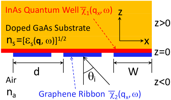
To uncover the physical mechanism behind the reported graphene-plasmon peak shift with GMRA period ju , we show a comparison in Fig. 2 for two calculated far-field transmissivity spectra , defined by Eq. (72), as a function of photon energy with m (red solid curve) and m (blue dashed curve). Here, only the graphene micro-ribbon array is included in our system. As increases, the graphene plasmon peak at meV for m shifts down to meV for m and this peak shift accurately satisfies the scaling relation experimentally observed ju . A series of kinks below the plasmon peak in Fig. 2 corresponds to the single-particle excitations at (for ) with for different values of integer . On the other hand, the shoulder appearing above the dominant peak comes from another severely-Landau-damped graphene-plasmon peak, which becomes more visible for m since the peak separation is increased.
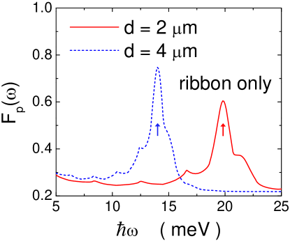
To see the many-body effect on the hybridized GMRA-QW plasmon excitation, Fig. 3 presents a comparison for as a function of with two values for the graphene chemical potential, i.e., eV (red solid curve) and eV (blue dashed curve). Here, the chemical potential of graphene ribbons can be tuned by a gate voltage ju . As expected, one of the two graphene-like plasmon peaks at meV for eV moves up to meV for eV. Interestingly, from this hybridized GMRA-QW plasmon peak shift we find that the plasmon energy is not scaled as , which is different from the observation reported in Ref. ju, for the ribbon-only case. However, our calculated graphene plasmon peak shift (from meV to meV) for the ribbon-only case (not shown here) fully agrees with their observation ju . The -insensitive plasmon peak at meV is associated with the SP excitation at the photon energy meV and will be addressed in Fig. 6 below. Additionally, when eV, we see a new strong graphene-like plasmon peak show up at meV because one relatively-flattened portion wunsch ; oleksiy on the plasmon dispersion curve at a relative large value becomes free of Landau-damping.
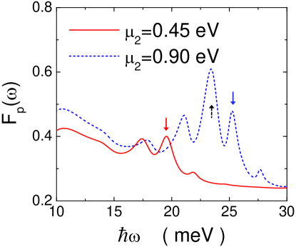
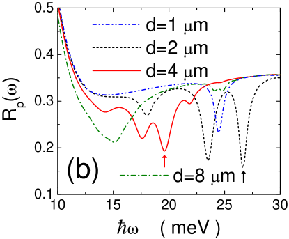
To further elucidate the importance of the EM coupling between the graphene plasmon in GMRA, as shown in Fig. 2, and the 2DEG plasmon in a QW, we displayed in Fig. 4 comparisons for [in (a)] and for the far-field reflectivity spectra , defined by Eq. (71), [in (b)] as functions of by choosing four different array periods: m (blue dash-dot-dotted curves), m (black dashed curves), m (red solid curves) and m (green dash-dotted curves). Here, we fixed the ratio of the ribbon width to the array period by . As indicated by two downward arrows in Fig. 4(a) for the shift of one of the two graphene-like plasmon peaks from meV for m to meV for m, we determine that the hybridized GMRA-QW plasmon energy is approximately proportional to for . When m, only two weakly-split plasmon peaks are visible at meV and meV, respectively. As decreases from m to m, the peak at meV for m is pushed up to meV. These peak shifts with GMRA period are also reflected in Fig. 4(b), as indicated by the two upward arrows for example, and the steep rise of around meV is associated with the excitation of SP mode in the system.
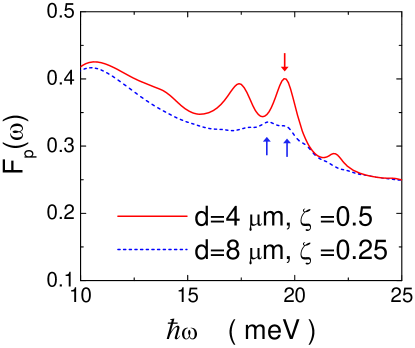
In order to clarify the fact that the graphene-like plasmon energy is actually proportional to , due to the non-locality in the optical response of interacting electrons, instead of in single-particle modes, we show in Fig. 5 for two cases with the same value for but different values for . For the case with and m, we find a weakly-split peak (indicated by two upward arrows), which is aligned with a strong non-split peak (indicated by a downward arrow) at and m. This clearly demonstrates that the graphene-like plasmon peak energy is proportional to instead of , which is again in agreement with the observation by Ju et al ju . The finite width of a ribbon introduces a characteristic wavenumber (proportional to ), which enforces a cut-off to the short-range coulomb interaction between electrons in a micro-ribbon. A smaller value implies a weaker coupling between the 2DEG and graphene plasmon excitations. The splitting of the plasmon peak for is attributed to the contribution of even-integer diffraction modes, while only odd-integer diffraction modes can contribute for , as can be verified by the –terms appearing in Eqs. (54) and (55).
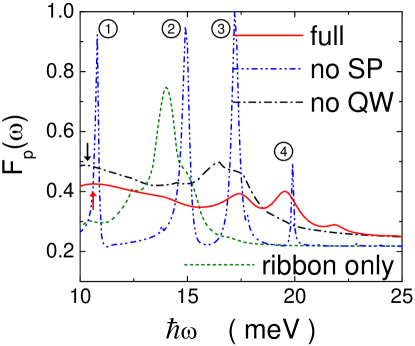
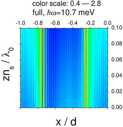
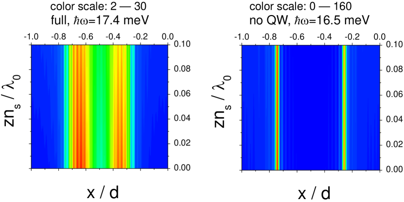
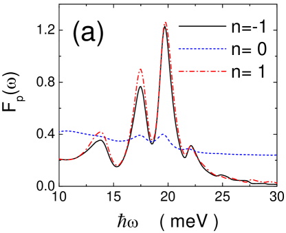
Figure 6 presents in the left panel the individual and combined effects of SP, 2DEG and GMRA as well as the strong EM coupling among these plasmon excitations. The periodicity of GMRA opens a minigap between any two adjacent branches (Bloch modes) in a folded hybridized-plasmon dispersion curve. These minigaps can be opened either at the Brillouin-zone center or at the Brillouin-zone boundary. In the deep sub-wavelength regime, only the minigap at the Brillouin-zone center leads to a peak in the far-field transmissivity spectrum aam1 . When the doped GaAs substrate is changed into an undoped one (no SP, blue dash-dot-dotted curve), only 2DEG and graphene plasmons can exist in this system. In this case, there exists strong EM coupling between the graphene and 2DEG plasmon excitations. As labeled by the circled numbers, peak–1 and peak–4 are related to the 2DEG-like plasmons, while peak–2 and peak–3 are connected to the graphene-like plasmon excitations. Two small kinks on the outer shoulders of peak–2 and peak–3 are a result of two induced anti-crossing gaps between coupled 2DEG-like and graphene-like plasmons. If the 2DEG in an InAs QW is removed from our system (no QW, black dash-dotted curve), we observe that the SP peak is strengthened in comparison with the full system (red solid curve) and shifted towards the left (indicated by two solid-line arrows) due to turning-off the 2DEG plasmon and its coupling to the SP in the system. Furthermore, the graphene-like plasmon peaks superposed on the shoulder of the SP peak become greatly weakened due to the loss of the strong coupling between the 2DEG and graphene plasmons. Here, a simple Drude-type optical-conductivity model ziegler ; soljacic cannot be applied to our system due to the large wavenumber involved in the deep sub-wavelength regime for a higher-order diffracted EM field. When only the GMRA exists in the system (ribbon only, green dashed curve), a downward-shifted dominant plasmon peak at meV, along with several kinks (a shoulder) below (above) the peak, show up in this panel, as explained in Fig. 2. From this figure we know that the graphene-ribbon effect can be best observed from hybridized GMRA-QW plasmon modes in the absence of the SP. In the lower panel of Fig. 6, we display the calculated transmitted –polarized E-field intensity at meV for the full system. In this case, a resonant SP effect on the intensity distribution is expected around the QW-mediated air/GaAs interface. Indeed, the intensity in the gap between two neighboring graphene micro-ribbons, where the QW-mediated air/GaAs interface is hosted, decreases greatly due to strong optical absorption by the SP ( meV). At the same time, the intensity is built up at two edges of a micro-ribbon and spreads out to the regions covered by micro-ribbons. A slight asymmetry in the intensity distribution with respect to the left and right edges of the gap region is attributed to a finite incident angle ().
In the presence of an SP, we compare the transmitted –polarized E-field intensities in Fig. 7 for the cases of with a QW at meV (left panel) or without a QW at meV (right panel). From the right panel of this figure, we find in the near-field regime that a GMRA tends to build up very strong E-field intensities just at two edges of a micro-ribbon. On the other hand, the QW would like to spread the E-field intensity across the gap region between two neighboring micro-ribbons although two close-magnitude maxima in intensity distribution can still be seen between the gap center and edges. The competition of these two opposite effects constitutes a strong EM coupling between the 2DEG and graphene plasmon excitations, as shown in the upper panel of Fig. 6. In addition, we notice that the E-field intensity for both panels is a little higher at the left edge of the gap region for the lower of the two graphene-like plasmon peaks in Fig. 6.
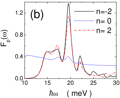
To find the strongly-diffracted near-field effect in the deep sub-wavelength regime, as shown in Fig. 7, on the far-field transmissivity spectrum, we compare in Fig. 8 the calculated partial near-field transmissivity spectra for polarization, defined by Eq. (74), with [in (a)] and [in (b)]. It is clear from Figs. 8(a) and (b) that the graphene-like plasmon peak at meV mainly comes from the contributions of the diffraction modes with , while the plasmon peak at meV is produced jointly by the diffraction modes with both and . In general, the peak in the near-field transmissivity spectrum (black solid and red dash-dotted curves) can be much stronger than that in the far-field spectrum (blue dashed curves) due to the very strong near-field intensity as displayed in Fig. 7. The non-locality in the optical response of electrons, as given by Eqs. (27) and (29), facilitates the mixing between the EM-field specular and diffraction modes, which enables transferring the peak weight from a near field to a far field. We also note that the peak strengths for the diffraction modes associated with are close in magnitude in this figure.
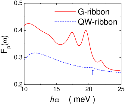
Surprisingly, for an inverted structure (QW-ribbon, blue dashed curve), where the graphene ribbons become a graphene sheet while the InAs QW sheet becomes QW ribbons, we find from Fig. 9 that the SP effect is greatly suppressed, compared to the original system (G-ribbon, red solid curve), in addition to an overall reduction of peak strength in the transmissivity. However, the EM-field reflectivity is found to be enhanced (not shown here) in this inverted structure for the range of photon energies shown in the figure. In this case, only one very weak peak at meV is visible for the inverted structure, which is attributed to an order-of-magnitude lower electron density in the QW compared to that in a graphene micro-ribbon. At the same time, the SP-related peak shifts from meV to meV due to switching from the QW-SP coupling to the graphene-sheet-SP coupling.
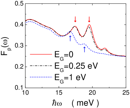
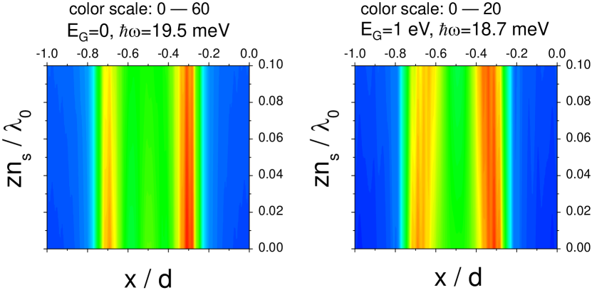
We display in the upper panel of Fig. 10 the effect of bandgap on with (red solid curve), eV (black dash-dotted curve) and eV (blue dashed curve). Since a finite leads to an effective mass () for electrons close to the band edge, its effect on is expected to be substantial (see Fig. 9) as . Indeed, we find from the upper panel that the strengths of the two graphene-like plasmon peaks are significantly reduced when eV (for eV). Correspondingly, from the lower panel of this figure, we see a decrease of near-field intensity as well as an enhanced EM coupling between the 2DEG and graphene plasmons, i.e. the E-field intensity spreads inward from the two edges to the center of the gap region.
IV Conclusions
In conclusion, we have derived in this paper a self-consistent theory involving Maxwell equations to determine a total EM field and the density-matrix linear-response theory to determine an induced optical-polarization field. We have applied this self-consistent theory to study a model system composed of an electronically-isolated two-dimensional electron gas and an electron-doped graphene micro-ribbon array on the surface of an -doped semi-infinite semiconductor substrate. The numerical results for the transmissivity and reflectivity spectra in the presence of an incident plane wave have been compared and physically explained in the deep sub-wavelength regime for various linear-array period, micro-ribbon width, doped graphene chemical potential and different configurations of our model system. Our calculations have demonstrated the existence of a tunable EM coupling among the localized surface, conventional electron-gas and massless graphene intraband collective excitations in the deep sub-wavelength regimes for terahertz frequencies.
Acknowledgments
This research was supported by the Air Force Office of Scientific
Research (AFOSR).
Appendix A
| (75) |
where the source column vector is found to be
| (76) |
If we limit , we can write down the unknown column vector as
| (77) |
Moreover, elements of the coefficient matrix introduced in Eq. (75) can be written out explicitly as
| (79) |
| (81) |
| (83) |
where , , , , and
| (85) |
where , and .
For , we have
| (87) |
with , while for , we acquire
| (89) |
with .
In addition, for , this gives
| (91) |
where , , , and , while for , it leads to
| (93) |
where , , , and .
Finally, for , this yields
| (95) |
where , , , and , while for , one is left with
| (97) |
where , , , and .
For our numerical calculations in this paper, we take
to ensure the accuracy of the presented results.
References
- (1) A. H. C, Neto, F. Guinea, N. M. R. Peres, K. S. Novoselov, and A. K. Geim, “The electronic properties of graphene”, Rev. Mod. Phys. 81, 109-162 (2009).
- (2) Special issue on “Electronic and photonic properties of graphene layers and carbon nanoribbons”, (Edited by G. Gumbs, D. H. Huang and O. Roslyak), Phil. Trans. R. Soc. A 138, No. 1932 (2010).
- (3) D. S. L. Abergel, V. Apalkov, J. Berashevich, K. Ziegler, and T. Chakraborty, “Properties of graphene: a theoretical perspective”, Adv. Phys. 59, 261-482 (2010).
- (4) M. Orlita and M. Potemski, “Dirac electronic states in graphene systems: optical spectroscopy studies”, Semicond. Sci. Technol. 25, 063001 (2010).
- (5) S. Das Sarma, S. Adam, E. H. Hwang, and E. Rossi, “Electronic transport in two-dimensional graphene”, Rev. Mod. Phys. 83, 407-470 (2011).
- (6) K. S. Novoselov, A. K. Geim, S. V. Morozov, D. Jiang, M. I. Katsnelson, I. V. Grigorieva, S. V. Dubonos, and A. A. Firsov, “Electric field effect in atomically thin carbon films”, Sci. 306, 666-669 (2004).
- (7) K. S. Novoselov, A. K. Geim, S. V. Morozov, D. Jiang, M. I. Katsnelson, I. V. Grigorieva, S. V. Dubonos, and A. A. Firsov, “Two-dimensional gas of massless Dirac fermions in graphene”, Nat. 438, 197-200 (2005).
- (8) Y. Zhang, Y.-W. Tan, H. L. Störmer, and P. Kim, “Experimental observation of the quantum Hall effect and Berry’s phase in graphene”, Nat. 438, 201-204 (2005).
- (9) M. I. Katsnelson, K. S. Novoselov, and A. K. Geim, “Chiral tunnelling and the Klein paradox in graphene”, Nat. Phys. 2, 620-625 (2006).
- (10) A. F. Young and P. Kim, “Quantum interference and Klein tunnelling in graphene”, Nat. Phys. 5, 222-226 (2009).
- (11) O. Roslyak, A. Iurov, G. Gumbs, and D. H. Huang, “Unimpeded tunneling in graphene nanoribbons”, J. Phys.: Condens. Matt. 22, 165301 (2010).
- (12) A. Iurov, G. Gumbs, O. Roslyak, and D. H. Huang, “Anomalous photon-assisted tunneling in graphene”, J. Phys.: Condens. Matt. 24, 015303 (2012).
- (13) B. Wunsch, T. Stauber, F. Sols, and F. Guinea, “Dynamical polarization of graphene at finite doping”, New J. Phys. 8, 318 (2006).
- (14) E. H. wang and S. Das Sarma, “Dielectric function, screening, and plasmons in two-dimensional graphene”, Phys. Rev. B 75, 205418 (2007).
- (15) O. Roslyak, G. Gumbs, and D. H. Huang, “Plasma excitations of dressed Dirac electrons in graphene layers”, J. Appl. Phys. 109, 113721 (2011).
- (16) K. F. Mak, M. Y. Sfeir, Y. Wu, C. H. Lui, J. A. Misewich, and T. F. Heinz, “Measurement of the Optical Conductivity of Graphene”, Phys. Rev. Lett. 101, 196405 (2008).
- (17) R. R. Nair, P. Blake, A. N. Grigorenko, K. S. Novoselov, T. J. Booth, T. Stauber, N. M. R. Peres, and A. K. Geim, “Fine Structure Constant Defines Visual Transparency of Graphene”, Sci. 320, 1308 (2008).
- (18) L. Ju, B. Geng, J. Horng, C. Girit, M. Martin, Z. Hao, H. A. Bechtel, X. Liang, A. Zettl, Y. R. Shen and F. Wang, “Graphene plasmonics for tunable terahertz metamaterials”, Nat. Nanotechn. 6, 630-634 (2011).
- (19) Z. Q. Li, E. A. Henriksen, Z. Jiang, Z. Hao, M. C. Martin, P. Kim, H. L. Störmer, and D. N. Basov, “Dirac charge dynamics in graphene by infrared spectroscopy”, Nat. Phys. 4, 532-535 (2008).
- (20) F. Wang, Y. Zhang, C. Tian, C. Girit, A. Zettl, M. Crommie, and Y. R. Shen, “Gate-Variable Optical Transitions in Graphene”, Sci. 320, 206-209 (2008).
- (21) Q. Bao, H. Zhang, B. Wang, Z. Ni, C. Haley, Y. X. Lim, Y. Wang, D. Y. Tang, and K. P. Loh, “Broadband graphene polarizer”, Nat. Photonics, 5, 411-415 (2011).
- (22) J. H. Strait, H. Wang, S. Shivaraman, V. Shields, M. Spencer, and F. Rana, “Hot Carrier Transport and Photocurrent Response in Graphene”, Nano Lett. 11, 4688-4692 (2011).
- (23) J. C. W. Song, M. S. Rudner, C. M. Marcus, and L. S. Levitov, “Very Slow Cooling Dynamics of Photoexcited Carriers in Graphene Observed by Optical-Pump Terahertz-Probe Spectroscopy”, Nano Lett. 11, 4902-4906 (2011).
- (24) O. Roslyak, G. Gumbs, and D. H. Huang, “Tunable band structure effects on ballistic transport in graphene nanoribbons”, Phys. Lett. A 374, 4061-4064 (2010).
- (25) D. H. Huang, G. Gumbs, and O. Roslyak, “Field enhanced mobility by nonlinear phonon scattering of Dirac electrons in semiconducting graphene nanoribbons”, Phys. Rev. B 83, 115405 (2011).
- (26) O. Roslyak, G. Gumbs, and D. H. Huang, “Energy loss spectroscopy of epitaxial versus free-standing multilayer graphene”, Physica E 44. 1874-1884 (2012).
- (27) J. Z. Bernád, M. Jääskeläinen, and U. Zülicke, “Effects of a quantum measurement on the electric conductivity: Application to graphene”, Phys. Rev. B 81, 073403 (2010).
- (28) K. Nomura and A. H. MacDonald, “Quantum Hall Ferromagnetism in Graphene”, Phys. Rev. Lett. 96, 256602 (2006).
- (29) T. Fang, A. Konar, H. Xing, and D. Jena, “Mobility in semiconducting graphene nanoribbons: Phonon, impurity, and edge roughness scattering”, Phys. Rev. B 78, 205403 (2008).
- (30) A. Bostwick, F. Speck, T. Seyller, K. Horn, M. Polini, R. Asgari, A. H. MacDonald, and E. Rotenberg, “A Catalog of Reference Genomes from the Human Microbiome”, Sci. 328, 994-999 (2010).
- (31) S. A. Mikhailov and K. Ziegler, “New Electromagnetic Mode in Graphene”, Phys. Rev. Lett. 99, 016803 (2007).
- (32) M. Jablan, H. Buljan, and M. Soljačić, “Plasmonics in graphene at infrared frequencies”, Phys. Rev. B 80, 245435 (2009).
- (33) G. Gumbs and D. H. Huang, Properties of Interacting Low-Dimensional Systems (Wiley-VCH Verlag GmbH & Co. kGaA, Weinheim, Germany, 2011), Chaps. 4 and 5.
- (34) D. H. Huang, C. Rhodes, P. M. Alsing, and D. A. Cardimona, “Effects of longitudinal field on transmitted near field in doped semi-infinite semiconductors with a surface conducting sheet”, J. Appl. Phys. 100, 113711 (2006).
- (35) D. H. Huang, G. Gumbs, P. M. Alsing, and D. A. Cardimona, “Nonlocal mode mixing and surface-plasmon-polariton-mediated enhancement of diffracted terahertz fields by a conductive grating”, Phys. Rev. B 77, 165404 (2008).
- (36) D. H. Huang, G. Gumbs, and S.-Y. Lin, “ Self-consistent theory for near-field distribution and spectrum with quantum wires and a conductive grating in terahertz regime”, J. Appl. Phys. 105, 093715 (2009).
- (37) D. H. Huang and D. A. Cardimona, “Effects of off-diagonal radiative-decay coupling of electron transitions in resonant double quantum wells”, Phys. Rev. A 64, 013822 (2001).
- (38) D. H. Huang, T. Apostolova, P. M. Alsing, and D. A. Cardimona, “High-field transport of electrons and radiative effects using coupled force-balance and Fokker-Planck equations beyond relaxation-time approximation”, Phys. Rev. B 69, 075214 (2004).
- (39) D. H. Huang, P. M. Alsing, T. Apostolova, and D. A. Cardimona, “Effect of photon-assisted absorption on the thermodynamics of hot electrons interacting with an intense optical field in bulk GaAs”, Phys. Rev. B 71, 045204 (2005).
- (40) D. H. Huang, P. M. Alsing, T. Apostolova, and D. A. Cardimona, “Coupled energy-drift and force-balance equations for high-field hot-carrier transport”, Phys. Rev. B 71, 195205 (2005).
- (41) P. M. Platzman and P. A. Wolff, Waves and Interactions in Solid State Plasmas, (Academic, New York, 1973).
- (42) J. M. Pitarke, V. M. Silkin, E. V. Chulkov, and P. M. Echenique, “Theory of surface plasmons and surface-plasmon polaritons”, Rep. Prog. Phys. 70 1-87 (2007).
- (43) A. V. Zayats, I. I. Smolyaninov, and A. A. Maradudin, “Nano-optics of surface plasmon polaritons”, Phys. Rep. 408, 131-314 (2005).
- (44) G. Gumbs, D. H. Huang, and D. N. Talwar, “Doublet structure in the absorption coefficient for tunneling-split intersubband transitions in double quantum wells”, Phys. Rev. B 53, 15436-15439 (1996).
- (45) L. Brey and H. A. Fertig, “Elementary electronic excitations in graphene nanoribbons”, Phys. Rev. B 75, 125434 (2007).
- (46) F. Stern, “Polarizability of a Two-Dimensional Electron Gas”, Phys. Rev. Lett 18, 546-548 (1967).
- (47) M. A. H. Vozmediano and F. Guinea, “Effect of Coulomb interactions on the physical observables of graphene”, Phys. Scr. T146, 014015 (2012).
- (48) D. C. Elias, R. V. Gorbachev, A. S. Mayorov, S. V. Morozov, A. A. Zhukov, P. Blake, L. A. Ponomarenko, I. V. Grigorieva, K. S. Novoselov, F. Guinea and A. K. Geim, “Dirac cones reshaped by interaction effects in suspended graphene”, Nat. Phys. 7, 701-704 (2011).
- (49) B. Y.-K. Hu, E. H. Hwang and S. Das Sarma, “Density of states of disordered graphene”, Phys. Rev. B 78, 165411 (2008).
- (50) K. S. Gupta and S. Sen, “Bound states in gapped graphene with impurities: Effective low-energy description of short-range interactions”, Phys. Rev. B 78 205429 (2008).
- (51) B. Baumeier, T. A. Leskova and A. A. Maradudin, “Transmission of light through a thin metal film with periodically and randomly corrugated surfaces”, J. Opt. A: Pure Opt. 8, S191-S207 (2006).