Spin Symmetry of the Bilayer Graphene Groundstate
Abstract
We show nonlinear transport experiments on clean, suspended bilayer graphene that reveal a gap in the density of states. Looking at the evolution of the gap in magnetic fields of different orientation, we find that the groundstate is a spin-ordered phase. Of the three possible gapped groundstates that are predicted by theory for equal charge distribution between the layers, we can therefore exclude the quantum anomalous Hall phase, leaving the layer antiferromagnet and the quantum spin Hall phase as the only possible gapped groundstates for bilayer graphene.
pacs:
72.80 Vp, 73.22 Gk, 73.22 Pr, 73.23.-b, 73.43 QtThe isolation of monolayer graphene Novoselov et al. (2004) has given a new twist to the research on two-dimensional electron systems, because graphene as a zero-gap semiconductor with a pseudo-relativistic dispersion relation shows fundamentally new effects such as Klein-tunneling Katsnelson et al. (2006) that do not occur in conventional two-dimensional electron gases (2DEGs) with a finite bandgap and a parabolic dispersion. The presence of two atoms in the graphene unit cell is described by a sublattice-pseudospin, which acquires a Berry phase of on closed k-space trajectories that include one of the K-points, which are the corner points of the first Brioullin zone and also constitute the Fermi surface of charge neutral graphene. One consequence of this Berry phase is an unusual Landau level spectrum that leads to the occurence of quantum Hall plateaus at conductances of half integer multiples of the Landau level degeneracy Novoselov et al. (2005); Zhang et al. (2005). As the pseudospin degree of freedom is present also in Bernal stacked graphene multilayers, they can be described by one low energy theory that explicitly includes the chiral nature of the charge carriers Min and MacDonald (2008).
Bilayer graphene in A-B stacking is a 2DEG with a parabolic dispersion for small energies , where 0.4 eV is the interlayer hopping parameter that links two atoms sitting on top of each other McCann and Fal’ko (2006). As a consequence of the parabolic dispersion there is a finite density of states at the charge neutrality point (CNP) which, together with the weak dispersion leads to strong electron-electron interactions that make bilayer graphene at the CNP unstable towards interaction induced symmetry breaking Min et al. (2008); Barlas and Yang (2009); Zhang et al. (2010); Nandkishore and Levitov (2010a, b); Vafek and Yang (2010); Lemonik et al. (2010).
The exact nature of the electronic groundstate of bilayer graphene at charge neutrality is being discussed intensely at the moment, with numerous theoretical investigations suggesting a large number of phases. In each of these phases some of the three discrete degrees of freedom in bilayer graphene (spin, valley and layer) undergo a transition to a lower symmetry state. While it is clear that for large magnetic fields quantum Hall ferromagnetism will occur Barlas et al. (2008), and that for strong perpendicular electric fields a layer polarized state will form Min et al. (2008); Jung et al. (2011), the nature of the groundstate at B=0 and E⟂=0 is less obvious. Whereas some experiments have found a conductive groundstate Mayorov et al. (2011); Bao et al. (2012), the majority of experimental results Feldman et al. (2009); Weitz et al. (2010); Velasco et al. (2012); Bao et al. (2012); Freitag et al. (2012a, b); van Elferen et al. (2012); Veligura et al. (2012) point to an insulating groundstate, an observation that limits the number of possible phases to the ones that are bulk gapped.
In this communication we show experimental results that further elucidate the nature of the bilayer graphene groundstate. We have performed nonlinear conductance measurements at the CNP of clean, suspended bilayer graphene samples as a function of magnetic fields oriented perpendicular and parallel to the graphene layer. Our measurements show a gap, that increases strongly only in a perpendicular magnetic field, whereas it stays constant to a high precision in a magnetic field that is exactly parallel to the bilayer plane. Our results allow us to make a statement about the spin order of the bilayer graphene groundstate and therefore to narrow down further the number of possible candidates for the electronic groundstate of bilayer graphene.
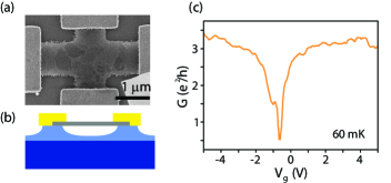
Bilayer graphene was exfoliated from natural graphite onto oxidized silicon wafers, and contacted with Cr/Au electrodes using e-beam lithography. The bilayer was suspended by partly removing the oxide in a buffered hydrofluoric acid wet etch and subsequent critical point drying, as described in Freitag et al. (2012b). The data shown here were obtained on a four-terminal sample in Hall-cross geometry that had been shaped by an Ar/O2 plasma dry etching process (figure 1). We measured two-terminal conductance on contacts on opposite sides of the Hall-cross with the other two terminals floating or connected to a high-impedance voltmeter for Hall measurements. All measurements were done in a dip-stick dilution refrigerator at base temperature (T=60 mK).
Figure 1 shows an SEM picture (a) and a schematic cross section (b) of the sample, together with backgate characteristics of the device (c) measured at T=60 mK after current annealing Freitag et al. (2012b). The charge neutrality point (CNP) is visible as a deep minimum in the conductance G measured as a function of gate voltage Vg at -0.6 V, indicating the formation of an insulating state around charge neutrality. The position of the CNP at a small negative gate voltage indicates a very small amount of residual dopants on the flake.
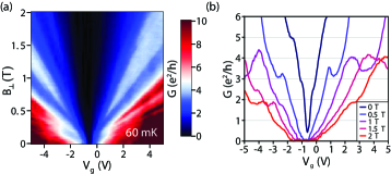
Figure 2a shows a measurement of the zero-bias conductance G as a function of gate voltage Vg and perpendicular magnetic field B⟂. From the line cuts in figure 2b one can see that there is a quantum Hall state at filling factor =4 developed for B 1.0T, giving a lower limit of 10 000 cm2/Vs for the charge carrier mobility. At higher fields additional intermediate plateaus start to occur, indicating a lifting of the spin and valley degeneracies.
Differential conductance Gd=dI/dV at the CNP as a function of perpendicular magnetic field and bias voltage Vsd is shown in figure 3a. Several line-cuts at different magnetic fields are shown in figure 3b. Similar to previous studies Velasco et al. (2012); Freitag et al. (2012a, b), we find a strong suppression of conductance around zero bias, together with a BCS-like overshoot at a finite voltage of V 3.5 mV, indicating the formation of an interaction induced broken symmetry state with a bulk gap.
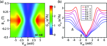
The Gd(Vsd) curves in figure 3b show two inflection points that we associate with two different gap energy scales and Freitag et al. (2012a, b). Following the inflection points in finite perpendicular magnetic field, we find that the larger feature increases linearly with 3.1 meV/tesla, whereas the smaller feature shows a weaker response of 1.7 meV/tesla, both of them however still much larger than the Zeeman energy for free electrons, which would amount to 0.116 meV/tesla 111Note that in our previous nomenclatureFreitag et al. (2012a, b), the present sample falls into category B2a.. As we have shown in previous studies Freitag et al. (2012a, b) the larger feature only exists in a narrow range of gate voltage around the CNP, whereas the small feature persists over the whole gate range that is accessible with the present sample. We think that is due to localization in disordered areas on the sample perimeter, and that has to be associated with an interaction induced broken symmetry state located in the center region of the sample.
Interaction effects in bilayer graphene have been described with the so-called broken symmetry state quasiparticle Hamiltonian
| (1) |
with , the effective mass, the layer pseudospin vector, + and - chosen for valley K and K’, respectively, and the order parameter of the broken symmetry state Min et al. (2008); Nandkishore and Levitov (2010a); Zhang et al. (2010, 2011); Velasco et al. (2012). For the groundstate is gapped and equation (1) predicts all electrons of the same spin and valley (the same spin-valley flavour) to be located in the same layer, a state that has also been described as a layer pseudospin magnet Min et al. (2008). Eight qualitatively different groundstates with distinct distributions of the four spin-valley flavors across the two layers are possible. Three of them have no overall layer polarization, and can be assumed to be energetically favorable in case of vanishing external electric fields. These three states are the quantum anomalous Hall state (QAH)Nandkishore and Levitov (2010b), the layer antiferromagnetic state (LAF), and the quantum spin Hall insulator (QSH). Their symmetries are determined by different order parameters in the quasiparticle Hamiltionian (1), namely for the QAH, for the LAF, and for the QSH. Here and represent the valley pseudospin and the electron spin, respectively. Due to a peculiar k-space topology Zhang et al. (2011), each spin valley flavor has an intrinsic Hall conductivity, the direction of which is given by sign(): It depends on the valley and the sign of the order parameter in equation (1). While for the LAF and QSH states the (charge) Hall conductivities of the four different spin-valleys cancel out, in the QAH they add up, which means that for the QAH a nonzero quantized Hall conductance of 4e2/h is expected even in the absence of an external magnetic field. Although no net charge Hall conductivity is expected for the QSH phase, the resulting edge states will be helical, leading to a quantized spin Hall effect. More important, both QAH and QSH are expected to show a conductance of 4e2/h in a two-terminal transport experiment, in case the edge-states couple to the metallic contacts. However, as we have shown in a previous publication Freitag et al. (2012b), this condition is not necessarily fulfilled in experiment, as the clean part of a sample that hosts the gapped phase can be separated from the metallic contacts by a more disordered phase. This disordered phase will not let edge-states penetrate to the contacts, but will confine them to isolated puddles in the sample center. For the LAF charge, spin and valley Hall conductances cancel out, no edge-states can form, and consequently LAF is expected to be fully insulating even in a two-terminal conductance measurement. Ignoring the effect of the magnetic field on the electron spins the LAF state has also been predicted to show a gap whose size is independent of a perpendicular magnetic field, whereas QAH and QSH should show a strong increase of the gap by 5.5 meV/tesla Velasco et al. (2012). A theory including spin Kharitonov (2012) however predicts the formation of a canted antiferromagnet (CAF) that shows a magnetic field dependence similar to that of QAH and QSH.
To identify the actual groundstate among the three candidates, it is useful to explore the three symmetries that might be preserved in them, namely time reversal symmetry , spin rotation symmetry (SU2), and valley Ising symmetry () Zhang et al. (2011); Velasco et al. (2012). In each of the three phases, only one symmetry is preserved: time-reversal symmetry in the QSH, spin rotational symmetry SU2 in the QAH, and valley Ising symmetry for the LAF.
The valley Ising symmetry , a state being invariant under exchange of K and K’, is broken in QAH and QSH, but is difficult to assess in a transport experiment. Time reversal symmetry is broken by the QAH and LAF, and the case of QAH would manifest in a spontaneous Hall conductance at zero magnetic field, and in general as an inequivalence of G(B) and G(-B). In a real world sample however, puddles of different sign of the Hall conductance would exist next to each other, so that a spontaneous Hall conductance would be unobservable. Spin rotation symmetry SU2, which is broken in the QSH and LAF, with the spins in the bottom and top layer being locked into an antiferromagnetic arrangement, can easily be assessed by looking at the response of the gap to a parallel magnetic field, to exclude any orbital effects that are responsible for the big response to perpendicular field. While LAF is a real antiferromagnet, with the spins in the top and bottom layer pointing into opposite directions, the QSH also has to be considered a phase with antiferromagnetic spin order, however with the spin orientation being opposite for different valleys. In both LAF and QSH, the electron spins are not free to move, and a response to parallel magnetic field would be absent, as long as the Zeeman energy is smaller than the exchange interaction responsible for the antiferromagnetic spin arrangement Zhang and MacDonald (2012). In the QAH the electron spins are not ordered and would show a response to parallel field determined by the Zeeman spitting of the spin up and spin down levels. This would lead to a decrease of the gap by gB.
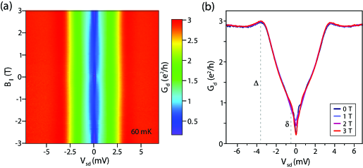
In order to assess the response of to a parallel magnetic field, we have performed nonlinear conductance measurements in a vector magnet system that allowed adjusting the orientation of the magnetic field vector with high precision. As the Zeeman splitting of the conduction electrons with g=2 is much smaller than the response of to a perpendicular magnetic field, the proper adjustment of the direction of B∥ is crucial, and a small misalignment of a few degrees will lead to a perpendicular field component that will change much more than what is expected from Zeeman splitting alone. Measurements were done with the sample mounted vertically, and B∥ was applied in the direction of the bilayer plane. As initial measurements showed an unreasonably large response of Gd(Vsd) to B∥(see supplementary information), we checked the correct alignment of the sample plane by applying an additional, small magnetic field in the horizontal direction, maximizing the height of the BCS-like overshoot visible in Gd(Vsd) at V 3.5 meV (see figures 3b, 4b and supplementary information). We found that the sample had a slight misalignment of 1.6o with respect to the vertical direction, probably due to mechanical imperfections of the sample holder. Adding a small horizontal field component to the vertical magnetic field, we were able to compensate for this misalignment and to adjust the magnetic field to the sample plane with a precision of 0.1o.
The results of a measurement of differential conductance at the CNP as a function of B∥ and Vsd are shown in figure 4. Compared to the conductance as a function of perpendicular field (figure 3) it is clear from figures 4a and 4b that the big gap is not affected by a parallel magnetic field. Following the outer inflection points at V2.5 mV we find a magnetic field dependence of less than 60 eV/tesla, which is significantly smaller than the electron spin Zeeman splitting of 116 eV/tesla (see supplementary information for details). Our experimental results therefore allow us to exclude a change of due to the Zeeman splitting of the conduction electrons. Note that a small dependence of Gd on occurs around zero bias V0. We think however that this change in does not originate from the clean phase in the sample center and is not related to the gap . According to the previous paragraph, this result shows that the electronic phase that we have labeled is a spin-ordered phase, where the electron spins are bound by some exchange interaction and do not respond to an external magnetic field. Looking at the spin properties of the three possible candidates for , we can conclude that is not the quantum anomalous Hall (QAH) state, but that it has to be one of the remaining two: the quantum spin Hall (QSH) or the layer antiferromagnet (LAF). To further distinguish QSH from LAF one could make use of the spin Hall effect in the QSH, which should lead to a finite spin accumulation on the Hall terminals of a Hall cross sample. Such a spin accumulation might be detectable via the inverse spin Hall effect, using a metal with strong spin-orbit scattering, such as palladium, as contact material on the Hall terminals. Due to the non optimal homogeneity of multi-terminal, current-annealed suspended graphene samples Freitag et al. (2012b), the significance of such an experiment would however have to be evaluated very carefully.
In conclusion by performing nonlinear transport experiments on clean bilayer graphene for magnetic fields of perpendicular and parallel orientation we have shown that the groundstate at charge neutrality is gapped, and is a spin ordered phase. Of the three possible broken symmetry states that are suggested by theory, we can exclude that a quantum anomalous Hall state is realized in bilayer graphene. The groundstate has to be either the quantum spin Hall state, or the layer antiferromagnetic state. To distinguish the latter two from each other, further experimental work will be needed.
Acknowledgements.
We acknowledge financial support by the Swiss NCCR on Nanoscience and Nanotechnology, the NCCR on Quantum Science and Technology, the ESF program Eurographene, the EU STREPS project SE2ND, and the Swiss National Science foundation.References
- Novoselov et al. (2004) K. S. Novoselov, A. K. Geim, S. V. Mozorov, D. Jiang, Y. Zhang, S. V. Dubonos, I. V. Grigorieva, and A. A. Firsov, Science 306, 666 (2004).
- Katsnelson et al. (2006) M. I. Katsnelson, K. S. Novoselov, and A. K. Geim, Nature Physics 2, 620 (2006).
- Novoselov et al. (2005) K. S. Novoselov, A. K. Geim, S. V. Morozov, D. Jiang, M. I. Katsnelson, I. V. Grigorieva, S. V. Dubonos, and A. A. Firsov, Nature 438, 197 (2005).
- Zhang et al. (2005) Y. Zhang, Y.-W. Tan, H. L. Stormer, and P. Kim, Nature 438, 201 (2005).
- Min and MacDonald (2008) H. Min and A. H. MacDonald, Phys. Rev. B 77, 155416 (2008).
- McCann and Fal’ko (2006) E. McCann and V. I. Fal’ko, Phys. Rev. Lett. 96, 086805 (2006).
- Min et al. (2008) H. Min, G. Borghi, M. Polini, and A. H. MacDonald, Phys. Rev. B 77, 041407 (2008).
- Barlas and Yang (2009) Y. Barlas and K. Yang, Phys. Rev. B 80, 161408 (2009).
- Zhang et al. (2010) F. Zhang, H. Min, M. Polini, and A. H. MacDonald, Phys. Rev. B 81, 041402 (2010).
- Nandkishore and Levitov (2010a) R. Nandkishore and L. Levitov, Phys. Rev. Lett. 104, 156803 (2010a).
- Nandkishore and Levitov (2010b) R. Nandkishore and L. Levitov, Phys. Rev. B. 82, 115124 (2010b).
- Vafek and Yang (2010) O. Vafek and K. Yang, Phys. Rev. B 81, 041401 (2010).
- Lemonik et al. (2010) Y. Lemonik, I. L. Aleiner, C. Toke, and V. I. Fal’ko, Phys. Rev. B 82, 201408 (2010).
- Barlas et al. (2008) Y. Barlas, R. Côtè, K. Nomura, and A. H. MacDonald, Phys. Rev. Lett. 101, 097601 (2008).
- Jung et al. (2011) J. Jung, F. Zhang, and A. H. MacDonald, Phys. Rev. B 83, 115408 (2011).
- Mayorov et al. (2011) A. S. Mayorov, D. C. Elias, M. Mucha-Kruczynski, R. V. Gorbachev, T. Tudorovskiy, A. Zhukov, S. V. Morozov, M. I. Katsnelson, V. I. Falko, A. K. Geim, et al., Science 333, 860 (2011).
- Bao et al. (2012) W. Bao, J. Velasco Jr., F. Zhang, L. Jing, B. Standley, D. Smirnov, M. Bockrath, A. H. MacDonald, and C. N. Lau, PNAS 109, 10802 (2012).
- Feldman et al. (2009) B. E. Feldman, J. Martin, and A. Yacoby, Nature Phys. 5, 889 (2009).
- Weitz et al. (2010) R. T. Weitz, M. T. Allen, B. E. Feldman, J. Martin, and A. Yacoby, Science 330, 812 (2010).
- Velasco et al. (2012) J. Velasco, Jr., L. Jing, W. Bao, Y. Lee, P. Kratz, V. Aji, M. Bockrath, C. N. Lau, C. Varma, R. Stillwell, et al., Nature Nanotech. 7, 156 (2012).
- Freitag et al. (2012a) F. Freitag, J. Trbovic, M. Weiss, and C. Schönenberger, Phys. Rev. Lett. 108, 076602 (2012a).
- Freitag et al. (2012b) F. Freitag, M. Weiss, R. Maurand, J. Trbovic, and C. Schönenberger, Solid State Comm. 152, 2053 (2012b).
- van Elferen et al. (2012) H. J. van Elferen, A. Veligura, E. V. Kurganova, U. Zeitler, J. C. Maan, N. Tombros, I. J. Vera-Marun, and B. J. van Wees, Phys. Rev. B 85, 115408 (2012).
- Veligura et al. (2012) A. Veligura, H. J. van Elferen, N. Tombros, J. C. Maan, U. Zeitler, and B. J. van Wees, Phys. Rev. B 85, 155412 (2012).
- Zhang et al. (2011) F. Zhang, J. Jung, G. A. Fiete, Q. Niu, and A. H. MacDonald, Phys. Rev. Lett. 106, 156801 (2011).
- Kharitonov (2012) M. Kharitonov, Phys. Rev. B 86, 195435 (2012).
- Zhang and MacDonald (2012) F. Zhang and A. H. MacDonald, Phys. Rev. Lett. 108, 186804 (2012).