Two Distinct Phases of Bilayer Graphene Films on Ru(0001)
pacs:
79.60.-i, 73.22.-f, 73.21.Cd, 81.05.Uw, 71.20.-bABSTRACT: By combining angle-resolved photoemission spectroscopy and scanning tunneling microscopy we reveal the structural and electronic properties of multilayer graphene on Ru(0001). We prove that large ethylene exposure allows to synthesize two distinct phases of bilayer graphene with different properties. The first phase has Bernal AB stacking with respect to the first graphene layer, displays weak vertical interaction and electron doping. The long-range ordered moiré pattern modulates the crystal potential and induces replicas of the Dirac cone and minigaps. The second phase has AA stacking sequence with respect to the first layer, displays weak structural and electronic modulation and p-doping. The linearly dispersing Dirac state reveals the nearly-freestanding character of this novel second layer phase.
The peculiar electronic properties of graphene result from its two-dimensional (2D) honeycomb crystal lattice. nov04 ; nov05 ; zha05 ; ber06 ; oht06 ; nov07 This 2D structure makes every carbon atom a surface atom and thus strongly exposed to the surrounding environment. The simple act of resting on a substrate may modify the electronic band structure and cause a precipitous decline of its charge carrier mobility. oht06 ; oos07 ; fei09 ; rut11 For example, when graphene is placed on top of another graphene layer in a Bernal (ABAB) stacking the coupling between the planes modifies the linear dispersion of the massless charge carriers into a hyperbolic dispersion of massive chiral fermions. gei07 ; mcc06 The graphene layers can be partially decoupled by misorienting them by more than 20∘ lui11 or by an AA stacking sequence. mak10 ; lob11 In these cases, the band structure has been predicted to be the superposition of two single-layer bands of freestanding graphene and only states with linear dispersion close to the Fermi level in proximity to the K points are present.
![[Uncaptioned image]](/html/1301.1610/assets/ToC.jpg)
Yet another way to preserve the electronic properties of graphene is to adsorb it on a material that has only very weak interaction with graphene. Recently, graphene supported on a hexagonal boron nitride substrate dea10 showed electrical properties comparable to that of freestanding graphene. On SiC(0001) oue10 ; bos07 ; haa08 and on Ni var08 ; yu08 ; rei09 the first graphene layer saturates the substrate bonds and allows the synthesis of subsequent graphene layers with nearly-freestanding character.
Another surface that strongly modifies graphene properties is Ru(0001). In this case, the first graphene layer relieves the strain due to the lattice mismatch between graphene and the substrate by developing a moiré structure. mar08 Core level spectroscopy, pre08 scanning tunneling microscopy (STM) mar07 ; mar08 ; wan08 ; mor10 ; str11 ; fen11 experiments and density functional theory calculations wan08 ; bru09 ; jia09 ; str11 ; fen11 ; ian11 have revealed spatial inhomogeneities in the charge density reflecting regions with varying graphene-substrate hybridization. Angle-resolved photoemission spectroscopy (ARPES) studies displayed a single and broad band with a relatively large gap. bru09 The first graphene layer saturates the metal bonds and acts as a template for the growth of a subsequent graphene layer with freestanding character sut08 ; esu09 which displays a sharp and linearly dispersing Dirac cone. sut09
Here, we provide evidence of a novel second layer phase on Ru(0001), which arises after exposure to more than 105 L ethylene that coexists with the hitherto reported phase. We compare ARPES data of the two second layer phases and find that the new phase gives rise to a second linearly dispersing band which is shifted with respect to the one of the first phase due to significant p-doping. Our STM data reveal that the two second layer phases have different stacking sequence and moiré amplitude.
RESULTS AND DISCUSSION
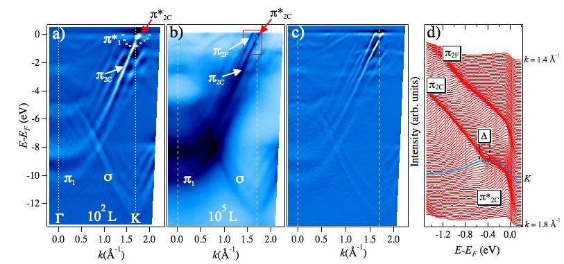
Figure 1(a) displays the second derivative of the ARPES intensity map along the direction of the graphene Brillouin zone after exposure to 102 L ethylene. We reproduce the previously observed relatively broad and bands and the sharp and states. In addition, we identify replica bands associated to the and states. In accordance with literature, sut09 we assign the bands as follows. The monolayer interacts strongly with the underlying substrate and displays a parabolic like dispersion of the state bru09 ; sut09 ; end10 ( band). This band has the minimum at =-10.1 eV at the point and the maximum at -4 eV at the K point. The strong interaction with the substrate also modifies the into a diffuse and faint band (enclosed by the white crosses in Figure 1(a)) in proximity to the Fermi level. The first layer saturates the metal orbitals and allows the growth of a second graphene layer which exhibits a sharp and n-doped Dirac cone, with the Dirac point at 0.450.05 eV below EF, along with replica and bands. sut08 ; esu09 ; sut09 ; end10 As will become clear from the STM data presented below, we refer to this layer as corrugated layer, therefore the label C.
Figures 1(b) and 1(c) show raw and second derivative ARPES maps recorded after exposing the 102 L surface to further 105 L ethylene. In addition to the first and corrugated second monolayer bands, we find a new state, which we call . F stands for flat layer, see below. The main features of this state are better captured in Figure 1(d) which displays energy distribution curves (EDCs) of the region marked by the red rectangle in Figure 1(b). The state disperses upward parallel to the state and crosses the Fermi level before the maximum is reached reminiscent of p-doping. By extrapolation of its linear dispersion we estimate the maximum of this band at 0.600.05 eV above the Fermi level. The constant gradient confirms the nearly-free character of the layers and yields an electron group velocity of m/s for both bands. Furthermore, EDC spectra highlight an electronic gap between the and states of 20030 meV at the K point (blue curve). This gap is also observed in the 102 L sample at variance with earlier measurements. sut09 ; end10
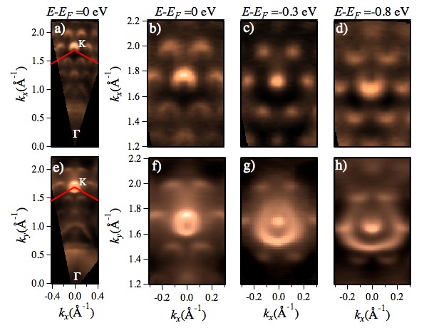
Figure 2 presents constant energy maps close to the K point of the graphene Brillouin zone and acquired on the low exposure (Figures 2(a)-2(d)) and high exposure samples (Figures 2(e)-2(h)). The Fermi surface of the 102 L sample displays the Dirac-like electron pocket of the state centered at the K point, and surrounded by hexagonally arranged replicas (Figures 2(a)-2(b)). The excellent long-range order of the surface allows to observe up to the third replica and to accurately measure the spacing between the replicas, amounting to Å-1. The electron density estimated from the relative size of the graphene Fermi surface with respect to the surface of Brillouin zone of graphite is 0.9 cm-2. For =-0.3 eV (Figure 2(c)), graphene bands are point-like, and then display hole pockets for 0.6 eV (Figure 2(d)). Similarly to graphene on SiC(0001), oht06 these replicas could be induced by diffraction effects due to the moiré of the first graphene layer, sut09 or as discussed later in the text, to the superlattice potential of the second graphene layer.
The Fermi surface of the 105 L sample in Figures 2(e) and 2(f) shows an additional Dirac-like hole pocket due to the band coexisting with the bands of the corrugated layer. The charge carrier concentration estimated from the relative size of the hole pocket is 2.5 holes per cm-2. With decreasing energies (Figures 2(g)-2(h)) the state spreads out in k-space without affecting the state.
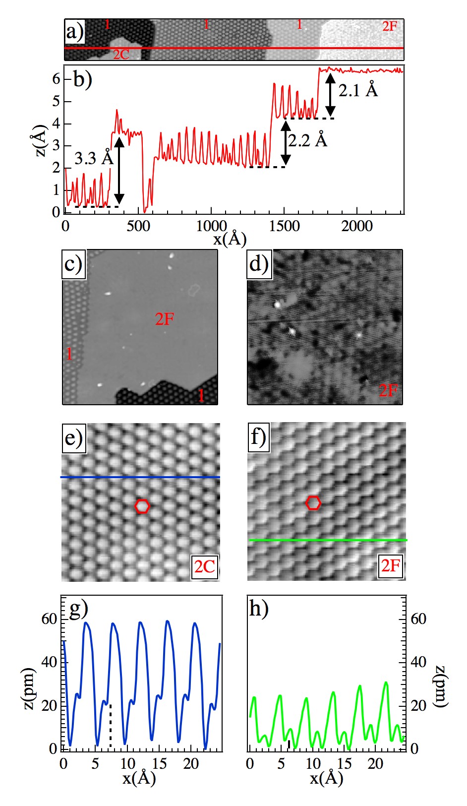
It is evident from comparison of the constant energy maps of both samples that the features of the 102 L sample appear at the same energies and positions in k-space also on the 105 L sample. Therefore the additional feature exhibited by the 105 L sample coexists but does not interact with the features. This is a notable difference with respect to multilayer graphene where the number of bands increases with the number of layers, but their dispersion gets modified by interlayer coupling. oht06 ; sut09 The absence of this interlayer coupling in the present case strongly suggests the coexistence of two second layer phases rather than the coexistence of second and a third monolayer. This conjecture is unequivocally proven by the following STM results recorded on a sample for which identical ARPES results as the ones shown in Figures 2(e)-(h) have been obtained. Figure 3(a) shows an STM image of the 105 L sample. The Ru surface is entirely covered by a well-ordered graphene first layer. This layer displays the moiré pattern mar08 ; pre08 ; bru09 ; sut09 ; sut08 resulting from the lattice mismatch between Ru and graphene. mar08 ; vaz08 ; mor10 Part of the first layer is covered by second layer graphene. On large scale images we clearly discern two types of second layer by their different moiré corrugation. A patch of the second layer type already reported in literature esu09 is visible in the lower left part of the image. It displays a moiré pattern with a maximum corrugation of 1.10 0.05 Å. It is therefore referred to as corrugated (C) layer and covers 122 % of the surface. The second type of the second layer is visible on the right hand side of Figure 3(a). It covers the 25 5 % of the first layer. Panel (c) shows that the 2F layer is essentially flat compared to the first monolayer. The STM image in Figure 3(d) shows the weak moiré contrast of the 2F layer. The apparent height amplitudes of the moiré patterns of the first, and 2F layers are 1.30 0.05, and 0.05 0.02 Å, respectively.
The line profile in Figure 3(b) demonstrates that 2C and 2F further distinguish themselves by their apparent heights with respect to the monolayer of 3.3 0.1 Å and 2.1 0.1 Å, respectively. The apparent height of a Ru(0001) step is 2.2 0.1 Å, in agreement with the literature value of 2.14 Å. The value measured for 2C corresponds to the distance of 3.3 Å between the atomic
layers in graphite which is Bernal, i.e., AB stacked. esu09 ; sun10 The AB stacking breaks the graphene sublattice symmetry while the AA stacking does not. Therefore high-resolution STM data can discern the two stackings, as evidenced by Figures 3(e) and (f) with their line profiles.
In Figure 3(e) the protrusions mark the centers of the C6 rings and the two carbon atoms per graphene unit cell are imaged as dark spots; The line profile taken along the blue line and displayed in Figure 3(g) evidences a difference in apparent height of 25 6 pm between these two atoms (vertical dotted line in Figure 3(g)). This lifting of the degeneracy between the A and B sublattices takes place in all the investigated regions of the corrugated layer and is responsible for the bandgap between the and states observed in Figure 1.
The apparent height between the first and the 2F layer is considerably smaller than the interlayer distance in graphite. However, in a previous STM work an apparent height of 2.5 Å has been observed between the first and the second graphene layer on SiC. rut07 High resolution transmission electron microscope studies reported a distance of 2.2 Å between two graphene layers grown on the (111) surface of diamond. lee08 This relatively small interlayer distance has been explained by an AA′ stacking, where alternate planes are translated by half the hexagonal cell width. In our case a shift between adjacent layers can be excluded since a detailed analysis of the atomic positions of first and flat second layer shows that they are in registry. cal
The AA stacking between the first and the 2F layer is further supported by the within the error bar identical apparent height of the two graphene sublattices reported in Figure 3(f). C atoms are again imaged dark. The apparent height difference between the two C sublattices in 2F layer has a mean value of 47 pm (vertical bar in Figure 3(h)). Therefore the STM data reveal a sublattice degeneracy for the 2F identical to free standing graphene while this degeneracy is clearly broken in the 2C.
We note that the apparent height of 2.1 0.1 Å for the 2F phase, is much smaller than the theoretical value expected for AA stacking of 3.66 Å. cha94
However, since STM probes the local density of states (LDOS), the measured apparent height can be significantly different from the interlayer distance if the layers are differently doped. Though the spot size of the photon beam does not allow us measuring the LDOS of the two bilayers separately, ARPES measurements reveal a different charge carrier concentration for the two bilayers due to a different charge transfer toward the first graphene layer. This different doping between the layers affects the STM measurements and may result in the much lower apparent height of the 2F layer with respect to the 2C layer.
The reasons why this second type of second graphene layer forms, and why it needs higher ethylene exposures to form can be attributed to the following. The difference in energy between the AB and AA staking is only 20 meV/atom, lee08 ; cha94 with AB stacking being more stable. This difference is sufficiently small, such that the AA stacking can be stabilized by kinetic effects which are more dominant under CVD growth with higher supersaturation.
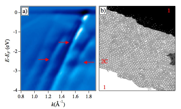
Finally, we discuss the nature of the replica bands observed for the state. Figure 4(a) show the first derivative of the band dispersion close to the K point for the 102 L sample. Replicas may arise by umklapp scattering from the moiré pattern of the first graphene layer. sut09 Note that graphene states also display breaks in the dispersion at the bands crossing (highlighted by red arrows) which reveal energy minigaps, similarly to graphene on Ir. ple09 ; rus10 ; pap12 Indeed, final state scattering enhances the photoemission intensity of the bands and may favor the resolution of the third order replicas by ARPES, however, the umklapp process cannot induce minigaps. These gaps are certainly due to a periodic perturbation to the crystal potential felt by the electrons in the initial state. This is supported by the STM measurement presented in Figure 4(b) revealing that the corrugated layer exhibits a long-range moiré pattern of period 2.7 nm. cal
CONCLUSION
In summary, we show evidence of a new phase of bilayer graphene on the Ru(0001) surface. Following massive ethylene exposure, ARPES spectra reveal a new state coexisting with the known ones which is reminiscent of a different interaction with the first graphene layer. STM investigations show that the Ru surface is fully covered by the first graphene layer which produces a strongly interacting band. On top of this layer, we find two phases of second graphene layer. One of the two (2C) exhibits Bernal stacking with respect to the first layer. This layer displays weak vertical interaction and a moiré pattern with marginal long-range order which modulates the crystal potential. This layer generates a sharp n-doped Dirac cone (), replica bands and minigaps. The other phase (2F) exhibits a single Dirac p-doped () state with nearly freestanding character. STM results show that this second layer phase is arranged in an AA stacking sequence with respect to the first layer and has a relatively weak structural and electronic modulation. We thus prove that the first layer can be used as a template to grow different phases of graphene bilayers.
METHODS
Measurements were performed in three different ultrahigh vacuum (UHV) chambers. The presented ARPES measurements were performed at the VUV-Photoemission beamline of the Elettra Synchrotron Facility in Trieste at 120 K, with a photon energy of 100 eV, and an energy resolution of 30 meV. The presented STM experiments were carried out at the Ecole Polytechnique Fédérale in Lausanne (EPFL) with a home-built low temperature scanning tunneling microscope operating at 0.4 K and used for the present study at 4 K. cla11 Additional ARPES and STM measurements were collected at the APE-IOM beamline of Elettra. This beamline has the STM and ARPES spectrometer connected in situ, so that complementary characterization of the same surfaces can be performed. At this endstation, the primary energy has been set to 65 eV whereas the other parameters have been kept identical, and the home-built STM has been operated at 300 K. All experiments were performed under UHV condition with a base pressure below Torr. The Ru(0001) crystal was cleaned by repeated cycles of Ar+ sputtering ( eV) and annealing at 1500 K. The order and cleanness of the sample was monitored by low-energy electron diffraction and photoemission spectroscopy at VUV and by STM measurements at EPFL and APE. A graphene bilayer was grown by exposing the Ru(0001) surface held at a temperature of 1600 K to L (1.9 Torr for 53 s) of ethylene (C2H4). nat12 The multiphase graphene bilayers were obtained by additional exposure to L (1.9 Torr for 530 s) ethylene with the Ru crystal at 1600 K. Samples that have been prepared and characterized at Elettra have been transported to Lausanne and imaged in STM with atomic resolution after a flash to 800 K in a pressure of Torr.
Acknowledgment. This work has been supported by the European Science Foundation (ESF) under the EUROCORES Program EuroGRAPHENE, by the Swiss National Science Foundation, and by the Italian Ministry of Education, University, and Research (FIRB Futuro in Ricerca, PLASMOGRAPH Project).
∗e-mail: marco.papagno@fis.unical.it
REFERENCES AND NOTES
References
- (1) Berger, C; Song, Z.; Li, X.; Wu, X.; Brown, N.; Naud, C.; Mayou, D.; Li, T.; Hass, J.; Marchenkov, A. N.; et al. Electron Confinement and Coherence in Patterned Epitaxial Graphene. Science 2006, 312, 1191-1196.
- (2) Novoselov, K. S.; Geim, A. K.; Morosov, S. V.; Jiang, D.; Zhang, Y.; Dubonos, S. V.; Grigorieva, I. V.; Firsov, A. A. Electric Field Effect in Atomically Thin Carbon Films. Science 2004, 306, 666-669.
- (3) Novoselov, K. S.; Geim, A. K.; Morozov, S. V.; Jiang, D.; Katsnelson, M. I.; Grigorieva, I. V.; Dubonos, S. V.; Firsov, A. A. Two-dimensional Gas of Massless Dirac Fermions in Graphene. Nature 2005, 438, 197-200.
- (4) Zhang, Y.; Tan, Y.W.; Stormer, H. L.; Kim, P. Experimental Observation of the Quantum Hall Effect and Berry s Phase in Graphene. Nature 2005, 438, 201-204.
- (5) Ohta, T.; Bostwick, A.; Seyller, T.; Horn, K.; Rotenber, E. Controlling the Electronic Structure of Bilayer Graphene. Science 2006, 313, 951-954.
- (6) Novoselov, K. S.; Jiang, Z.; Zhang, Y.; Morozov, S. V.; Stormer, H. L.; Zeitler, U.; Maan, J. C.; Boebinger, G. S.; Kim, P.; Geim, A. K. Room-Temperature Quantum Hall Effect in Graphene. Science 2007, 315, 1379-1379.
- (7) Bostwick, A.; Ohta, T.; Seyller, T.; Horn, K.; Rotenberg, E. Quasiparticle Dynamics in Graphene. Nat. Phys. 2007, 3, 36-40.
- (8) Oostinga, J. B.; Heersche, H. B.; Liu, X.; Morpurgo, A. F.; Vandersypen, L. M. K. Gate-Induced Insulating State in Bilayer Graphene Devices. Nature Mat. 2007, 7, 151-157.
- (9) Feldman, B. E.; Martin, J.; Yacobi, A. Broken-Symmetry States and Divergent Resistance in Suspended Bilayer Graphene. Nature Phys. 2009, 5, 889-893.
- (10) Rutter, G. M.; Jung, S.; Klimov, N. N.; Newell, D. B.; Zhitenev, N. B.; Stroscio, J. A. Microscopic Polarization in Bilayer Graphene. Nature Phys. 2011, 7, 649-655.
- (11) Geim, A. K.; Novoselov, K. S. The Rise of Graphene. Nat. Mater. 2007, 6, 183-191.
- (12) McCann, E. Asymmetry Gap in the Electronic Band Structure of Bilayer Graphene. Phys. Rev. B 2006, 74, 161403.
- (13) Luican, A.; Li, G.; Reina, A.; Kong, J.; Nair, R. R.; Novoselov, K. S.; Geim, A. K.; Andrei, E. Y. Single-layer Behavior and Its Breakdown in Twisted Graphene Layers. Phys. Rev. Lett. 2011, 106, 126802.
- (14) Mak, K. F.; Shan, J.; Heinz, T. F. Electronic Structure of Few-Layer Graphene: Experimental Demonstration of Strong Dependence on Stacking Sequence. Phys. Rev. Lett. 2010, 104, 176404.
- (15) Lobato, I.; Partoens, B. Multiple Dirac Particles in AA-Stacked Graphite and Multilayers of Graphene. Phys. Rev. B 2011, 83, 165429.
- (16) Dean, C. R.; Young, A. F.; Meric, I.; Lee, C.; Wang, L.; Sorgenfrei, S.; Watanabe, K.; Taniguchi, T.; Kim, P.; Shepard, K. L.; et al. Boron Nitride Substrates for High-Quality Graphene Electronics. Nature Nanotech. 2010, 5, 722-726.
- (17) Ouerghi, A.; Marangolo, M.; Belkhou, R.; El Moussaoui, S.; Silly, M. G.; Eddrief, M.; Largeau, L.; Portail, M.; Fain, B.; Sirotti, F. Epitaxial Graphene on 3C-SiC(111) Pseudosubstrate: Structural and Electronic Properties. Phys. Rev. B 2010, 82, 125445.
- (18) Hass, J.; de Heer, W. A.; Conrad, E. H. The Growth and Morphology of Epitaxial Multilayer Graphene. J. Phys.: Condens. Matter 2008, 20, 323202.
- (19) Varykhalov, A.; Snchez-Barriga, J.; Shikin, A. M.; Biswas, C.; Vescovo, E.; Rybkin, A.; Marchenko, D.; Rader, O. Electronic and Magnetic Properties of Quasifreestanding Graphene on Ni. Phys. Rev. Lett. 2008, 101, 157601.
- (20) Yu, Q. K.; Lian, J.; Siriponglert, S.; Li, H.; Chen, Y. P.; Pei, S. S. Electrical Transport Properties of Wafer-Fused p-GaAs/n-GaN Heterojunctions. App. Phys. Lett. 2008, 93, 112103.
- (21) Reina, A.; Jia, X. T.; Ho, J.; Nezich, D.; Son, H. B.; Bulovic, V.; Dresselhaus, M. S.; Kong, J. Large Area, Few-Layer Graphene Films on Arbitrary Substrates by Chemical Vapor Deposition. Nano Lett. 2009, 9, 30-35.
- (22) Martoccia, D.; Willmott, P. R.; Brugger, T.; Björck, M.; Günther, S.; Schlepütz, C. M.; Cervellino, A.; Pauli, S. A.; Patterson, B. D.; Marchini, S.; et al. Graphene on Ru(0001): a 2525 Supercell. Phys. Rev. Lett. 2008, 101, 126102.
- (23) Preobrajenski, A. B.; Ng, M. L.; Vinogradov, A. S.; Mårtensson, N. Controlling Graphene Corrugation on Lattice-Mismatched Substrates. Phys. Rev. B 2008, 78, 073401.
- (24) Wang, B.; Bocquet, M. L.; Marchini, S.; Günther, S.; Wintterlin, J. Chemical Origin of a Graphene Moiré Overlayer on Ru(0001). Phys. Chem. Chem. Phys. 2008, 10, 3530-3534.
- (25) Marchini, S.; Günther, S.; Wintterlin, J. Scanning Tunneling Microscopy of Graphene on Ru(0001). Phys. Rev. B 2007, 76, 075429.
- (26) Moritz, W.; Wang, B.; Bocquet, M.-L.; Brugger, T.; Greber, T.; Wintterlin, J.; Günther, S. Structure Determination of the Coincidence Phase of Graphene on Ru(0001). Phys. Rev. Lett. 2010, 104, 136102.
- (27) Stradi, D.; Barja, S.; Díaz, C.; Garnica, M.; Borca, B.; Hinarejos, J. J.; Sánchez-Portal, D.; Alcamí, M.; Arnau, A.; Vázquez de Parga, A. L.; et al. F. Role of Dispersion Forces in the Structure of Graphene Monolayers on Ru Surfaces. Phys. Rev. Lett. 2011, 106, 186102.
- (28) Feng, W.; Lei, S.; Li, Q.; Zhao, A. Periodically Modulated Electronic Properties of the Epitaxial Monolayer Graphene on Ru(0001). JPCC 2011, 115, 24858-24864
- (29) Iannuzzi, M.; Hutter, J. Comparative Study of the Nature of Chemical Bonding of Corrugated Graphene on Ru(0001) and Rh(111) by Electronic Structure Calculations. Surf. Sci. 2011, 605, 1360-1368.
- (30) Jiang, D.; Du, M.-H.; Dai, S. First Principles Study of the Graphene/Ru(0001) Interface. J. Chem. Phys. 2009, 130, 074705.
- (31) Brugger, T.; Günther, S.; Wang, B.; Dil, J. H.; Bocquet, M.-L.; Osterwalder, J.; Wintterlin, J.; Greber, T. Comparison of Electronic Structure and Template Function of Single-layer Graphene and a Hexagonal Boron Nitride Nanomesh on Ru(0001). Phys. Rev. B 2009, 79, 045407.
- (32) Sutter, P. W.; Flege, J. I.; Sutter, E. A. Epitaxial Graphene on Ruthenium. Nat. Mat. 2008, 7, 406-411.
- (33) Sutter, E.; Acharya, D. P.; Sadowski, J. T.; Sutter, P. Scanning Tunneling Microscopy on Epitaxial Bilayer Graphene on Ruthenium(0001). App. Phys. Lett. 2009, 94, 133101.
- (34) Sutter, P.; Hybertsen, M.S.; Sadowski, J.T.; Sutter, E. Electronic Structure of Few-Layer Epitaxial Graphene on Ru(0001). Nano Lett. 2009, 9, 2654-2660.
- (35) Enderlein, C.; Kim, Y. S.; Bostwick, A.; Rotenberg, E.; Horn, K. The Formation of an Energy Gap in Graphene on Ruthenium by Controlling the Interface. New J. Phys. 2010, 12, 033014.
- (36) Vázquez de Parga, A. L.; Calleja, F.; Borca, B.; Passeggi, M. C. G.; Jr.; Hinarejos, J. J.; Guinea, F.; Miranda, R. Periodically Rippled Graphene: Growth and Spatially Resolved Electronic Structure. Phys. Rev. Lett. 2008, 100, 056807.
- (37) Sun, J.; Hannon, J. B.; Tromp, R. M.; Johari, P.; Bol, A. A.; Shenoy, V. B.; Pohk, K. Spatially-Resolved Structure and Electronic Properties of Graphene on Polycrystalline Ni. ACS Nano 2010, 4, 7073-7077.
- (38) Rutter, G. M.; Crain, J. N.; Jarvis, E. A. A.; Stiles, M. D.; Li, T.; First, P. N.; Stroscio, J. A. Imaging the Interface of Epitaxial Graphene with Silicon Carbide via Scanning Tunneling Microscopy. Phys. Rev. B 2007, 76, 235416.
- (39) Lee, J. -K; Lee, S. -C; Ahn, J. -P.; Kim, S. -C.; Wilson, J. I. B.; John, P. The Growth of AA Graphite on (111) Diamond. J. Chem. Phys. 2008, 129, 234709.
- (40) Calleja, F.; Dubout, Q.; Sclauzero, G.; Pasquarello, A.; Etzkorn, M.; Lehnert, A.; Claude, L.; Gambardella, P.; Rusponi, S.; Brune, H. to be published
- (41) Charlier, J.-C.; Gonze, X.; Michenaud, J.-P. First-Principles Study of the Stacking Effect on the Electronic Properties of Graphite(s). Carbon 1994, 32, 289-299.
- (42) Pletikosi, I.; Kralj, M.; Pervan, P.; Brako, R.; Coraux, J.; N′Diaye, A. T.; Busse, C.; Michely, T. Dirac Cones and Minigaps for Graphene on Ir(111). Phys. Rev. Lett. 2009, 102, 056808.
- (43) Rusponi, S.; Papagno, M.; Moras, P.; Vlaic, S.; Etzkorn, M.; Sheverdyaeva, P. M.; Pacilé, D.; Brune, H.; Carbone, C. Highly Anisotropic Dirac Cones in Epitaxial Graphene Modulated by an Island Superlattice. Phys. Rev. Lett. 2010, 105, 246803.
- (44) Papagno, M.; Rusponi, S.; Sheverdyaeva, P. M.; Vlaic, S.; Etzkorn, M.; Pacilé, D.; Moras, P.; Carbone, C.; Brune, H. Large Band Gap Opening between Graphene Dirac Cones Induced by Na Adsorption onto an Ir Superlattice. ACS Nano 2012, 6, 199-204.
- (45) Claude L. Construction d’un Microscope á Effet Tunnel á Basse Température et Études d’Impuretés Magnétiques en Surfaces. Ph.D Thesis No 3276, Ecole Polytechnique Fédérale de Lausanne 2005.
- (46) Natterer, F. D.; Rusponi, S.; Papagno, M.; Carbone, C.; Brune, H. Optimizing Long-Range Order, Band Gap, and Group Velocities for Graphene on Close-Packed Metal Surfaces.. J. Phys.: Condens. Matter 2012, 24, 314203.