Superconducting properties of corner-shaped Al microstrips
Abstract
The electrical transport properties of corner-shaped Al superconducting microstrips have been investigated. We demonstrate that the sharp turns lead to asymmetric vortex dynamics, allowing for easier penetration from the inner concave angle than from the outer convex angle. This effect is evidenced by a strong rectification of the voltage signal otherwise absent in straight superconducting strips. At low magnetic fields, an enhancement of the critical current with increasing magnetic field is observed for a particular combination of field and current polarity, confirming a recently theoretically predicted competing interplay of superconducting screening currents and applied currents at the inner side of the turn.
The ability of superconductors to carry electricity without resistance holds in a restricted current density range . Several physical mechanisms can be identified as responsible for limiting such as the motion of vortices, the formation of phase slip centers or eventually when the pair-breaking current, , is reached.
In principle, it is possible to attain the ultimate limit = by properly choosing the dimensions of the superconducting strip. Indeed, if the width of the strip is such that , where is the coherence length, vortices cannot fit into the samplelikharev and therefore cannot be limited by a vortex depinning process. In 1980 Kupriyanov and Lukichev kupriyanov were able to determine theoretically for all temperatures, by solving the Eilenberger equations, and only two years later their predictions were experimentally confirmed by Romijn et al.romijn using straight Al strips. These works focused on the case where , with the Pearl lengthpearl , the London penetration depth, and the thickness of the superconductor.
Recently a renewed interest for understanding the limiting factors of in non-straight strips has arisen, partially motivated by the ubiquitous presence of sharp turns in more realistic architectures as those used in the superconducting meanders for single photon and single electron detectors bulaevski ; victor .
Early theoretical calculations by Hagerdorn and Hallhall showed that a sharp bend in a superconducting wire leads to current crowding effects at the inner corner of the the bend, which in turn reduces the total critical current when compared to a straight wire. Not only sharp angles along the superconducting bridge, but any sudden change in the cross section of the wire, can lead to a reduction of the critical current. For instance, it has been pointed out in Ref.[silhanek-comment, ] that a sudden increase in the cross section of a transport bridge leads to severe modifications of the voltage-current characteristics rendering unreliable those measurements performed in cross-shaped geometries. More recently, Clem and Berggrenclem-berggren have theoretically demonstrated that sudden increases in the cross section of a transport bridge, as those caused by voltage leads, also produce current crowding effects and the consequent detriment of the critical current, similarly to right-angle bends. These predictions have been independently confirmed experimentally by Hortensius et al.hortensius and by Henrich et al.henrich in submicron scale samples of NbTiN and NbN, respectively, and found to be also relevant in larger samplesvestgarden .
The effect of a magnetic field applied perpendicularly to the plane containing the superconducting wire with a sharp turn has been discussed in Ref.[hortensius, ] and Ref.[clem-peeters, ]. Strikingly, in Ref.[clem-peeters, ] it is theoretically predicted that due to compensation effects between the field induced stream-lines and the externally applied current at the current crowding point, the critical current of thin and narrow superconducting bridges () should increase with field for small fields values and for a particular polarity of the applied field.
In this work we provide experimental confirmation of the theoretical predictions of Ref.[clem-peeters, ] and show that current crowding leads also to a clearly distinct superconducting response for positive and negative fields (or currents), making these asymmetric superconducting nanocircuits potentially efficient voltage rectifiers.
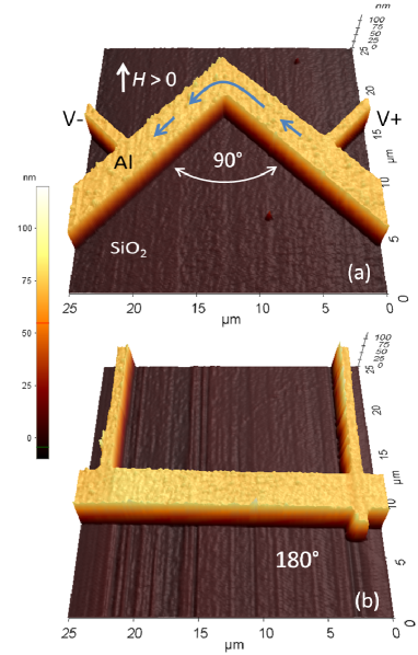
The samples investigated were all co-fabricated on the same chip and consist of electron-beam lithographically defined Al structures of thickness = 67 2 nm, deposited by rf sputtering on top of a Si/SiO2 substrate. We focus on two different geometries. Sample S90 consist of a 3.3 m wide transport bridge with a 90∘ corner equidistant from two voltage probes separated 9.6 m from the inner angle of the sharp bend. Similarly, S180 is a conventional straight transport bridge 3.7 m wide and with voltage probes separated by 20.9 m. These dimensions depart from the nominal values and were obtained via atomic force microscopy as shown in Figure 1(a)-(b).
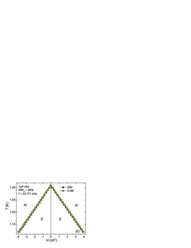
The field dependence of the superconducting-to-normal metal transitions, (), determined as 0.95, where is the normal state resistance, and using an ac-currentelectronics of 1 A, is basically the same for the two samples studied (see Figure 1(c)). This similarity of the phase boundaries allows us to make reliable and direct comparisons between the two samples without the necessity to work with reduced temperatures or field units. The critical temperature at zero field is K and the superconducting coherence length obtained from the Ginzburg-Landau approximation is nm. The BCS coherence length for Al of similar characteristics romijn ( and ) as the one used here is nm, indicating that our Al falls in the dirty limit , with the electronic mean free path. Using the relation we deduce nm. An independent estimation of nm can be obtained from the normal state resistivity m, and takingromijn m2. In the dirty limit the magnetic penetration depth is given by 145 nm, where 16 nm is the London penetration depth. For thin film geometry with a perpendicular external field we need to use the Pearl lengthpearl . In the considered samples for 1.19 K.
Let us now concentrate on the current-voltage characteristics, (), of the considered systems. At zero external field, the () curves and, in particular the critical current, , should be uniquely defined, irrespective of the direction of the applied current. This independence on the direction of the current persists at all fields for the S180 sample, but does not hold for the S90 sample. Indeed, on the one hand, the outer angle of the sharp corner has a larger surface nucleation critical field (a factor higher for the S90) when compared to the critical field at the inner cornerschweigert thus making the outer corner a point of enhanced superconductivityvictor . On the other hand, stream-lines of the applied current tend to conglomerate at the inner cornerhall , depleting the order parameter at that place. Notice that both effects, larger surface nucleation field and lower applied current density at the sharper corner, share the same origin in the impossibility of both, screening or applied currents, to reach the tip of the bend.
The fact that current crowding at the inner corner leads to local depletion of the superconducting order parameter implies automatically a reduction of the surface barrier for vortex penetrationclem-peeters as long as the applied current is such that the Lorentz force pushes vortices from the inner towards the outer corner. However, if the current is reversed, vortices will not penetrate from the outer corner (where total current is nearly zero) but rather symmetrically from the straight legs of the bridgeclem-peeters . As a consequence of this different nucleation position and nucleation condition for the two opposite current directions, it is predicted that such a simple corner shape wire will give rise to asymmetric () characteristics and therefore to a vortex ratchet effect.
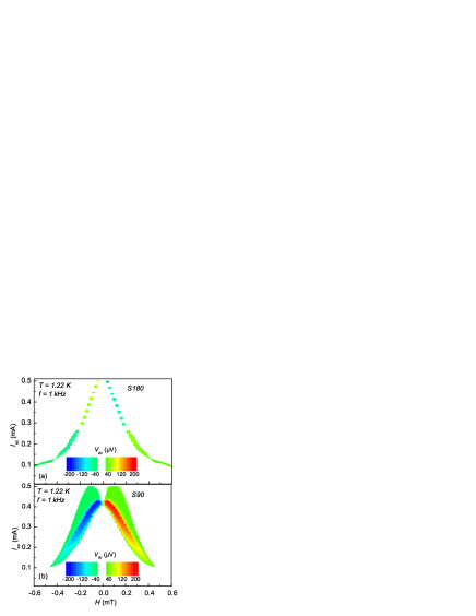
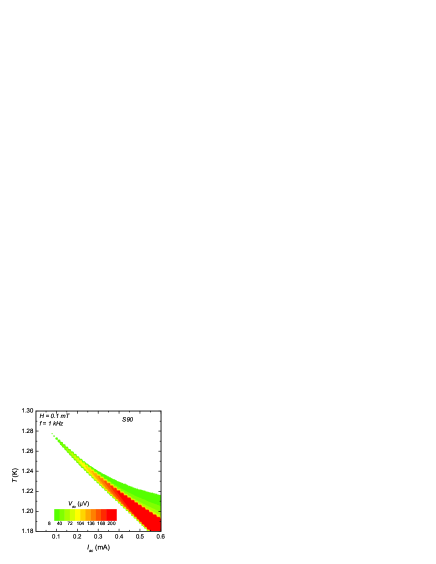
In order to demonstrate the existence of vortex motion rectification we submitted the samples to an ac current excitation of zero mean, , while measuring simultaneously the dc drop of voltage . The results of these measurements () are presented in Figure 2 for both samples. The chosen temperature K is such that m m m ensuring the existence of vortices within the superconductor. There are several points that deserve to be highlighted here, (i) rectification effects are almost completely absent in the S180 sample, (ii) there is a very strong ratchet signal for the S90 sample, (iii) the ratchet signal changes polarity at zero field. Ideally, we expect no ratchet effect at all from the S180 sample, however, the fact that both voltage contacts are on the same side of the strip already impose a weak asymmetry in the system which can lead to asymmetric vortex penetrationvodolazov-peeters ; cerbu . In any case, the rectification signal obtained in the S180 sample is negligible in comparison to that observed in the sample with the sharp turn. The fact that the rectification signal is positive at positive fields for the S90 sample, and according to the sign convention depicted in Fig. 1(a), we conclude that the easy direction of vortex flow is from the inner corner towards the outer corner, in agreement with the theoretical findings clem-peeters . In Fig.3 we show how the ratchet signal progressively disappears as the temperature approaches 1.280 K. For temperatures above this value vortices cannot fit anymore in the bridge and consequently the difference between the two corners vanishes. Similar ratchet effects due to surface barrier asymmetry, have been recently reportedkajino in high-Tc superconducting asymmetric nanobridges, with one side straight and the other having a constriction with an angle of 90∘.
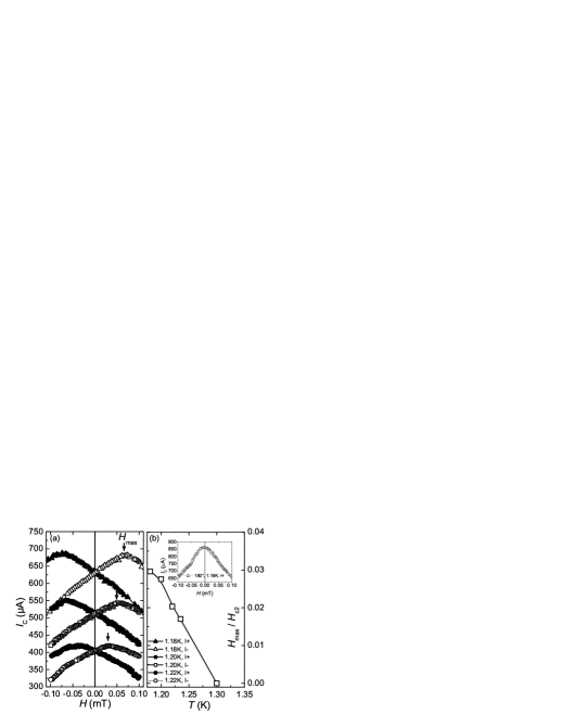
Notice that the ratchet effect here described results from the crowding of the applied current at the inner corner, and it would exist even if no screening currents were present. Let us now consider the additional effect of the screening currents. As it has been pointed out in Ref.[clem-peeters, ] based on both, London and Ginzburg-Landau theories, for a given direction of the applied current (as indicated in Fig.1(a)) a positive magnetic field will reinforce the total current (i.e. applied plus screening) at the inner corner and therefore the critical current will decrease as the field intensity increases. On the contrary, a negative applied magnetic field will induce a screening current which partially compensates the applied current at the inner corner and a field dependent increase of the critical current is expected clem-peeters . We have experimentally confirmed this prediction by measuring the critical current using a voltage criterion of 1 V as a function of field and current orientation. The results are presented in Figure 4(a) for three different temperatures and for the case where . For positive current and field (as defined in Fig.1(a)), we observe a monotonous decrease of . In contrast to that, for positive current and negative field, a clear enhancement of with field is observed for , whereas for a monotonous decrease of is recovered as a consequence of antivortices induced by the magnetic fieldclem-peeters that start to penetrate the sample. Reversing the applied current should lead to the opposite behavior, as indeed observed in Fig.4(a). This double test for all polarities of current and field also permits us to accurately determine the value of zero external field at the point where both curves cross each other. This has been convincingly confirmed by independent measurement of the remanent field in the S180 sample. For the sake of comparison, in the inset of Fig.4(b) we show the critical current for the S180 sample as a function of field. Notice that for this sample, the peak of maximum critical current is located at , in contrast to the behavior observed in sample S90. It is important to point out that in Ref.[13] the theoretical prediction of the curves in Fig.4(a) corresponds to a sharp inverted-V shape according to the London model, whereas the Ginzburg-Landau calculations yield a rounded top, which becomes sharper the smaller the ratio of to . This effect appears to be confirmed, at least qualitatively, in Fig. 4(a), in which the peaks become more rounded as the temperature increases and increases.
The compensation field is expected to depend on temperature since it is determined by the screening currents. In Fig.4(b) we plot the temperature dependence of where it can be noticed that this compensation field is a small fraction of the upper critical field in agreement with the theoretical calculationsclem-peeters .
To summarize, the superconducting properties of corner-shaped Al microstrips have been investigated. We show that sharp 90 degrees turns lead to asymmetric vortex penetration, being easier for vortices to penetrate from the inner side than from the outer side of the angle. We provide experimental confirmation of the predictedclem-peeters competing interplay of superconducting screening currents and applied currents at the inner side of the turn. We prove that current crowding leads to a distinctly different superconducting responses for positive and negative fields (or currents). These effects are evidenced also by a field dependent critical current enhancement and also by a strong rectification of the voltage signal, thus making these asymmetric superconducting nanocircuits efficient voltage rectifiers. Complementary measurements done in samples with 30∘ and 60∘ corners (not shown) reproduce the results presented here, i.e. ratchet signal and field-induced increase of critical current.
This work was partially supported by the Fonds de la Recherche Scientifique - FNRS, FRFC grant no. 2.4503.12, the Methusalem Funding of the Flemish Government, the Fund for Scientific Research-Flanders (FWO-Vlaanderen), the Brazilian funding agencies FAPESP and CNPq, and the program for scientific cooperation F.R.S.-FNRS-CNPq. J. V.d.V. acknowledges support from FWO-Vl. The authors acknowledge useful discussions with V. Gladilin.
References
- (1) K. K. Likharev, Rev. Mod. Phys. 51, 101 (1979)
- (2) M. Yu. Kupriyanov and V. F. Lukichev, Sov. J. Low Temp. Phys. 6, 210 (1980)
- (3) J. Romijn, T. M. Klapwijk, M. J. Renne, and J. E. Mooij, Phys. Rev. B 26, 3648 (1982)
- (4) J. Pearl, Appl. Phys. Lett. 5, 65 (1964)
- (5) see L. N. Bulaevskii, M. J. Graf, and V. G. Kogan, Phys. Rev. B 85, 014505 (2012) and references therein.
- (6) Notice that the nucleation of superconductivity itself is also influenced strongly by the presence of the corners, see, for example, GL treatment of this problem in a wedge in F. Brosens, V. M. Fomin, J. T. Devreese, V. V. Moshchalkov, Solid State Commun. 144, 494(2007) and in S.N. Klimin, V.M. Fomin, J.T. Devreese, V.V. Moshchalkov, Solid State Commun. 111, 589-593 (1999)
- (7) F. B. Hagedorn and P. M. Hall, J. Appl. Phys. 34, 128 (1963)
- (8) A. V. Silhanek, J. Van de Vondel, V. V. Moshchalkov, A. Leo, V. Metlushko, B. Ilic, V. R. Misko, and F. M. Peeters, Appl. Phys. Lett. 92, 176101 (2008)
- (9) J. R. Clem and K. K. Berggren, Phys. Rev. B 84, 174510 (2011)
- (10) H. L. Hortensius, E. F. C. Driessen, T. M. Klapwijk, K. K. Berggren, J. R. Clem, Appl. Phys. Lett. 100, 182602 (2012)
- (11) D. Henrich, P. Reichensperger, M. Hofherr, J. M. Meckbach, K. Ilâin, M. Siegel, A. Semenov, A. Zotova, D. Yu. Vodolazov, arXiv:1204.0616v2
- (12) J. I. Vestgarden and T.H. Johansen, Supercond. Sci. Technol. 25, 104001 (2012)
- (13) J. R. Clem, Y. Mawatari, G. R. Berdiyorov, F. M. Peeters, Phys. Rev. B 85, 144511 (2012)
- (14) The transport measurements have been done with the sample immersed in superfluid 4He for minimizing heating effects. Special care has been taken to avoid the high frequency noise signal (above 1 MHz ) by using a pi-filter.
- (15) V. A. Schweigert and F. M. Peeters, Phys. Rev. B 60, 3084 (1999)
- (16) D. Y. Vodolazov and F. M. Peeters, Phys. Rev. B 72, 172508 (2005)
- (17) D. Cerbu et al. unpublished
- (18) K. Kajino, K. Fujita, B. An, M. Inoue, A. Fujimaki, Jpn. J. Appl. Phys. 51, 053101 (2012)