Photo-thermal response in dual-gated bilayer graphene
Abstract
The photovoltaic and bolometric photoresponse in gapped bilayer graphene was investigated by optical and transport measurements. A pulse coincidence technique at 1.5 m was used to measure the response times as a function of temperature. The bolometric and photovoltaic response times were found to be identical implying that the photovoltaic response is also governed by hot electron thermal relaxation. Response times of 100 - 20 ps were found for temperatures from 3 - 100 K. Above 10 K, the relaxation time was observed to be = 25 5 ps, independent of temperature within noise.
pacs:
78.67.Wj, 78.47.D-, 78.56.-aThere is growing recognition that graphene has exceptional potential as a new optoelectronic material, which has led to a flurry of recent research activity and rapid advances. Avouris2009 ; Avouris2010 ; Novoselov2011 Graphene’s unique massless band structure gives rise to direct transitions and strong (specific) coupling to light at all wavelengths, CastroNeto2009 and ultra-fast response (from nanosecond to femtosecond) CastroNeto2009 room temperature operation for many applications. A photovoltaic response has been observed for visible light and we have recently observed both photovoltaic and bolometric response in bilayer graphene at THz frequencies. Jun_Kim2012 Diode-like rectification behavior is observed with contacts to dissimilar metals. GoldhaberGordon2008 ; Avouris2009 ; Avouris2010 ; Jun_Kim2012 However, the mechanism of the photovoltaic response has not been definitively identified. Both p-n junction physics similar to conventional semiconductor photovoltaic sensors and a thermoelectric mechanism remain viable possibilities. In a recent study we observed a hot electron bolometric response in bilayer graphene, which highlighted the outstanding thermal properties of graphene. Jun_Kim2012 Therefore, understanding the role of hot electron effects in the photoresponse of graphene is critical to the development of graphene-based optoelectronic devices such as bolometers and photovoltaic sensors. Gabor2011
Excited electrons in graphene thermalize quickly on the femtosecond time scales Rana2008 ; Heinz2010 by electron-electron scattering. DasSarma2008 These hot electrons transfer their thermal energy to the graphene lattice by the emission of phonons on a much longer time scale because of the weak electron-phonon interaction. DasSarma2008 ; Fuhrer2008 ; MacDonald2009 ; Viljas2010 The thermal relaxation of hot electrons by optical phonons Rana2011 ; Heinz2010 ; SunXu2012 and by acoustic phonons Jun_Kim2012 ; McEuen2012 has received much recent attention. The processes of cooling by optical and acoustic phonons are clearly distinguishable because their thermal timescales differ by a few orders of magnitude. High pulse energy radiation produces hot electrons with energies above the optical phonon energy ( 200 meV) that cool by optical phonon emission in a timescale of a few picoseconds. Rana2011 ; Heinz2010 ; SunXu2012 For longer times and/or lower pulse energy radiation, acoustic phonon assisted cooling is dominant with sub-nanosecond timescales. Jun_Kim2012 ; McEuen2012
Hot electrons can be utilized for bolometric and photovoltaic photoresponse detection. Jun_Kim2012 ; Levitov2011 ; Gabor2011 The bolometric response makes use of the temperature dependence of the resistivity, which is significant in gapped bilayer graphene. On the other hand, the hot electrons can also give rise to a photo-thermoelectric response. Diffusion of heat and carriers to the contacts produce a thermoelectric response. A competing mechanism for photovoltaic response is charge separation by the built-in electric fields at metal-graphene junctions due to proximity doping. It remains unclear which of these two mechanisms dominates in graphene photovoltaic devices.
In this paper, we use electrical transport and optical photoresponse measurements to characterize the bolometric and photovoltaic response of a dual-gated bilayer graphene device. The temperature-dependent resistance of the device which allows a bolometric response is characterized both optically and with AC transport measurements, which together establish that the response is thermal. We found that light also generates a voltage across the sample with zero bias current. We compare this photovoltaic response with the well-understood bolometric signal in the same device as functions of dual-gate voltages and temperature. In particular pulse coincidence measurement reveals that the photo voltage displays the same temperature-dependent relaxation time as the bolometric response, demonstrating that diffusive hot carrier relaxation in graphene dominates the observed photo voltage of the device.
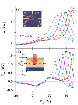
The bilayer graphene device we studied was fabricated by mechanical exfoliation of natural graphite on a resistive silicon wafer (200 cm) which was ion implanted with boron and annealed to provide a highly conducting but transparent back-gate at cryogenic temperatures. A 300 nm thick SiO2 layer was grown by a dry oxidation process from the silicon wafer. A micrograph of the device is shown in Fig. 1(a) inset and schematic of device geometry is shown in Fig. 1(b) inset. A thin Nichrome film was used as a semitransparent top-gate. Details of the device structure and the gating scheme can be found in Ref. Jun_Kim2012, . The dual-gated structure allows for independent tuning of carrier density and bandgap of the bilayer graphene device. Figure 1(a) shows the device resistance at 7.3 K as a function of back gate voltage at various top gate voltages . A broad resistance peak appears near = 10 V independent of and is attributed to the part of the bilayer device that is not gated by the top gate. Jun2010 The other sharper peak shifts with and is attributed to dual-gated device region.
The photoresponse and sample resistance were measured simultaneously. The photoresponse shown in Fig. 1(b) was measured with bias current = 0 which gives the photovoltaic response . At = 10 V where the broad peak of occurs, also doesn’t depend on , and crosses zero at 15 V. This behavior is similar to that observed in photo-thermoelectric results reported in graphene. McEuen2010 ; Gabor2011 ; SunXu2012 For 20V, depends on both and , and reaches a maximum value at the maximum .
To measure the response times of these signals we used a pulse coincidence technique. The photoresponse was studied at 1.56 m with a pulsed laser with a 65-fs pulse width and 100 MHz repetition rate. Pulses from two fiber lasers are locked together with a tunable time separation at repetition rate near 100 MHz (Menlo Systems), which allows pulse coincidence measurements with precise time delays from a few ps to 10 ns without a mechanical delay line. The absorption of 1.56 m radiation in the graphene was estimated to be 1.2% by considering effects due to the silicon substrate and the Nichrome top gate. Jun_Kim2012 The graphene absorbs an average power of 0.37 nW from the pump and probe pulses and generates a temperature rise , which can be measured using the temperature dependence of .
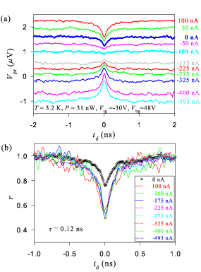
The dependence of the photoresponse with pulse time delay for different bias currents is shown in Fig. 2(a) under conditions that the device is gated to its charge neutral point. At zero bias current the signal is purely photovoltaic. For non-zero bias there is also a bolometric signal given by which was reported earlier. Jun_Kim2012 We find that the total photoresponse can be described as allowing a separation of the photovoltaic and bolometric contributions. Therefore the bolometric response can be obtained from . It is seen in the figure that this bolometric response is dominant except near where the response is purely photovoltaic.
These pulse time delay data allow a measurement of the response time of the two components of the photoresponse. For long pulse delay times, , average probe-pulse induced photo voltage, does not change with respect to the time delay . When the delay is short (), however, the magnitude of is reduced due to the nonlinear radiation power dependence of the response so that the photo voltage displays a peak or dip at . The magnitude of this peak or dip increases with the non-linear power dependence of .
Figure 2(b) shows and normalized to the response in the absence of the pump pulse for several different . All of the normalized for different collapse to one curve because the small Joule heating does not significantly raise the electron temperature above the lattice temperature. Both bolometric and photovoltaic responses produce a narrow dip with a sub-nanosecond width at zero time delay when the pump and probe pulses are coincident. Surprisingly, the widths of both bolometric and photovoltaic dips are seen to be the same to within the experimental error. The time constants determined by the half widths at half maximum of the dips are ns. This demonstrates that both and have the same response time and since the bolometric response is clearly thermal Jun_Kim2012 this implies that the photovoltaic response is also thermal. Similar results are observed at V and V for temperatures below 10 K.
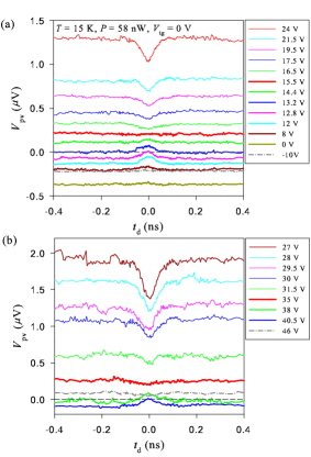
To gain further insight into the nature of the photo voltage, we measured its gate voltage dependence. Figure 3 shows back gate voltage dependence of photo voltage at K with 0 and 0. As can be seen from the data in Fig. 1(a), the top gate does not gate the entire device. To obtain uniform gating we control only the back gate voltage with zero top gate voltage. Figures 3(a) and (b) display the photovoltaic response below and above the maximum observed at around V. The peak or dip structure is associated with the sign of , and its depth or height depends on the nonlinear power dependence of . Both sign and power nonlinearity depend on back gate voltage. For example, at V the response is independent of indicating that is linear with radiation power. As the power nonlinearity of grows above or below V, the dip or peak of appears and grows. Remarkably, however, all of the pump-probe data have the same ps ps. The gate-independent time constant shows that the photovoltaic response is thermal at all gate voltages not only at maximum with respect to as shown in Fig. 2(b) where it could be directly compared with the bolometric response. This observation demonstrates that the photovoltaic response time in bilayer graphene is the intrinsic thermal time constant of hot electron energy relaxation.
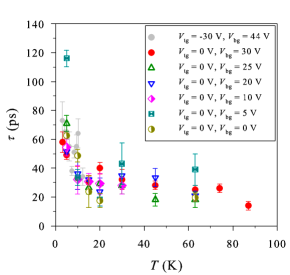
We also measured the temperature dependence of the response time in our graphene device. Figure 4 exhibits obtained from the photovoltaic response in the temperature range 3 K - 87 K at several different dual-gate voltages. The response time for different gate voltages coincides within error as shown in Fig. 4. The time constant decreases from 80 ps at 3 K to 20 ps at 80 K. Above 10 K, is seen to be temperature independent to within experimental error.
The thermal relaxation rate is given by the ratio of the electronic heat capacity to thermal conductance . The thermal conductance was obtained using transport measurements as described in Ref. Jun_Kim2012, . For K, the transport measurements gives nW/K which is in reasonable agreement with the value estimated for cooling by acoustic phonons. Viljas2010 A crossover of the thermal conductance from to linear is predicted for , where is the Bloch-Grünheisen temperature given by . Viljas2010 Assuming a sound velocity m/s Efetov2010 and a disorder-induced charge density of cm-2 Yan2008 , we find K. Although our sample is nominally charge neutral at , it is widely accepted that disorder creates electron-hole puddles Martin2008 and thus is non-zero at all gate voltages. Transport measurements show that the Bloch-Grünheisen regime behavior occurs for K. Efetov2010 The behavior of and above may be complicated by disorder induced supercollision cooling McEuen2012 ; Levitov2012 and/or the non-parabolic band structure of gapped bilayer graphene CastroNeto2009 which leads to small Fermi energies. We measured nW/K for K, which is reasonable in view of these considerations.
On the other hand, diffusion cooling of hot electrons also gives a linear dependent thermal conductance. Diffusion cooling provides a thermal conductance , by the Wiedermann-Franz law, where nW/K2 is the Lorentz number, and is bilayer graphene resistance. At the peak resistance for our sample, W/K, which is two orders of magnitude smaller than the electron-phonon conductance. We conclude that acoustic phonon mediated cooling of hot electrons is dominant in our samples.
We note, however, that the thermoelectric and photovoltaic signals are a consequence of diffusion. For asymmetric contacts the thermal diffusion and charge flow at the two contacts differs leading to a net potential difference. The diffusion length is estimated to be 0.5 m at 10 K which is much smaller than the sample size of 5 m so that the sample temperature rise and response time is dominated by the thermal conductance to the lattice which greatly reduces the thermoelectric signals in these large area, low conductance samples. The thermoelectric effect produces an electric field , where is the Seebeck coefficient and is the gradient of the temperature. The heat conductance to the lattice diminishes at the contact and therefore the thermoelectric field by a factor of compared with pure diffusion.
At low temperatures (, where is the local Fermi energy in the graphene and is the Boltzmann constant) the electronic specific heat is , where , where is the density of states for bilayer graphene. In the parabolic band approximation of (ungapped) graphene where the interlayer coupling meV Zhang2008 , m/s is the monolayer graphene Fermi velocity. For our sample area of 25 , this gives J/K2. Thus the thermal response time of our bilayer sample can be estimated ps independent of temperature for K which is in reasonable agreement with the measured shown in Fig. 4.
In summary, we have reported photovoltaic response time measurements on gapped bilayer graphene. The devices show both bolometric and photovoltaic responses, which were separated by their bias current dependence. The identical response time constants observed for the bolometric and photovoltaic responses as a function of gate voltages and temperature implies that both effects are governed by the same intrinsic hot electron-phonon thermal relaxation process. The observed response times of 10 - 100 ps indicates that hot electron relaxation occurs through acoustic phonon emission. These observations support the growing realization that graphene appears to have great promise for fast sensitive photo detectors over a wide spectral range.
Acknowledgements.
The authors thank A. B. Sushkov, G. S. Jenkins, and D. C. Schmadel for helping with the optical cryostat setup and for valuable discussions. This work was supported by IARPA, the ONR MURI program and the NSF (grants DMR-0804976 and DMR-1105224) and in part by the NSF MRSEC (grant DMR-0520471).References
- (1) F. Xia, T. Mueller, Y.-M. Lin, A. Valdes-Garcia, and P. Avouris, Nature Nanotech. 4, 839 (2009).
- (2) T. Mueller, F. Xia, and P. Avouris, Nature Photonics 4, 297 (2010).
- (3) T. J. Echtermeyer, L. Britnell, P. K. Jasnos, A. Lombardo, R. V. Gorbachev, A. N. Grigorenko, A. K. Geim, A. C. Ferrari, and K. S. Novoselov, Nature Commun. 2, 458 (2011).
- (4) A. H. Castro Neto, F. Guinea, N. M. R. Peres, K. S. Novoselov, and A. K. Geim, Rev. Mod. Phys. 81, 109 (2009).
- (5) J. Yan, M.-H. Kim, J. A. Elle, A. B. Sushkov, G. S. Jenkins, H. M. Milchberg, M. S. Fuhrer, and H. D. Drew, Nature Nanotech. 7, 472 (2012).
- (6) B. Huard, N. Stander, J. A. Sulpizio, and D. Goldhaber- Gordon, Phys. Rev. B 78, 121402 (2008).
- (7) N. M. Gabor, J. C. W. Song, Q. Ma, N. L. Nair, T. Taychatanapat, K. Watanabe, T. Taniquchi, L. S. Levitov, 5 and P. Jarillo-Herrero, Science 334, 648 (2011).
- (8) P. A. George, J. Strait, J. Dawlaty, S. Shivaraman, M. Chandrashekhar, F. Rana, and M. G. Spencer, Nano Lett. 8, 4248 (2008).
- (9) C. H. Lui, K. F. Mak, J. Shan, and T. F. Heinz, Phys. Rev. Lett. 105, 127404 (2010).
- (10) W.-K. Tse, E. H. Hwang, and S. D. Sarma, Appl. Phys. Lett. 93, 023128 (2008).
- (11) J.-H. Chen, C. Jang, S. Xiao, M. Ishigami, and M. S. Fuhrer, Nature Nanotech. 3, 206 (2008).
- (12) R. Bistritzer and A. H.MacDonald, Phys. Rev. Lett. 102, 206410 (2009).
- (13) J. K. Viljas and T. T. Heikkilä, Phys. Rev. B 81, 245404 (2010).
- (14) J. H. Strait, H. Wang, S. Shivaraman, V. Shields, M. Spencer, and F. Rana, Nano Lett. 11, 4902 (2011).
- (15) D. Sun, G. Aivazian, A. M. Jones, J. S. Ross, W. Yao, D. Cobden, and X. Xu, Nature Nanotech. 7, 114 (2012).
- (16) M. W. Graham, S.-F. Shi, D. C. Ralph, J. Park, and P. L. McEuen, Nature Phys. AOP (2012), DOI:10.1038/nphys2493.
- (17) J. C. W. Song, M. S. Rudner, C. M. Marcus, and L. S. Levitov, Nano Lett. 11, 4688 (2011).
- (18) J. Yan and M. S. Fuhrer, Nano Lett. 10, 4521 (2010).
- (19) X. Xu, N. M. Gabor, J. S. Alden, A. M. van der Zande, and P. L. McEuen, Nano Lett. 10, 562 (2010).
- (20) D. K. Efetov and P. Kim, Phys. Rev. Lett. 105, 256805 (2010).
- (21) J. Yan, E. A. Henriksen, P. Kim, and A. Pinczuk, Phys. Rev. Lett. 101, 136804 (2008).
- (22) J. Martin, N. Akerman, G. Ulbricht, T. Lohmann, J. H. Smet, K. von Klitzing, and A. Yacoby, Nature Phys. 4, 144 (2008).
- (23) J. C. W. Song, M. Y. Reizer, and L. S. Levitov, Phys. Rev. Lett. 109, 106602 (2012).
- (24) L. M. Zhang, Z. Q. Li, D. N. Basov, M. M. Fogler, Z. Hao, and M. C. Martin, Phys. Rev. B 78, 235408 (2008).