Second harmonic microscopy of monolayer MoS2
Abstract
We show that the lack of inversion symmetry in monolayer MoS2 allows strong optical second harmonic generation. Second harmonic of an 810-nm pulse is generated in a mechanically exfoliated monolayer, with a nonlinear susceptibility on the order of 10-7 m/V. The susceptibility reduces by a factor of seven in trilayers, and by about two orders of magnitude in even layers. A proof-of-principle second harmonic microscopy measurement is performed on samples grown by chemical vapor deposition, which illustrates potential applications of this effect in fast and non-invasive detection of crystalline orientation, thickness uniformity, layer stacking, and single-crystal domain size of atomically thin films of MoS2 and similar materials.
Recently, there is a growing interest in exploring new types of atomically thin crystals based on layered materials, such as transition metal dichalcogenides.Wang et al. (2012a) The most extensively studied member of this family is MoS2. In 2010, photoluminescence experimentsMak et al. (2010); Splendiani et al. (2010) and microscopic calculationsKuc et al. (2011); Splendiani et al. (2010) indicated that, although bulk MoS2 is an indirect semiconductors, its monolayer is a direct semiconductor with a bandgap of about 1.88 eV. Such a large bandgap and the structural similarity with widely studied graphene immediately stimulated investigations on its potential applications in logic electronics.Liu et al. (2011); Yoon et al. (2011) In 2011, top-gated transistors based on MoS2 monolayers were fabricated.Radisavljevic et al. (2011a) Later, integrated circuits based on monolayerRadisavljevic et al. (2011b) and bilayerWang et al. (2012b) for logic operations were demonstrated. Ambipolar transport in a multilayer transistor gated by ionic liquids was also demonstrated, showing the feasibility to develop p-n-junction-based devices.Zhang et al. (2012) Furthermore, the recently demonstrated superior strength and flexibilityBertolazzi et al. (2011) make MoS2 atomic layers an attractive candidate for applications in flexible electronics.He et al. (2012); Pu et al. (2012) In addition, since monolayer MoS2 has a bandgap in the visible range, has workfunctions that are compatible with commonly used electrode materials, and has stable charge exciton state even at room temperature,Mak et al. (2013) it is also an attractive candidate for various optoelectronic and photonic applications, such as phototransistorsYin et al. (2012); Lee et al. (2012a) and heterojunction solar cells.Shanmugam et al. (2012)
In contrast to these breakthroughs in understanding the mechanical, electronic, and linear optical properties of MoS2 atomic layers, little is known about their nonlinear optical properties. Nonlinear optical responses are important aspects of light-matter interaction, and can play important roles in various photonic and optoelectronic applications, especially in those involving high intensity laser beams. Bulk MoS2 crystal with stacking order belongs to space group , which is inversion symmetric. Hence, its second-order nonlinear response should vanish.Boyd (2008) Indeed, one early experiment showed that second-order nonlinear susceptibility of bulk MoS2 is at most 10-14 m/V.Wagoner et al. (1998) However, the inversion symmetry is broken in a monolayer, which has symmetry. One consequence of such a symmetry reduction is to allow valley-selective optical interband transitions, which has been observed by several groups recentlyCao et al. (2012); Zeng et al. (2012); Mak et al. (2012); Xiao et al. (2012); Sallen et al. (2012); Mak et al. (2013) and can be used for valleytronics, in which the valley index of electrons is used to carry information. Here we show that the lack of inversion symmetry allows unusually strong optical second harmonic generation (SHG) in monolayer MoS2 flakes prepared by mechanical exfoliation and chemical vapor deposition (CVD). This effect is very sensitive to layer thickness, crystalline orientation, and layer stacking. Based on these properties, we demonstrate a second harmonic microscopy for characterization of MoS2 thin films.
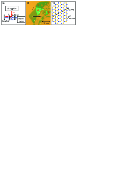
Figure 1(a) shows the experimental setup. The fundamental pulse with an angular frequency and a central wavelength of 810 nm is obtained from a Ti:sapphire laser. It is tightly focused to a spot of 2 m (full width at half maximum) by a microscope objective lens. The second harmonic (SH) generated is collected by the same lens, and detected by a spectrometer equipped with a thermoelectric cooled silicon charge-coupled device camera. A set of color filters is used to block the fundamental and other unwanted light. With 810-nm wavelength, band-to-band absorption of fundamental is avoided, and both fundamental and SH can be detected efficiently with silicon detectors, which facilitates alignment and location of the laser spot. Figure 1(b) is a microscope photo of a MoS2 flake that is mechanically exfoliated onto a Si/SiO2 (90 nm) substrate. The region marked with red label 1L is identified as a monolayer according to its optical contrast,Benameur et al. (2011); Li et al. (2012); Castellanos-Gomez et al. (2010) Raman spectrum,Lee et al. (2010); Molina-Sanchez and Wirtz (2011) and photoluminesence spectrum.Mak et al. (2010); Splendiani et al. (2010) Other regions with few atomic layers, as indicated by the red labels, are assigned according to their relative optical contrasts.
The structure of monolayer MoS2 is schematically shown in Fig. 1(c), where each yellow circle represents two S atoms vertically separated by 0.65 nm, and blue circles indicate plane of Mo atoms located between the two S atomic planes. With the symmetry, the second-order nonlinear susceptibility tensor has nonzero elements of ,Boyd (2008) where are crystalline coordinates. Here, is along the armchair direction, which is from the zig-zag direction, along which the mirror symmetry is broken. In the experiment, the fundamental beam is normal incident (along ) and is linearly polarized along horizontal direction [defined as in the laboratory coordinates, as shown in Fig. 1(b)]. It is straightforward to show that the parallel () and perpendicular () components of SH field are proportional to and , respectively, where is the angle between and . Hence, the power of the two components varies as and , while the total power is independent of .
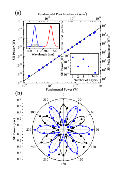
In our experiment, we first measure the total SH power with a fundamental power of 4 mW. The upper inset of Fig. 2(a) shows the spectra of the SH (blue) and the fundamental (red), confirming that the former is indeed at half wavelength of the latter. The gray curve is a spectrum (multiplied by a factor of 100) taken under the same conditions but with the laser spot located on bare substrate. Hence, the contrast of monolayer with respect to substrate is at least 104, which is much higher than linear optical microscopy (about 0.3). The main panel of Fig. 2(a) shows how the SH power varies with the fundamental power. The peak irradiance of fundamental and SH pulses, deduced from the powers, are also plotted for convenience, as top and right axes. The solid line is the expected quadratic dependence for the SHG process. Next, by placing a linear polarizer in front of the spectrometer, we measure and as a function of , the angle between and , by rotating the sample about axis. Figure 2(b) shows the results, along with the expected dependence (solid lines) from the symmetry.
In order to estimate the magnitude of from the measurement, we model the monolayer as a bulk medium. Since the flake thickness ( nm) is much smaller than the coherence length, the SHG is not influenced by phase-matching conditions. By solving the coupled-wave equations,Boyd (2008) the SH field amplitude of the parallel component
| (1) |
where is the speed of light in a vacuum and is the index of refraction at SH, and is the fundamental field amplitude. The is related to the irradiance by , which can be calculated from the measured quantity, average power, by considering that is Gaussian in both time and space, with widths (full width at half maxima) of and , respectively. By using = 2 m, = 200 fs, = 81 MHz, ,Castellanos-Gomez et al. (2010) and reflection coefficient of 0.09 from this multilayer structure, we find that the magnitude of is about m/V. We note that due to the nonlinear nature of this process, such a deduction replies on accurate knowledge on many experimental parameters, such as the shape and duration of the fundamental pulse, the shape and size of the focused fundamental spot at sample, and the relation between the measured spectral counts and the actually SH power. Hence, this value should be viewed as an order-of-magnitude estimate. However, the relative comparison of throughout this paper are not influenced by such uncertainties, and are thus accurate.
Since monolayer MoS2 possesses such a large , which vanishes in bulk, it is interesting to study how varies with the number of atomic layers. We measure the total power of SH from different regions of the flake shown in Fig. 1(b), with a fixed fundamental power of 4 mW. The results are summaries in the lower inset of Fig. 2(a). Since the total power is independent of , the measurement is not influenced by potentially different crystal orientations of these regions. We find that of trilayer is about a factor of seven smaller than monolayer, while those of bilayer and quadralayer are about two orders of magnitude smaller than the monolayer. Since flakes with even number of atomic layers possess inversion symmetry, their second-order response should vanish. The smaller but nonzero can be attributed to surface and interface effects. According to this measurement, the contrast of monolayer with respect to bilayer and quaralayer is about 104. Similar layer-number dependence has also been observed recently in WS2 and WSe2.Zeng et al. (2012) We also measure a thick flake that can be considered as a bulk. The SH power is about five orders of magnitude smaller than the monolayer, indicating a very small , as a result of the inversion symmetry.
The observed SHG can be used to fast and in-situ characterize atomically thin films of MoS2 and similar materials. Although high quality monolayer MoS2 can be produced by simple mechanical exfoliationNovoselov et al. (2005) and identified by optical contrast with certain substratesBenameur et al. (2011); Li et al. (2012) and Raman spectroscopy,Lee et al. (2010); Molina-Sanchez and Wirtz (2011) applications of this material rely on development of scalable techniques. Following initial works of mechanical exfoliation, other top-down methods with better potential for large-scale production have been developed, such as lithium ion exfoliationEda et al. (2011); Zeng et al. (2011); Dines (1975); Frey et al. (2003); Zeng et al. (2012) and ultrasonic exfoliation in liquids.Coleman et al. (2011); Smith et al. (2011); May et al. (2012); Zhou et al. (2011); Cunningham et al. (2012); Altavilla et al. (2011); O’neill et al. (2012) Promising progresses have also been made in developing bottom-up methods, including hydrothermal synthesisPeng et al. (2001a, b) and CVD on insulating substratesLee et al. (2012b); Zhan et al. (2012); Liu et al. (2012); Balendhran et al. (2012) and graphene.Shi et al. (2012) However, one significant obstacle is the lack of techniques for fast and in-situ sample characterization. For example, thin films of MoS2 fabricated by these techniques are polycrystalline. They are composed of single-crystalline domains with random crystal orientations and are separated by grain boundaries, which severely limit performance of the films, especially their conductivity and mechanical strength. However, it is difficult to locate the grain boundaries and monitor size of these domains in-situ.
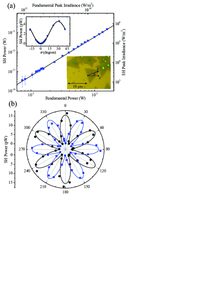
The lower inset of Fig. 3(a) shows a microscope photo of some triangular monolayer MoS2 flakes on a Si/SiO2(280 nm) substrate fabricated by CVD. The samples were prepared using MoO3 and sublimated sulfur as precursors. MoO3 is positioned close to the designated growth substrate at the center of the furnace, while sublimated sulfur is positioned upstream at a zone where evaporation starts at 750∘C. The reaction of the precursors at 850∘C in a furnace flushed with nitrogen results in nucleation of single crystalline domains. The density of nucleation and samples sizes can be controlled by monitoring the pressure and the closely related sulfur concentration in the chamber. By maintaining a positive pressure in the range of 5 - 20 KPa, MoS2 domains with sizes in the range of 10 - 40 m are synthesized, with a ramping time of 60 to 90 minutes and 10 minutes at the reaction temperature.Najmaei et al. (2013)
The main panel of Fig. 3(a) shows the quadratic power dependence of SHG, similar to Fig. 2(a), measured from the well-separated flake on which the crystalline and laboratory coordinates ( and , respectively) are plotted [the lower inset of Fig. 3(a)]. By rotating the sample, we measure and as a function of , as shown in Fig. 3(b). The results are similar to the exfoliated sample shown in Fig. 2(b). A separate measurement of the parallel component with finer resolution near , shown in the upper inset of Fig. 3(a), confirms that the minimal parallel component occurs precisely at . The edges of these triangular flakes are expected to be along zig-zag directions since these are lowest energy configurations.Lauritsen et al. (2007); Byskov et al. (2000) The maximum parallel component of SH should occurs when the fundamental is polarized along the zig-zag direction, which is consistent our observation. Hence, the SHG further confirms that the direction of the edges is zig-zag. We repeat the measurement with several other similar triangular flakes, and obtained the same result. Such an established relation also allows us to determine the crystal orientation of the mechanically exfoliated sample shown in Fig. 1(b): that is, the armchair direction of the 1L region is horizontal, and its lattice orientation is as shown in Fig. 1(c). From the strength of the SH, we deduce a m/V, which is about a factor of 20 smaller than the mechanically exfoliated flake.
Figure 4 summarizes our proof-of-principle demonstration of a polarization-revolved SH microscopy. We study a region on the substrate with quasi-continuos films, as shown in Fig. 4(a). It contains a high density but still separated and randomly oriented triangular flakes, so that we can correlate domains observed in SHG to the actual regions. In this measurement, we scan a 20-mW fundamental spot across the region indicated by the box in Fig. 4(a), and detect the powers of the parallel and perpendicular components of the SH, as shown in Figs. 4(b) and (c), respectively. The errors in these scans are below 2 pW, or smaller than 1% of the maximum signal. Figure 4(d) shows the total power, obtained by adding (b) and (c). From (b) and (c), we calculate the angle by using , as shown in (e). The uncertainty on the angle is below 1∘.
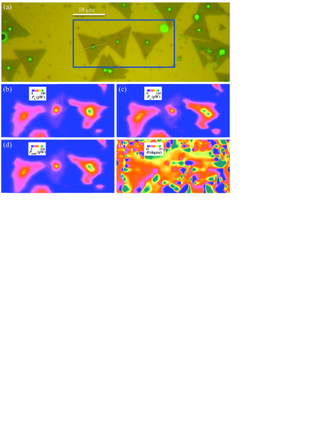
The combination of linear and nonlinear optical microscopy can provide valuable information on polycrystalline thin films grown by CVD. First, the greenish dots in Fig. 4(a) indicate that at the central area of some flakes, a second (or even third) layer is grown. Second harmonic images show that these areas have higher SH power. In bilayer MoS2 exfoliated from 2-stacked crystals, the two layers are inversely oriented so that the bilayer possesses inversion symmetry. Hence, it second-order response should vanish, as confirmed in Fig. 2(a). The higher SH power observed from multilayer regions of CVD-grown flakes indicates that these multilayers are not 2-stacked. This is similar to multilayer graphene grown by CVD. Clearly, the SH microscopy is capable of probing relative orientations among multilayers of MoS2. Second, panel (e) shows that is uniform over the left flake, which is about . This is consistent with the shape observed in (a) (white dashed line). With further growth time, this flake will merge with other flakes to form a continuous polycrystalline film. Linear optical microscopy would not allow identification of each single-crystalline domains. However the map can still distinguish these domains, locate their boundaries, and measure their sizes. Third, the shapes of these flakes are irregular in the SH maps. Especially, the parallel and perpendicular components have different edge shapes. This can be attributed to the roughness on the edges and different termination configurations on the edges. Although further characterizations are needed to correlate the microscopic structure on the edges to the SH power, this observation illustrates the potential of using SHG to study these edge structures. Finally, although the three flakes look similar in (a), the SH power are different, and the of the middle and right flakes are irregular. This illustrates that the SH microscopy can show different properties and qualities of the flakes that the linear optical microscopy cannot. However, further studies are needed to correlate SHG to these specific sample characteristics.
In summary, we have observed strong second harmonic generation in monolayer MoS2 fabricated by mechanical exfoliation and CVD, and performed a proof-of-principle second harmonic microscopy measurement. Our results show that such a nonlinear optical effect can be used to fast and non-invasively characterize atomically thin films of MoS2 and other similar materials. Compared to linear optical microscopy, the contrast is enhanced by at least four orders of magnitude. Unlike linear optical microscopy that replies on light interference from carefully designed multilayer substrates, such a nonlinear optical microscopy can be applied to any substrates with weak second-order nonlinearity, such as silicon and glass. Although Raman microscopy has also been used to identify monolayer MoS2, the Raman shift often depends on substrates, and the contrast is relatively low. In addition to these advantages in identifying monolayers, the second harmonic microscopy can probe crystal orientation, single-crystal domain size, and layer stacking.
HZ acknowledges support from the US National Science Foundation under Awards No. DMR-0954486 and No. EPS-0903806, and matching support from the State of Kansas through Kansas Technology Enterprise Corporation. JL acknowledges support from Welch Foundation (C-1716).
References
- Wang et al. (2012a) Q. H. Wang, K. Kalantar-Zadeh, A. Kis, J. N. Coleman, and M. S. Strano, Nat. Nanotechnol. 7, 699 (2012a).
- Mak et al. (2010) K. F. Mak, C. Lee, J. Hone, J. Shan, and T. F. Heinz, Phys. Rev. Lett. 105, 136805 (2010).
- Splendiani et al. (2010) A. Splendiani, L. Sun, Y. Zhang, T. Li, J. Kim, C. Y. Chim, G. Galli, and F. Wang, Nano Lett. 10, 1271 (2010).
- Kuc et al. (2011) A. Kuc, N. Zibouche, and T. Heine, Phys. Rev. B 83, 245213 (2011).
- Liu et al. (2011) L. Liu, S. B. Kumar, Y. Ouyang, and J. Guo, IEEE Trans. on Electron Devices 58, 3042 (2011).
- Yoon et al. (2011) Y. Yoon, K. Ganapathi, and S. Salahuddin, Nano Lett. 11, 3768 (2011).
- Radisavljevic et al. (2011a) B. Radisavljevic, A. Radenovic, J. Brivio, V. Giacometti, and A. Kis, Nat. Nanotechnol. 6, 147 (2011a).
- Radisavljevic et al. (2011b) B. Radisavljevic, M. B. Whitwick, and A. Kis, ACS Nano 5, 9934 (2011b).
- Wang et al. (2012b) H. Wang, L. L. Yu, Y. H. Lee, Y. M. Shi, A. Hsu, M. L. Chin, L. J. Li, M. Dubey, J. Kong, and T. Palacios, Nano Lett. 12, 4674 (2012b).
- Zhang et al. (2012) Y. Zhang, J. Ye, Y. Matsuhashi, and Y. Iwasa, Nano Lett. 12, 1136 (2012).
- Bertolazzi et al. (2011) S. Bertolazzi, J. Brivio, and A. Kis, ACS Nano 5, 9703 (2011).
- He et al. (2012) Q. Y. He, Z. Y. Zeng, Z. Y. Yin, H. Li, S. X. Wu, X. Huang, and H. Zhang, Small 8, 2994 (2012).
- Pu et al. (2012) J. Pu, Y. Yomogida, K. K. Liu, L. J. Li, Y. Iwasa, and T. Takenobu, Nano Lett. 12, 4013 (2012).
- Mak et al. (2013) K. F. Mak, K. He, C. Lee, G. H. Lee, J. Hone, T. F. Heinz, and J. Shan, Nat. Mater. 12, 207 (2013).
- Yin et al. (2012) Z. Yin, H. Li, H. Li, L. Jiang, Y. Shi, Y. Sun, G. Lu, Q. Zhang, X. Chen, and H. Zhang, ACS Nano 6, 74 (2012).
- Lee et al. (2012a) H. S. Lee, S. W. Min, Y. G. Chang, M. K. Park, T. Nam, H. Kim, J. H. Kim, S. Ryu, and S. Im, Nano Lett. 12, 3695 (2012a).
- Shanmugam et al. (2012) M. Shanmugam, T. Bansal, C. A. Durcan, and B. Yu, Appl. Phys. Lett. 100, 153901 (2012).
- Boyd (2008) R. W. Boyd, Nonlinear Optics, 3rd ed. (Academy Press, San Diego, USA, 2008).
- Wagoner et al. (1998) G. A. Wagoner, P. D. Persans, E. A. Van Wagenen, and G. M. Korenowski, J. Opt. Soc. Am. B 15, 1017 (1998).
- Cao et al. (2012) T. Cao, G. Wang, W. Han, H. Ye, C. Zhu, J. Shi, Q. Niu, P. Tan, E. Wang, B. Liu, and J. Feng, Nat. Commun. 3, 887 (2012).
- Zeng et al. (2012) H. Zeng, J. Dai, W. Yao, D. Xiao, and X. Cui, Nat. Nano. 7, 490 (2012).
- Mak et al. (2012) K. F. Mak, K. He, J. Shan, and T. F. Heinz, Nat. Nano. 7, 490 (2012).
- Xiao et al. (2012) D. Xiao, G. B. Liu, W. Feng, X. Xu, and W. Yao, Phys. Rev. Lett. 108, 196802 (2012).
- Sallen et al. (2012) G. Sallen, L. Bouet, X. Marie, G. Wang, C. R. Zhu, W. P. Han, Y. Lu, P. H. Tan, T. Amand, B. L. Liu, and B. Urbaszek, Phys. Rev. B 86, 081301 (2012).
- Benameur et al. (2011) M. M. Benameur, B. Radisavljevic, J. S. Hron, S. Sahoo, H. Berger, and A. Kis, Nanotechnology 22, 125706 (2011).
- Li et al. (2012) H. Li, G. Lu, Z. Y. Yin, Q. Y. He, H. Li, Q. Zhang, and H. Zhang, Small 8, 682 (2012).
- Castellanos-Gomez et al. (2010) A. Castellanos-Gomez, N. Agraït, and G. Rubio-Bollinger, Appl. Phys. Lett. 96, 213116 (2010).
- Lee et al. (2010) C. Lee, H. Yan, L. E. Brus, T. F. Heinz, J. Hone, and S. Ryu, ACS Nano 4, 2695 (2010).
- Molina-Sanchez and Wirtz (2011) A. Molina-Sanchez and L. Wirtz, Phys. Rev. B 84, 155413 (2011).
- Zeng et al. (2012) H. Zeng, G.-B. Liu, J. Dai, Y. Yan, B. Zhu, R. He, L. Xie, S. Xu, X. Chen, W. Yao, and X. Cui, ArXiv e-prints (2012), arXiv:1208.5864 .
- Novoselov et al. (2005) K. S. Novoselov, D. Jiang, F. Schedin, T. J. Booth, V. V. Khotkevich, S. V. Morozov, and A. K. Geim, Proc. Natl. Acad. Sci. U.S.A. 102, 10451 (2005).
- Eda et al. (2011) G. Eda, H. Yamaguchi, D. Voiry, T. Fujita, M. Chen, and M. Chhowalla, Nano Lett. 11, 5111 (2011).
- Zeng et al. (2011) Z. Zeng, Z. Yin, X. Huang, H. Li, Q. He, G. Lu, F. Boey, and H. Zhang, Angew. Chem. Int. Ed. 50, 11093 (2011).
- Dines (1975) M. B. Dines, Mater. Res. Bul. 10, 287 (1975).
- Frey et al. (2003) G. L. Frey, K. J. Reynolds, R. H. Friend, H. Cohen, and Y. Feldman, J. Am. Chem. Soc. 125, 5998 (2003).
- Zeng et al. (2012) Z. Zeng, T. Sun, J. Zhu, X. Huang, Z. Yin, G. Lu, Z. Fan, Q. Yan, H. H. Hng, and H. Zhang, Angew. Chem. Int. Ed. 51, 9052 (2012).
- Coleman et al. (2011) J. N. Coleman, M. Lotya, A. O’neill, S. D. Bergin, P. J. King, U. Khan, K. Young, A. Gaucher, S. De, R. J. Smith, I. V. Shvets, S. K. Arora, G. Stanton, H.-Y. Kim, K. Lee, G. T. Kim, G. S. Duesberg, T. Hallam, J. J. Boland, J. J. Wang, J. F. Donegan, J. C. Grunlan, G. Moriarty, A. Shmeliov, R. J. Nicholls, J. M. Perkins, E. M. Grieveson, K. Theuwissen, D. W. McComb, P. D. Nellist, and V. Nicolosi, Science 331, 568 (2011).
- Smith et al. (2011) R. J. Smith, P. J. King, M. Lotya, C. Wirtz, U. Khan, S. De, A. O’neill, G. S. Duesberg, J. C. Grunlan, G. Moriarty, J. Chen, J. Wang, A. I. Minett, V. Nicolosi, and J. N. Coleman, Adv. Mater. 23, 3944 (2011).
- May et al. (2012) P. May, U. Khan, J. M. Hughes, and J. N. Coleman, J. Phys. Chem. C 116, 11393 (2012).
- Zhou et al. (2011) K.-G. Zhou, N.-N. Mao, H.-X. Wang, Y. Peng, and H.-L. Zhang, Angew. Chem. Int. Ed. 50, 10839 (2011).
- Cunningham et al. (2012) G. Cunningham, M. Lotya, C. S. Cucinotta, S. Sanvito, S. D. Bergin, R. Menzel, M. S. P. Shaffer, and J. N. Coleman, ACS Nano 6, 3468 (2012).
- Altavilla et al. (2011) C. Altavilla, M. Sarno, and P. Ciambelli, Chem. Mate. 23, 3879 (2011).
- O’neill et al. (2012) A. O’neill, U. Khan, and J. N. Coleman, Chem. Mater. 24, 2414 (2012).
- Peng et al. (2001a) Y. Y. Peng, Z. Y. Meng, C. Zhong, J. Lu, W. C. Yu, Z. P. Yang, and Y. T. Qian, J. Solid. State. Chem. 159, 170 (2001a).
- Peng et al. (2001b) Y. Y. Peng, Z. Y. Meng, C. Zhong, J. Lu, W. C. Yu, Y. B. Jia, and Y. T. Qian, Chem. Lett. 30, 772 (2001b).
- Lee et al. (2012b) Y. H. Lee, X. Q. Zhang, W. Zhang, M. T. Chang, C. T. Lin, K. D. Chang, Y. C. Yu, J. T. Wang, C. S. Chang, L. J. Li, and T. W. Lin, Adv. Mater. 24, 2320 (2012b).
- Zhan et al. (2012) Y. J. Zhan, Z. Liu, S. Najmaei, P. M. Ajayan, and J. Lou, Small 8, 966 (2012).
- Liu et al. (2012) K. K. Liu, W. Zhang, Y. H. Lee, Y. C. Lin, M. T. Chang, C. Y. Su, C. S. Chang, H. Li, Y. Shi, H. Zhang, C. S. Lai, and L. J. Li, Nano Lett. 12, 1538 (2012).
- Balendhran et al. (2012) S. Balendhran, J. Z. Ou, M. Bhaskaran, S. Sriram, S. Ippolito, Z. Vasic, E. Kats, S. Bhargava, S. Zhuiykov, and K. Kalantar-Zadeh, Nanoscale 4, 461 (2012).
- Shi et al. (2012) Y. M. Shi, W. Zhou, A. Y. Lu, W. J. Fang, Y. H. Lee, A. L. Hsu, S. M. Kim, K. K. Kim, H. Y. Yang, L. J. Li, J. C. Idrobo, and J. Kong, Nano Lett. 12, 2784 (2012).
- Najmaei et al. (2013) S. Najmaei, Z. Liu, W. Zhou, X. Zou, G. Shi, S. Lei, B. I. Yakobson, J.-C. Idrobo, P. M. Ajayan, and J. Lou, ArXiv e-prints (2013), arXiv:1301.2812 .
- Lauritsen et al. (2007) J. V. Lauritsen, J. Kibsgaard, S. Helveg, H. Topsoe, B. S. Clausen, E. Laegsgaard, and F. Besenbacher, Nat. Nanotechnol. 2, 53 (2007).
- Byskov et al. (2000) L. Byskov, J. Nørskov, B. Clausen, and H. Topsøe, Catalysis Letters 64, 95 (2000).