Topological Single Electron Pumping Assisted by Majorana Fermions
Abstract
Single electron pumping based on the topological property of Majorana fermions (MFs) is proposed. The setup consists of a quantum dot and four nano topological superconductors (TSs) connected by constriction junctions, with an additional vortex located in the loop of TSs. Operation is performed by gate voltages at constriction junctions. Simulations with Bogloliubov-de Gennes equation demonstrate successfully quantum protection during switching operation.
pacs:
03.67.Lx, 71.10.Pm, 74.45.+c, 74.78.FkI Introduction
In the electronics-based computers, computation is performed based on motions of thousands of electrons, where the accuracy of bit manipulation relies on the statistics of huge number of electrons. If one can control electrons one by one at given instants, a single electron bit may be achieved, which reduces the energy consumption to the limit. This technology is also important for forming the metrology triangle of Ohm’s law: the quantum Hall effect discovered by von Klitzing works as the conductance standardvonKlitzing , and the Josephson effect provides the voltage standardJosephson , while realization of precise current standard remains to be a challengeGiblinNatComm .
Manipulation of individual electrons in condensed matters is not easy since the wave length of electrons is comparable with their separation. One way to transport single electrons is to use quantum tunneling phenomenon. One needs to puncture the time for electrons to tunnel through the barrier by introducing several quantum dots (QDs) in the circuit, since quantum tunnelings normally take place randomly in timeLuNature ; FujisawaAPL . Several schemes have been proposed for single electron pumping so far, such as single electron transfer in metallic nanostructures based on the combination of Coulomb interaction between electrons and their quantum tunneling trough an insulating barrier BiasCQ , adiabatical charge pumping through a quantum dot by driving two independent parameters of the system coherently, e.g. phases of gate voltage and magnetic fieldPWBrouwer ; AdiaCQ , quantum Hall effect in Corbino disk geometry combined with a time dependent flux QHEpumping .
In a topological superconductor characterized by zero-energy Majorana fermions (MFs) as quasiparticle excitations, the ground state exhibits degeneracy with respect to the parity of electron number MooreRead91 ; ReadGreen ; Ivanov ; Kitaev01 ; Kitaev03 ; DasSarmaPRL05 ; superfluid ; MSatoPRL09 ; Tewari_Index ; FuKanePRL08 ; MFreturn ; Akhmerov_Beenakker_prl09 ; SauDasSarmaPRL10 ; LutchynDasSarma ; OregvonOppen10 ; FisherNPhys ; TQC_RMP . This property provides a new principle for single electron pumping with unprecedented precision guaranteed by topology. In the present work we formulate a protocol for this purpose.
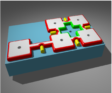
Our setup consists of four topological superconductors (TSs) each carrying a vortex and connected by constriction junctions; there is an additional vortex inside the loop of TSs (see Fig. 1). In order to reveal the topological property of the system, we first attach another TS to the device. We show that the edge MF of this TS can be driven in a controlled way around the loop of the four TSs by switching on and off gate voltages at constriction junctions in the designed sequence. After this process, the parity of this TS is flipped since the edge MF acquires a phase due to the vortex at the center of device. Therefore, one can consider this TS as a MF qubit, and the device of four TSs as a NOT gate. We then demonstrate that the NOT gate works for single electron pumping when a QD with Coulomb blockade effect is attached when the energy of QD is adjusted appropriately. Numerical simulations based on the time-dependent Bogloliubov-de-Gennes (TDBdG) equationOurPaper are performed, which confirms successfully the quantum protection and phase coherence during the whole process typically of several nano seconds.
The remaining part of this paper is organized as follows. We discuss in Sec. II the dynamics of an edge MF in a MF-qubit driven through the NOT gate. Then we reveal the relation satisfied by the interactions in the NOT gate in Sec. III. Based on the property of NOT gate, we formulate in Sec. IV the topological single electron pumping by attaching a QD to the NOT gate, and give explicitly the energy regime for QD. In Sec. V, it is clarified that the function of NOT gate can be understood as a quantum interference between two MFs. Discussions are presented in Sec. VI with a summary given in Sec. VII.
II Not gate for MF-qubit
A topological superconducting state can be achieved in a heterostructure of -wave superconductor (s-SC), spin-orbit coupling semiconductor (SOSM), and ferromagnetic insulator (FMI) with one vortex at the sample center, where one MF appears at the vortex core and another MF at the sample edge SauDasSarmaPRL10 ; OurPaper . In the present device, four finite TSs are positioned on a common -SC substrate. The core MFs are stable and do not participate in the phenomena discussed below (strictly speaking there are exponentially small contributions, which can be neglected safely), and thus will be omitted hereafter. The linear dimension of TSs should be in the regime of tens to one hundred nano metersOurPaper : for too large TSs, the energy gap between the zero-energy MF state and the lowest excited state becomes very small, which limits the operation temperature, while for too small TSs, core MF and edge MF interact with each other, which destroys the MF ground state. Edge MFs interact with neighboring ones through the constriction junctions when electron hoppings are permitted. There is an additional vortex in the s-SC substrate inside the loop formed by the four TSs, which governs the interactions among edge MFs as will be revealed below. We attach a MF qubit to the above device as schematically shown in Fig. 1.
The low-energy physics of the system can be described by the following effective Hamiltonian,
| (1) |
where denotes the edge MF at the qubit, and with denote those on the TSs in the NOT gate and ; time-dependent, dimensionless factors are introduced for the switching process of constriction junctions, whereas are the MF interactions when the gate voltage is off and thus two TSs are connected fully.
At the initial stage, the switch configuration is described by the vector (see the left inset of Fig. 2). Since the qubit is isolated, there is an edge MF () localized at the qubit. In contrary, with , both the unified edge of TS(1) and TS(2) and that of TS(3) and TS(4) contain two vortices, and thus there is no edge MF in the NOT gate. In the representation of 1, the MFs for are fused to finite energies due to the interactions.
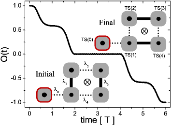
Turning on the connection between the qubit and TS(1), namely , the wavefunction of spreads to the unified edge of the now connected qubit, TS(1) and TS(2), since it contains three vortices. We then turn off the connection between TS1 and TS2, namely . The wavefunction of edge MF collapses totally on TS2 due to the topological property. After these two switchings, the edge MF is transported completely to TS2. Repeating this process, one can drive the edge MF through the NOT gate in a clockwise way, and returns it back to the initial position at the qubit, with the switching sequence . During this process the edge MF feels the gauge field formed by the central vortex, and thus acquires a phase of which makes . As the result, the electronic parity of the qubit is flipped.
In order to confirm the function of the NOT gate, we perform numerical calculations based on TDBdG equation. We first diagonalize the tight-binding BdG hamiltonian OurPaper of the system in the initial stage,
| (2) |
where both spin-conserved hopping and spin-flipped hopping are between nearest neighbors with the grid spacing, and is the Zeemann energy. An edge MF state is obtained at the MF qubit with the wave function . Then we modulate dynamically the hopping parameters at the constriction junctions, which changes the MF interactions in 1 sequentially and drives the edge MF OurPaper . The evolution of the wave function is obtained by solving the TDBdG equation based on the Chebyshev polynomials expansiontdbdg_1 ; tdbdg_2 . To monitor the evolution of the edge MF, we project the wave function onto the initial one, and evaluate the parameter . As can be seen from Fig. 2, changes from positive unity at the initial stage to negative unity at the final stage, representing a sign change in the MF wave function. It is worth noticing that the conservation of the function norm as seen in Fig. 2 confirms the topological protection of the edge MF during the operating process.
III Parity flipping in NOT gate
Since the parity of the whole system is conserved upon application of gate voltage as well as Cooper pair tunneling from SC substrate, the above switching operation should reverse the parities of the MF qubit and NOT gate simultaneously. In order to check the electronic parity of the NOT gate, we investigate first the signs of MF interactions defined in Eq. (1). As revealed in the previous workOurPaper , when is transported to TS(2), it picks a sign sgn(). Therefore, the sign of edge MF after driven through the NOT gate is given in terms of the interactions by
| (3) |
The minus sign attached to is due to the opposite motion of MF against the direction used to define the interaction in 1OurPaper .
It is then clear that the sign reversal of implies , a topological property generated by the central vortex. Hereafter, we consider explicitly the case where all interactions are positive since all possible configurations of interaction signs can be transformed to each other by gauge transformation. It is worth noting that the same sign constraint and gauge choice are available for even number of TSs, which will be used for discussions below.
We define two regular electronic states with the four MFs, and , as always possible even when the MFs are bounded and not free. We then rewrite the Hamiltonian 1 in terms of the basis , with denoting the parity of the electronic state,
| (4) |
where . The four eigen energies are given by for even parity, and for odd parity. The switch configuration of the constriction junctions in the NOT gate changes after the operation: and at the initial stage, while and at the final stage. It is clear that the ground-state energy at the initial stage is achieved in the even-parity subspace, while at the final stage in the odd-parity subspace. Therefore, the electronic parity of the NOT gate is reversed after the operation of switching. It is easy to see that this parity reversal is realized because .
IV Single electron pumping
The NOT gate discussed above can be used for single electron pumping when a QD is attached (see Fig. 3(a)). The parity flipping specifies an odd number of electrons transferring between the NOT gate and QD upon the switching operation described above, whereas the Coulomb blockade effect on the QD limits the charge transfer to a single electron.
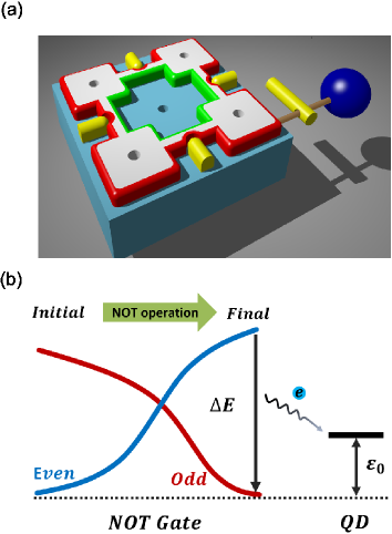
Let us first consider the case of a vacant QD with an energy level in the initial stage (see Fig. 4(b)). The ground state of the total system exhibits even parity, since the NOT gate is in a state of even parity. From the parity conservation of the total system, there are two candidates for the ground state at the final stage after switching operation discussed above: vacant QD with total energy , and/or occupied QD with total energy , both exhibit even parity. One electron on the NOT gate is transferred to the QD upon the switching operation if , namely . Physically the inequality means that if the occupation energy of the QD is too large, electron will not jump to QD. In the same way, one can figure out that when QD is occupied at the initial stage, an electron is transferred to the NOT gate upon switching operation if , namely . The physical meaning of the condition is also clear.
In order to perform single electron pumping starting from a switch configuration opposite to the one discussed above, one has two similar conditions on and . Therefore, the necessary and sufficient condition for single electron pumping is .
V Quantum interference of MFs
The parity flipping in the NOT gate discussed above can be understood generally as a quantum interference of MFs. We consider a loop of TSs with a vortex at the center of the common superconducting substrate. At the initial state, the odd/even constriction junctions are on/off, with no edge MF in the system. First, we turn off , which produces two edge MFs and on TS(1) and TS(2) respectively. By turning on and , and then turning off and , and so on so forth, the MF and are transported to TS(2l) and TS(2l+1) respectively. Finally, we turn on , which annihilates the two MFs.
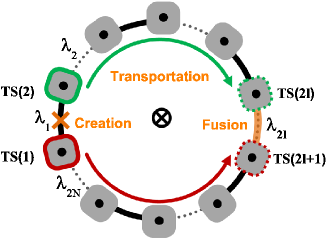
After the above sequence of switchings, the odd/even constriction junctions become off/on, opposite to the initial configuration. Let us check the ground-state electronic parity for the two configurations, keeping in mind that all the coupling constants are positive when switched on as the topological property revealed explicitly for the NOT gate with four TSs. The ground state at the initial configuration is a fully occupied state by electrons defined by for . The electronic parity of the whole system has the eigen value .
For the final configuration, the ground state is a fully occupied state by electrons defined alternatively by with . Its electronic parity can be calculated as
| (5) |
which is opposite to the one of the initial configuration. It is noticed that when the system of TSs is isolated, the parity should be preserved, and thus the true ground state with reserved parity cannot be achieved. The attachment of a MF qubit or a QD assists the parity flipping as discussed above.
It is easy to prove that without the central vortex, or generally with an even number of vortices, a system of TSs takes the same ground-state parity after switching. Therefore, with an odd number of central vortices, the quantum interference of two MFs is constructive, which flips the ground-state parity, whereas with an even number of central vortices, the quantum interference is destructive leaving no parity change in the system. Quantum inference of MFs was discussed for a system with superconductor and two ferromagnets on the surface of topological insulatorAkhmerov_Beenakker_prl09 . The two phenomena share the same topological origin induced by the central vortex. However, in the present case, the parity is reversed upon the switching process, whereas in the case addressed before an injected electron at one lead induces either emission or absorbtion of an electron (strictly speaking, odd number of electrons), which preserves the parity.
VI Discussions
The mechanism of single electron pumping in the present proposal is different from previous ones in literature BiasCQ ; PWBrouwer ; AdiaCQ . Unlike the case where electrons are driven by biased potentials between QD and electrodesBiasCQ , we switch the coupling between QD and the charge reservoir, i.e. the NOT gate, instead of the bias. Since the present single electron pumping is independent of the details of the switching process as far as it is slow enough, it is also different from the previous adiabatic pumping schemes where the details of pumping parameters during the operations have a significant effect on the direction and magnitude of the pumping currentPWBrouwer ; AdiaCQ . In this sense, the present scheme can be called topological charge pumping.
In our schemes, the manipulation of edge MFs is topologically protected by edge excitation gap which sets the limitation of the working temperature. For a sample size of 150150nm2, the edge excitation gap is estimated as 0.01 with the superconduction pair potential OurPaper . For =1meV, the gap is , which is not hard to achieve experimentally in these days. It is worthy to note that there is a work by Akhmerov showing that even the occupation of higher in-gap excitations will not violate the topological protection AkhmerovPRB10 .
VII Summary
In conclusion, we reveal that the mobility of Majorana fermion at edge of nano topological superconductor induced by a vortex can be used to implement a quantum NOT gate for Majorana qubit. The working mechanism for the NOT gate can be understood as the Aharonov-Bohm interference of two Majorana fermions. Based on this phenomenon, we formulate a scheme for topological single electron pumping. Useful applications of these devices in quantum transport and quantum computation are expected.
Acknowledgements This work was supported by WPI Initiative on Materials Nanoarchitectonics, MEXT of Japan, and Grants-in-Aid for Scientific Research (No.22540377), JSPS, and partially by CREST, JST. Q.F.L. is also supported by NSFC under grants 10904092.
References
- (1) K. von Klitzing, G. Dorda, and M. Pepper, Phys. Rev. Lett. 45, 494 (1980); K. von Klitzing, Rev. Mod. Phys. 58, 519 (1986).
- (2) B. D. Josephson, Phys. Lett. 1, 251 (1962); ibid Rev. Mod. Phys. 36, 216 (1964).
- (3) S. Giblin, M. Kataoka, J. Fletcher, P. See,T. J. B. M. Janssen, J. P. Griffiths, G. A. C. Jones, I. Farrer and D. A. Ritchie, Nat. Commun. 3, 930(2012); and references therein.
- (4) W. Lu, Z. Ji, L. Pfeiffer, K. W. West and A. J. Rimberg, Nature(London) 423, 422 (2003).
- (5) T. Fujisawa, T. Hayashi, Y. Hirayama, H. D. Cheong and Y. H. Jeong, Appl. Phys. Lett. 84, 2343 (2004).
- (6) M. H. Devoret, D. Esteve and C. Urbina, Nature(London) 360, 547 (1992).
- (7) P. W. Brouwer, Phys. Rev. B 58, 10135 (1998).
- (8) M. Switkes, C. M. Marcus, K. Campman and A. C. Gossard, Science 183, 1905 (1999).
- (9) S. H. Simon, Phys. Rev. B 61, 16327(2000).
- (10) G. Moore and N. Read, Nuc. Phys. B 360, 362 (1991).
- (11) N. Read and D. Green, Phys. Rev. B 61, 10267 (2000).
- (12) D. A. Ivanov, Phys. Rev. Lett. 86, 268 (2001).
- (13) A. Y. Kitaev, Phys. -Usp. 44, 131 (2001).
- (14) A. Y. Kitaev, Ann. Phys. 303, 2 (2003).
- (15) S. Das Sarma, M. Freedman and C. Nayak, Phys. Rev. Lett. 94, 166802 (2005).
- (16) S. Tewari, S. Das Sarma, C. Nayak, C. -W. Zhang and P. Zoller, Phys. Rev. Lett. 98, 010506 (2007).
- (17) M. Sato, Y. Takahashi and S. Fujimoto, Phys. Rev. Lett. 103, 020401 (2009).
- (18) S. Tewari, S. Das Sarma and D. -H. Lee, Phys. Rev. Lett. 99, 037001 (2007).
- (19) L. Fu and C. L. Kane, Phys. Rev. Lett. 100, 096407 (2008).
- (20) F. Wilczek, Nat. Phys. 5, 614 (2009).
- (21) A. R. Akhmerov, J. Nilsson and C. W. J. Beenakker, Phys. Rev. Lett. 102, 216404 (2009).
- (22) J. D. Sau, R. M. Lutchyn, S. Tewari and S. Das Sarma, Phys. Rev. Lett. 104, 040502 (2010).
- (23) R. M. Lutchyn, J. D. Sau and S. Das Sarma, Phy. Rev. Lett. 105, 077001 (2010)
- (24) Y. Oreg, G. Rafael and F. von Oppen, Phys. Rev. Lett. 105, 177002 (2010).
- (25) J. Alicea, Y. Oreg, G. Refael, F. von Oppen and M. P. A. Fisher, Nat. Phys. 7, 412 (2011).
- (26) C. Nayak, S. H. Simon, A. Stern, M. Freedman and S. Das Sarma, Rev. Mod. Phys. 80, 1083 (2008).
- (27) Q. -F. Liang, Z. Wang and X. Hu, Europhys. Lett. 99, 50004 (2012).
- (28) M. Bollhöfer and Y. Notay, Comp. Phys. Com. 177, 951 (2007).
- (29) S. Roche, Phys. Rev. B 59, 2284 (1999).
- (30) Y. L. Loh, S. N. Taraskin and S. R. Elliott, Phys. Rev. Lett. 84, 2290 (2000).
- (31) A. R. Akhmerov, Phys. Rev. B, 82, 020509(R) (2010).