Variability Improvement by Interface Passivation and EOT Scaling of InGaAs Nanowire MOSFETs
Abstract
High performance InGaAs gate-all-around (GAA) nanowire MOSFETs with channel length () down to 20nm have been fabricated by integrating a higher-k LaAlO3-based gate stack with an equivalent oxide thickness of 1.2nm. It is found that inserting an ultrathin (0.5nm) Al2O3 interfacial layer between higher-k and InGaAs can significantly improve the interface quality and reduce device variation. As a result, a record low subthreshold swing of 63mV/dec has been demonstrated at sub-80nm for the first time, making InGaAs GAA nanowire devices a strong candidate for future low-power transistors.
Index Terms:
Variability, MOSFET, InGaAs, nanowire.I Introduction
III-V compound semiconductors have recently been explored as alternative channel materials for future CMOS technologies [1]. InxGa1-xAs gate-all-around (GAA) nanowire MOSFETs fabricated using either bottom-up [2, 3] or top-down technology [4, 5, 6] are of particular interest due to their excellent electrostatic control. Although the improvement of on-state and off-state device metrics has been enabled by nanowire width () scaling, the scalability of the devices in [4] is greatly limited by the large equivalent oxide thickness () of 4.5nm. Aggressive scaling is required to meet the stringent requirements on electrostatic control [7, 8, 5]. It is shown recently that sub-1nm with good interface quality can be achieved by Al2O3 passivation on planar InGaAs devices [9]. Considering the inherent 3D nature of the nanowire structure, whether such a gate stack technology can be successfully integrated in the InGaAs nanowire MOSFET fabrication process remains to be shown. In addition, the electron transport in the devices [4] can be enhanced by increasing the Indium concentration in the InGaAs nanowire channel, which promises further on-state metrics improvements such as on-current () and transconductance ().
In this letter, we fabricated In0.65Ga0.35As GAA nanowire MOSFETs with atomic layer deposited (ALD) LaAlO3-based gate stack (=1.2nm). ALD LaAlO3 is a promising gate dielectric for future 3D transistors because of its high dielectric constant (k=16), precise thickness control, excellent uniformity and conformality [10]. The effect of ultra-thin Al2O3 insertion on the device on-state and off-state characteristics has been systematically studied. It is shown that Al2O3 insertion effectively passivates the LaAlO3/InGaAs interface, leading to the improvement in both device scalability and variability. Record low subthreshold swing (SS) of 63mV/dec has been achieved at sub-80nm , indicating excellent interface quality and gate electrostatic control. Detailed device variation analysis has been presented for the first time for InGaAs MOSFETs, which helps identify new manufacturing challenges for future logic devices with high mobility channels.
II Experiment
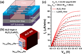
Fig. 1(a) and (b) show the schematic diagram and cross sectional view of InGaAs GAA nanowire MOSFETs fabricated in this work. The fabrication process is similar to that described in [4]. A HCl-based wet etch process was used to release the InGaAs nanowires with minimum of 20nm. Each device had 4 nanowires in parallel as shown in Fig. 1(a). Because of the relatively high etch selectivity between InAlAs and InP, an additional 100nm InAlAs etch stop layer was added under the 80nm InP sacrificial layer to improve the control of the nanowire release process. The InGaAs nanowire channel consists of one 10nm In0.53Ga0.47As layer sandwiched by two 10nm In0.65Ga0.35As layers shown in Fig. 1(b), yielding a total nanowire height () of 30nm. Here the heterostructure design ensures the high quality epitaxial layers grown by molecular beam epitaxy while maximizing the Indium concentration in the nanowire. A 0.5nm Al2O3, 4nm LaAlO3, and 40nm WN high-k/metal gate stack were grown by ALD surrounding all facets of the nanowires. Two samples were fabricated in parallel with only the sequence of the Al2O3 and LaAlO3 growth deliberately switched. Both samples were treated with 10% (NH4)2S, and then transferred into the ALD chamber within 1 minute of air break. Since the Al2O3-first and LaAlO3-first sample had the same of 1.2nm and underwent the same process flow, the difference of device performance can be ascribed to the effect of the Al2O3 passivation. All other fabrication details can be found in [4]. In this letter, the channel length () is defined as the width of the electron beam resist in the source/drain implantation process and has been verified by scanning electron microscopy.
III Results and discussion
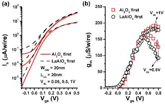
Fig. 1(c) shows the output characteristics of two representative Al2O3-first and LaAlO3-first InGaAs GAA nanowire MOSFETs with . Fig. 2(a) and (b) show the transfer characteristics and transconductance of the same devices. Due to the large junction leakage current in the drain, the source current is shown in the current-voltage characteristics and used to calculate and . The Al2O3-first device shows higher A/wire at and peak transconductance S/wire at , compared to 48A/wire and 155S/wire for the LaAlO3-first device. Both devices operate in enhancement-mode, with a linearly extrapolated of 0.14V and 0.11V, respectively. For the off-state performance, the Al2O3-first device shows a of 75mV/dec and of 40mV/V, while the LaAlO3-first device shows higher of 80mV/V and higher of 73mV/V.
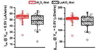
To study the statistical distribution of the on-state metrics, the box plots for and at are shown in Fig. 3. The box plots include measurements from all 50 devices with of 20nm and of 20nm. Although only a 12% (10%) increase in mean () is observed for the devices with Al2O3 insertion, a 54% (64%) reduction in standard deviation of () is obtained on the Al2O3-first devices, indicating a significant improvement in device variation by effective passivation of interface traps. The variation is impacted by several variation sources including parasitic resistance, effective mobility and variation [11], all of which are sensitive to the interface quality of the high-k/InGaAs nanowire surface.
To further investigate the scalability and off-state performance variability, the averages and standard deviations of , and as a function of are shown in Fig. 4 for Al2O3-first and LaAlO3-first devices with . The and remain almost constant with scaling down to 50nm for both samples. This indicates that the current GAA structure with 1.2nm has yielded a very small geometric screening length and the devices show excellent resistance to short channel effects. Average mV/dec and mV/V are obtained for Al2O3-first devices with between 50 and 80nm, compared to 79mV/dec and 39mV/V for the LaAlO3-first devices, indicating a reduction of interface trap density () with Al2O3 passivation. A small increase in is also observed for the Al2O3-first sample, which is ascribed to the reduction in negative donor-type charges at the interface.
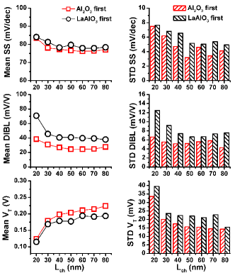
Furthermore, larger standard deviations of , and are observed for devices without Al2O3 insertion at all , indicating that the relatively low interface quality of the LaAlO3-first devices introduced additional device variation. It is also shown that the off-state performance variation increases as scales below 50nm, which is ascribed to the reduction in electrostatic control.
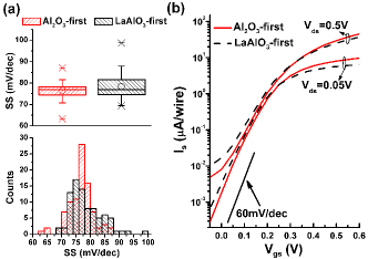
Fig. 5(a) show the box plot and histogram of measured from all the Al2O3-first and LaAlO3-first devices with between 5080nm and of 20nm. Although the average for Al2O3-first devices is only 1.9mV/dec lower than LaAlO3-first devices, 25% and 46% reduction in standard deviation and interquartile range has been obtained on Al2O3-first devices, indicating the effectiveness of Al2O3 passivation. Since these devices are immune to short channel effects, the is dominated by . Therefore, can be estimated from using the following equation,
| (1) |
where is the temperature in Kelvin, is the electronic charge, and is the oxide capacitance. 90% of the devices with Al2O3 insertion show between mV/dec, corresponding to a between cm-2eV-1. Fig. 5(b) shows the transfer characteristics of an 80nm hero Al2O3-first device and a 60nm hero LaAlO3-first device with the lowest mV/dec and 69mV/dec, respectively. The estimated for these two devices are and cm-2eV-1. The near-ideal is achieved because of the surface area of the nanowires, aggressive EOT scaling, and effective interface passivation.
IV Conclusion
InGaAs GAA nanowire MOSFETs with down to 20nm and down to 1.2nm have been demonstrated, showing excellent gate electrostatic control. The insertion of an ultra-thin 0.5nm Al2O3 between LaAlO3/InGaAs interface has shown to effectively improve the scalability and variability of the devices. Near-60mV/dec is achieved on InGaAs nanowires with scaled and effective interface passivation. The InGaAs GAA nanowire MOSFET is a promising candidate for low-power logic applications beyond 10nm.
Acknowledgment
The authors would like to thank A. T. Neal, M. S. Lundstrom, D. A. Antoniadis, and J. A. del alamo for the valuable discussions.
References
- [1] J. A. del Alamo, “Nanometre-scale electronics with III-V compound semiconductors,” Nature, vol. 479, no. 7373, pp. 317–323, Nov. 2011.
- [2] C. Thelander, C. Rehnstedt, L. Froberg, E. Lind, T. Martensson, P. Caroff, T. Lowgren, B. Ohlsson, L. Samuelson, and L.-E. Wernersson, “Development of a vertical wrap-gated InAs FET,” IEEE Transactions on Electron Devices, vol. 55, no. 11, pp. 3030–3036, 2008.
- [3] K. Tomioka, M. Yoshimura, and T. Fukui, “Vertical In0.7Ga0.3As nanowire surrounding-gate transistors with high-k gate dielectric on Si substrate,” in IEDM Tech. Dig., 2011, pp. 33.3.1–33.3.4.
- [4] J. J. Gu, Y. Q. Liu, Y. Q. Wu, R. Colby, R. G. Gordon, and P. D. Ye, “First experimental demonstration of gate-all-around III-V MOSFETs by top-down approach,” in IEDM Tech. Dig., 2011, pp. 769–772.
- [5] J. J. Gu, X. W. Wang, H. Wu, J. Shao, A. T. Neal, M. J. Manfra, R. G. Gordon, and P. D. Ye, “20-80nm channel length InGaAs gate-all-around nanowire MOSFETs with EOT=1.2nm and Lowest SS=63mV/dec,” in IEDM Tech. Dig., 2012, pp. 633–666.
- [6] F. Xue, A. Jiang, Y.-T. Chen, Y. Wang, F. Zhou, Y.-F. Chang, and J. Lee, “Excellent Device Performance of 3D In0.53Ga0.47As Gate-Wrap-Around Field-Effect-Transistors with High-k Gate Dielectrics,” in IEDM Tech. Dig., 2012, pp. 629–632.
- [7] M. Radosavljevic, G. Dewey, D. Basu, J. Boardman, B. Chu-Kung, J. Fastenau, S. Kabehie, J. Kavalieros, V. Le, W. Liu, D. Lubyshev, M. Metz, K. Millard, N. Mukherjee, L. Pan, R. Pillarisetty, W. Rachmady, U. Shah, H. Then, and R. Chau, “Electrostatics improvement in 3-D tri-gate over ultra-thin body planar InGaAs quantum well field effect transistors with high-K gate dielectric and scaled gate-to-drain/gate-to-source separation,” in IEDM Tech. Dig., 2011, pp. 33.1.1–33.1.4.
- [8] M. Egard, L. Ohlsson, B. Borg, F. Lenrick, R. Wallenberg, L.-E. Wernersson, and E. Lind, “High transconductance self-aligned gate-last surface channel In0.53Ga0.47As MOSFET,” in IEDM Tech. Dig., 2011, pp. 13.2.1–13.2.4.
- [9] R. Suzuki, N. Taoka, M. Yokoyama, S. Lee, S. H. Kim, T. Hoshii, T. Yasuda, W. Jevasuwan, T. Maeda, O. Ichikawa, N. Fukuhara, M. Hata, M. Takenaka, and S. Takagi, “1-nm-capacitance-equivalent-thickness HfO2/Al2O3/InGaAs metal-oxide-semiconductor structure with low interface trap density and low gate leakage current density,” Applied Physics Letters, vol. 100, no. 13, p. 132906, 2012.
- [10] J. Huang, N. Goel, H. Zhao, C. Kang, K. Min, G. Bersuker, S. Oktyabrsky, C. Gaspe, M. Santos, P. Majhi, P. Kirsch, H.-H. Tseng, J. Lee, and R. Jammy, “InGaAs MOSFET performance and reliability improvement by simultaneous reduction of oxide and interface charge in ALD (La)AlOx/ZrO2 gate stack,” in IEDM Tech. Dig., 2009, pp. 1–4.
- [11] T. Matsukawa, Y. Liu, S. O’uchi, K. Endo, J. Tsukada, H. Yamauchi, Y. Ishikawa, H. Ota, S. Migita, Y. Morita, W. Mizubayashi, K. Sakamoto, and M. Masahara, “Decomposition of on-current variability of nMOS FinFETs for prediction beyond 20 nm,” IEEE Transactions on Electron Devices, vol. 59, no. 8, pp. 2003–2010, August 2012.