Proposed Graphene Nanospaser
Spaser (Surface Plasmon Amplification by Stimulated Emission of Radiation) Bergman and Stockman (2003); Stockman (2008, 2010); Noginov et al. (2009); Hill et al. (2009); Oulton et al. (2009); Lu et al. (2012), which is a nanoplasmonic counterpart of laser, consists of a plasmonic nanoparticle coupled to an active (gain) medium. Spasing results in coherent generation of surface plasmons with nanolocalized, intense, coherent optical fields. One of the limitations on the spaser is posed by a high damping rate of the surface plasmon excitations in plasmonic metals. Here, we propose a novel nanospaser in the mid-infrared utilizing a nanopatch of graphene as its plasmonic core and a quantum-well cascade as its gain medium. This design takes advantage of low optical losses in graphene due to its high electron mobility Novoselov et al. (2005); Zhang et al. (2005). In contrast with earlier designs of quantum cascade lasers using plasmonic waveguides Sirtori et al. (1995); Tredicucci et al. (2000) and subwavelength resonators Walther et al. (2010), the proposed quantum cascade graphene spaser generates optical fields with unprecedented high nanolocalization, which is characteristic of graphene plasmons Thongrattanasiri and de Abajo (2013). This spaser will be an efficient nanosource of intense and coherent hot-spot fields in the mid-infrared spectral region with wide perspective applications in mid-infrared nanoscopy, nanospectroscopy, nanolithography, and optoelectronic information processing.
Quantum nanoplasmonics is becoming a fast-growing field of nanooptics Stockman (2011) due to unique property of plasmonic system to enhance strongly subwavelength optical fields while maintaining their quantum properties. The plasmonic enhancement is a basis of many applications of nanoplasmonicsMoskovits (1985); Xu et al. (1999); Tang et al. (2008); Nagatani et al. (2006). There is especial interest in mid-infrared near-field spectroscopy because of distinct spectral signatures of important molecular, biological, and condensed-matter systems, including macromolecules and graphene Huber et al. (2005); Fei et al. (2012). For further development of plasmonics and near-field optics and their applications, it is crucial to have a coherent source of intense local fields on the nanoscale, in particular, in the mid-infrared.
Here, we propose a novel spaser as coherent quantum generator of surface plasmons in nanostructured graphene. The plasmonic core of this spaser is a graphene-monolayer nanopatch, and its active (gain) element is a cascade quantum well system with a design similar to the design of an active element of quantum cascade lasers – see Fig. 1 (a).
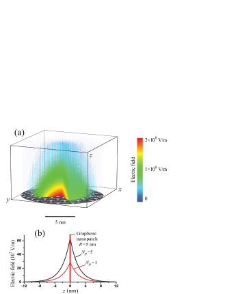
Graphene is a layer of crystalline carbon that is just one atom thick Geim and Novoselov (2007); Neto et al. (2009); Abergel et al. (2010). Its low-energy electronic excitations are described by the chiral relativistic massless Dirac-Weyl equation. Doped graphene is known to posses plasmonic properties with a potentially high plasmonic quality factor (low optical loss) due to high electron mobility Novoselov et al. (2005); Zhang et al. (2005); Koppens et al. (2011); Jablan et al. (2009); Grigorenko et al. (2012); Fei et al. (2012). The size of the graphene nanopatch may be as small as nm. Graphene possesses unprecedented tight localization of local plasmonic fields at the surface, which provides an unique opportunity to build an electrically-pumped mid- to near-infrared nanospaser with coherent optical fields of extremely high concentration and intensity – see Fig. 2. This will be the first electrically pumped nanospaser: the previous nanospasers were optically pumped Noginov et al. (2009); Lu et al. (2012) while the electrically pumped spasers had mode volumes of microscale size at least in one dimension Hill et al. (2009); Oulton et al. (2009).
The chiral nature of the electronic states in graphene results in strong suppression of electron scattering, which greatly increases the mobility of charge carriers Novoselov et al. (2005) and greatly reduces the theoretically-estimated plasmonic losses Koppens et al. (2011). For plasmon frequency below the interband loss threshold, , where is the Fermi energy of graphene, and below the optical phonon frequency, , the plasmon relaxation time can be estimated from direct-current measurements. In unsuspended graphene, the high static carrier mobility of Zhang et al. (2005); Jablan et al. (2009) is realized at carrier density , which corresponds to eV, where is Fermi velocity Kim et al. (2012). For such mobility, the plasmon relaxation time in graphene can be estimated as ps. This yields plasmon quality factor at frequency meV.
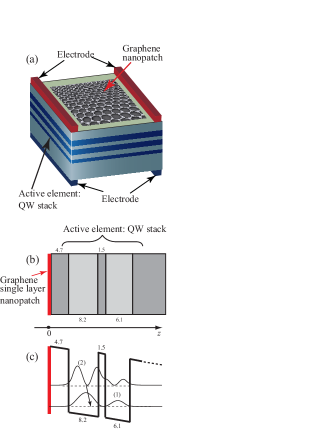
As the active element of the graphene spaser, we consider a multi-quantum well system, which is similar to the design of the active element of quantum cascade laser Kazarinov and Suris (1971); Faist et al. (1994). Within the active region of such a multi-quantum well structure, optical transitions occur between subband levels of dimensional quantization in the growth direction.
In the graphene spaser, we utilize only one period (a single multi-quantum well heterostructure) from the active medium of the quantum cascade laser – see Fig. 1 where one of possible designs of the active medium is illustrated. The functioning of such an active medium is characterized by fast and efficient electrical injection of electrons into the upper subband level of the multi-quantum well system and their extraction from the lower subband level – see Fig. 1 (c). Since the plasmonic modes of graphene are strongly localized in the normal direction (i.e., in the growth direction of the quantum wells, along the axis in Fig. 1), with localization length nm, only one period of the quantum cascade gain medium couples to the plasmonic modes of graphene. The gain, i.e., population inversion, in the quantum well system is introduced through a voltage applied to the system.
To find plasmonic modes of graphene, we assume that the graphene monolayer is surrounded by two homogeneous media with dielectric constants and . Effectively, this approximation amounts to replacement of the cascade system with a homogeneous effective medium.We assume that graphene monolayer is positioned in a plane . Its plasmon wave function (electric field) in the upper half plane () is and in the lower half plane () is , where is the in-plane wave vector and and are the decay constants in the upper and lower half planes, respectively.
In the Drude approximation, we obtain [see Eq. (8) of Supplementary Information (SI)] the well-known dispersion relation in graphene for a TM plasmon mode with frequency and wave vector ,
| (1) |
where electron polarization relaxation rate determines plasmon dephasing time .
In the quantum description of the graphene spaser, we introduce the Hamiltonian of the spaser in the form
| (2) | |||||
where the first sum describes the Hamiltonian of the gain medium, which consists of two subbands and (see Fig. 1) with energies and , respectively, . Here is electron effective mass, and is a two-dimensional electron wave vector. The second sum in Eq. (2) is the Hamiltonian of plasmons in the graphene layer, where and are operators of annihilation and creation of a plasmon with wave vector [see Eq. (9) of SI]. The last sum is the interaction Hamiltonian, , of plasmonic field with dipole of the gain medium.
Quantization of graphene surface plasmons yields modes [see Eqs. (1)-(2) and (11) of SI] that possess extremely tight nano-confinement at the graphene nanopatch surface as illustrated in Fig. 2. These local fields form a hot spot shown by the red color in Fig. 2 (a), which has the size of only a few nanometers in each of the three dimensions. These fields are coherent and their amplitude in this hot spot is very high, for one plasmon per mode; the field amplitude increases with the number of plasmons as . The unprecedented field localization characteristic of graphene and their high amplitudes inherent in nanospasers bear potential for various important applications, from nanospectroscopy and sensing to nanolithography.
The dipole interaction strength is determined by the corresponding Rabi frequency, ,
| (3) |
where we have taken into account that for intersubband transitions the dipole matrix element has only the component, and are electron wave functions with wave vector of subbands 1 and 2, respectively.
Assuming for simplicity that electron dynamics in the , , and directions is separable, we can factorize the wave functions, , where is a two-dimensional radius. Then Eq. (3) becomes
| (4) |
where is the intersubband envelope dipole matrix element, and is the distance between the graphene monolayer and the active quantum well of the cascade structure.
Introducing the density matrix of the active quantum well of the gain medium, , we describe the dynamics of the spaser within the density matrix approach, writing the equation for the density matrix, . For the stationary regime, we obtain the condition of spasing in the form Bergman and Stockman (2003); Stockman (2010)
| (5) |
where is the intersubband polarization-relaxation rate, and is the intersubband transition frequency. From this and Eq. (4), substituting from Eq. (12) of SI, we obtain
| (6) |
Here wave vector is an effective Fermi wave vector, i.e., the largest wave vector of the states, which are partially occupied by electrons in the gain region. Only such states contribute to the sum in Eq. (5).
At the resonance, i.e. at , the condition of spasing simplifies to
| (7) |
For given active region parameters, Eq. (7) introduces a constraint on plasmon polarization-relaxation rate .
Consider realistic parameters of the active region [corresponding, e.g., to the structure shown in Fig. 1 (b)]: meV, , and nm. A typical intersubband relaxation time in the quantum well cascade systems is ps Ferreira and Bastard (1989); Yamanishi et al. (2008). Under the resonant condition, the intersubband transition frequency meV, which is equal to the plasmon frequency, corresponds to the plasmon wave vector nm-1 – see Eq. (1). Realistically assuming that nm-1 and , we obtain
| (8) |
with the corresponding relaxation time s.
Substituting relation (1) into inequality (7), we obtain a spasing condition as a limitation on the plasmon polarization-relaxation time as
| (9) |
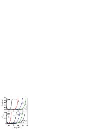
The dependence of the minimum plasmon relaxation time, , on the plasmon frequency is shown in Fig. 3(a) for different Fermi energies of electrons in graphene. The data clearly show that there is a broad range of plasmon frequencies in the mid-infrared eV where the required minimum relaxation time is relatively short, ps, so the spasing threshold condition (9) can realistically be satisfied. Outside this range, the minimum relaxation time greatly increases. Fortuitously, typical values of frequencies of intersubband transitions in quantum wells are within the same mid-infrared range eV.
The spasing condition of Eq. (9) can be also expressed in terms of dimensionless parameter – plasmon quality factor ,
| (10) |
Condition (10) on the surface plasmon quality factor depends in the plasmon frequency, , which under resonant condition is equal to the frequency of intersubband optical transitions in the active region of the cascade system. As a function of frequency , the minimum sufficient quality factor, , has a deep minimum, the position of which is determined by condition or . It depends on parameters of the system, such as the Fermi energy of electrons in graphene, , and the distance, , between the graphene monolayer and the active quantum well of the cascade structure. The dependence of on the frequency of surface plasmons, , is shown in Fig. 3(b) for different values of Fermi energy . The minimum value of is , and it does not depend on the Fermi energy, which affects only the position of this minimum. This minimum required quality factor of the plasmons is very low, indeed, which implies that the spasing is relatively easy to achieve. In fact, the quality factor value, , which is obtained for graphene from experimental data as discussed at the beginning in the introductory part of this Letter, is high enough, (it is on the same order as for silver in the visible regionStockman (2011)), for spasing to occur in a broad range of frequencies – see Fig. 3 (b).
Plasmon damping rate in graphene was measured experimentally by mid-infrared nanoscopy Fei et al. (2012). The best fit to the experimental data was obtained for rather strong damping or a low quality factor, , at plasmon frequency eV, which corresponds to plasmon relaxation time ps. Even for such strong plasmon damping, the plasmon quality factor, , is much greater than the minimum required value rate – see Fig. 3(b). Taking into account that the plasmon relaxation rate strongly increases above the optical phonon frequency, eV, we can conclude that the optimal Fermi energy in graphene should be eV. For such Fermi energy, the minimum of is realized at the plasmon frequency in the mid-infrared, eV – see Fig. 3(b). The above results clearly suggests that the spasing can be realized in realistic graphene systems coupled to quantum cascade well structures.
In conclusion, we predict that a graphene monolayer nanopatch deposited on a top of a specially designed stack of quantum wells constitutes an electrically-pumped spaser, which is a coherent source of surface plasmons and intense local optical fields in graphene in the mid-infrared. The system of quantum wells is designed similar to an active element of quantum cascade laser and is characterized by efficient electrical injection of electrons into an upper subband level of multi-quantum well system and fast extraction of electrons from a lower subband level. Under realistic parameters of the multiple quantum wells, our analysis shows that the condition of spasing, i.e., coherent generation of plasmons in graphene, can be achieved under realistic conditions at finite doping of graphene monolayer corresponding to electron Fermi energy in graphene eV. The above analysis can be applied not only to a graphene monolayer, but also for graphene-based nanoscale structures such as graphene nanoribbons, graphene quantum dots, and graphene nanoantennas, in particular, nanodimers where a possibility of efficient nanofocusing has been recently proposed Thongrattanasiri and de Abajo (2013). The predicted graphene spaser will be an efficient source of intense and coherent nanolocalized fields in the mid-infrared spectrum – cf. Fig. 2. With size of such a near-field localized mid-infrared source nm being on the same order of magnitude as important biological objects (viruses, cell organelles, chromosomes, large proteins or DNA) and technological elements (transistors and interconnects), such a spaser will have wide perspective applications in mid-infrared nanoscopy, nanospectroscopy, nanolithography, biomedicine, nano-optoelectronics, etc.
References
- Bergman and Stockman (2003) D. J. Bergman and M. I. Stockman, Phys. Rev. Lett. 90, 027402 (2003).
- Stockman (2008) M. I. Stockman, Nat. Phot. 2, 327 (2008).
- Stockman (2010) M. I. Stockman, Journal of Optics 12, 024004 (2010).
- Noginov et al. (2009) M. A. Noginov, G. Zhu, A. M. Belgrave, R. Bakker, V. M. Shalaev, E. E. Narimanov, S. Stout, E. Herz, T. Suteewong, and U. Wiesner, Nature 460, 1110 (2009).
- Hill et al. (2009) M. T. Hill, M. Marell, E. S. P. Leong, B. Smalbrugge, Y. Zhu, M. Sun, P. J. van Veldhoven, E. J. Geluk, F. Karouta, Y.-S. Oei, et al., Opt. Express 17, 11107 (2009).
- Oulton et al. (2009) R. F. Oulton, V. J. Sorger, T. Zentgraf, R.-M. Ma, C. Gladden, L. Dai, G. Bartal, and X. Zhang, Nature 461, 629 (2009).
- Lu et al. (2012) Y.-J. Lu, J. Kim, H.-Y. Chen, C. Wu, N. Dabidian, C. E. Sanders, C.-Y. Wang, M.-Y. Lu, B.-H. Li, X. Qiu, et al., Science 337, 450 (2012).
- Novoselov et al. (2005) K. S. Novoselov, A. K. Geim, S. V. Morozov, D. Jiang, M. I. Katsnelson, I. V. Grigorieva, S. V. Dubonos, and A. A. Firsov, Nature 438, 197 (2005).
- Zhang et al. (2005) Y. B. Zhang, Y. W. Tan, H. L. Stormer, and P. Kim, Nature 438, 201 (2005).
- Sirtori et al. (1995) C. Sirtori, J. Faist, F. Capasso, D. L. Sivco, A. L. Hutchinson, and A. Y. Cho, Appl. Phys. Lett. 66, 3242 (1995).
- Tredicucci et al. (2000) A. Tredicucci, C. Gmachl, F. Capasso, A. L. Hutchinson, D. L. Sivco, and A. Y. Cho, Appl. Phys. Lett. 76, 2164 (2000).
- Walther et al. (2010) C. Walther, G. Scalari, M. I. Amanti, M. Beck, and J. Faist, Science 327, 1495 (2010).
- Thongrattanasiri and de Abajo (2013) S. Thongrattanasiri and F. J. G. de Abajo, Phys. Rev. Lett. 110, 187401 (2013).
- Stockman (2011) M. I. Stockman, Opt. Express 19, 22029 (2011).
- Moskovits (1985) M. Moskovits, Rev. Mod. Phys. 57, 783 (1985).
- Xu et al. (1999) H. X. Xu, E. J. Bjerneld, M. Kall, and L. Borjesson, Phys. Rev. Lett. 83, 4357 (1999).
- Tang et al. (2008) L. Tang, S. E. Kocabas, S. Latif, A. K. Okyay, D. S. Ly-Gagnon, K. C. Saraswat, and D. A. B. Miller, Nat. Phot. 2, 226 (2008).
- Nagatani et al. (2006) N. Nagatani, R. Tanaka, T. Yuhi, T. Endo, K. Kerman, and Y. T. and. E Tamiya, Sci. Technol. Adv. Mater. 7, 270 (2006).
- Huber et al. (2005) A. Huber, N. Ocelic, D. Kazantsev, and R. Hillenbrand, Appl. Phys. Lett. 87, 081103 (2005).
- Fei et al. (2012) Z. Fei, A. S. Rodin, G. O. Andreev, W. Bao, A. S. McLeod, M. Wagner, L. M. Zhang, Z. Zhao, M. Thiemens, G. Dominguez, et al., Nature 487, 82 (2012).
- Geim and Novoselov (2007) A. K. Geim and K. S. Novoselov, Nat. Mater. 6, 183 (2007).
- Neto et al. (2009) A. H. C. Neto, F. Guinea, N. M. R. Peres, K. S. Novoselov, and A. K. Geim, Rev. Mod. Phys. 81, 109 (2009).
- Abergel et al. (2010) D. S. L. Abergel, V. Apalkov, J. Berashevich, K. Ziegler, and T. Chakraborty, Adv. Phys. 59, 261 (2010).
- Koppens et al. (2011) F. H. L. Koppens, D. E. Chang, and F. J. G. de Abajo, Nano Lett. 11, 3370 (2011).
- Jablan et al. (2009) M. Jablan, H. Buljan, and M. Soljacic, Phys. Rev. B 80, 245435 (2009).
- Grigorenko et al. (2012) A. N. Grigorenko, M. Polini, and K. S. Novoselov, Nat. Phot. 6, 749 (2012).
- Kim et al. (2012) S. Kim, I. Jo, D. C. Dillen, D. A. Ferrer, B. Fallahazad, Z. Yao, S. K. Banerjee, and E. Tutuc, Phys. Rev. Lett. 108 (2012).
- Kazarinov and Suris (1971) R. F. Kazarinov and R. A. Suris, Sov. Phys. Semicond. 5, 707 (1971).
- Faist et al. (1994) J. Faist, F. Capasso, D. L. Sivco, C. Sirtori, A. L. Hutchinson, and A. Y. Cho, Science 264, 553 (1994).
- Ferreira and Bastard (1989) R. Ferreira and G. Bastard, Phys. Rev. B 40, 1074 (1989).
- Yamanishi et al. (2008) M. Yamanishi, T. Edamura, K. Fujita, N. Akikusa, and H. Kan, IEEE J. Quantum Elect. 44, 12 (2008).
Acknowledgments
This work has been supported by Grant No. DE-FG02-11ER46789 from the Materials Sciences and Engineering Division and by Grant No. DE-FG02-01ER15213 from the Chemical Sciences, Biosciences and Geosciences Division, Office of the Basic Energy Sciences, Office of Science, U.S. Department of Energy. MIS acknowledges support by the Max Planck Society and the Deutsche Forschungsgemeinschaft Cluster of Excellence: Munich Center for Advanced Photonics (http://www.munich-photonics.de).
Competing financial interests
The authors declare no competing financial interests.