Present address: ]Department of Chemistry, University of Cambridge, Cambridge CB2 1EW, UK
A circuit analysis of an in situ tunable radio-frequency quantum point contact
Abstract
A detailed analysis of the tunability of a radio-frequency quantum point contact setup using a circuit is presented. We calculate how the series capacitance influences resonance frequency and charge-detector resistance for which matching is achieved as well as the voltage and power delivered to the load. Furthermore, we compute the noise contributions in the system and compare our findings with measurements taken with an etched quantum point contact. While our considerations mostly focus on our specific choice of matching circuit, the discussion of the influence of source-to-load power transfer on the signal-to-noise ratio is valid generally.
pacs:
07.50.Qx, 85.35.Be, 07.50.Ek, 84.30.-rI Introduction
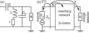
Understanding the electrical behavior of a given resonant circuit is key for maximizing the charge sensitivity of radio-frequency (rf) reflectometry experiments such as rf single-electron transistorlu:03 or quantum point contactmueller:07 ; reilly:07 ; cassidy:07 charge sensing. In view of this goal, Roschier et al.roschier:04 have presented a thorough analysis of the most commonly used matching network schoelkopf:98 . In this work, we pursue a rather similar purpose but focus on the circuitsillanpaa:04 ; sillanpaa:05 shown in Fig. 1(a) which can be adapted for in situ tunabilitymueller:10 . As we highly appreciate the detailedness of Ref. roschier:04, we shall try to keep up a similar level of depth while following a complementary path and highlighting different aspects.
We will start with a general observation on the influence of the fraction of available power actually delivered to the matched load on the system’s charge sensitivity in Sec. II. Subsequently, we will detail our choice of tunable matching circuit in Sec. III, whereafter our discussion will become specific to this type of circuit. Moreover we will calculate the maximally applicable voltage given a certain allowed voltage drop over the load and the corresponding input power. We will use these results to determine the network’s anticipated reaction to a change in the system’s charge state. In Sec. IV we will compute the relevant noise contributions and compare their magnitude to the charge-response in order to predict the detector’s charge sensitivity. Finally, we will verify our findings with measurements taken using a quantum point contact etched into the two-dimensional electron gas of a GaAs/AlGaAs heterostructure in Sec. V.
Since our research is directed towards quantum point contact (QPC) charge-detection on semiconductor quantum dots we assume the load to have a linear curve which facilitates the analysis compared to the use of a differential resistancekorotkov:99 . In real experimental life, however, this assumption may sometimes be inaccurate even at low bias as the exact potential landscape can drastically affect the characteristics.
II Power Transfer
In this first section we will deduce a general analytic expression for the signal-to-noise ratio (SNR) - inversely proportional to the square of the charge sensitivity - obtained with rf reflectometry measurements. To this end we have to compute the magnitude of the signal - given by the change in reflection coefficient upon addition of a single charge to the system times the input voltage - and the total noise voltage or power.
If any amount of power is applied to a matching network, only a certain fraction of the power supplied by the source is delivered to the load while another fraction is dissipated by the lossy circuit and a part is reflected. This situation is sketched in Fig. 1(b) which has been adapted from Ref. roschier:04, . There is a source with impedance connected to a transmission line with impedance leading to the matching network with -matrix directly connected to a load . While the load may have a complex impedance which can be utilized for instance in dispersive readoutpetersson:10 , we restrict ourselves to real values of . Nevertheless, generalization is readily obtained. Note that in reflectometry experiments the reflected wave is measured through an amplifier which, for simplicity, we assume to be matched to . Naturally, the fractions introduced above follow the equation
| (1) |
As shown for instance in the chapter on microwave amplifier design in Ref. pozar:11, and discussed in Ref. roschier:04,
| (2) | |||||
| (3) |
where are the matching network’s -matrix elements and
| (4) | |||||
| (5) |
The characteristic impedance of the rf lines is usually . For a matched source (which we will assume for the remainder of this work), is equal to zero, and Eq. (3) simplifies to
| (6) |
To go beyond this we will determine a generally valid expression for the reflection coefficient’s sensitivity on . Therefore, we calculate the absolute value of the differential change in via
| (7) |
as measured using in-phase and quadrature amplitudes in homodyne detection. Similarly, one could study the phase change or the change in absolute value of the reflection coefficient, for instance when relying on heterodyne detection.
The first part of Eq. (7) can be evaluated as
| (8) | |||||
using in reciprocal two-port networks. The second part of Eq. (7) is
| (9) |
Combining Eqs. (7), (8), and (9) thus yields
| (10) |
We want to stress that this analysis is valid for any reciprocal linear two-port network, independent of the specifics of , as long as can be linearized in over the range . It is important to bear in mind, though, that strongly depends on the load (charge detector) resistance and consequently, the largest change in reflection coefficient is not necessarily observed at maximum .
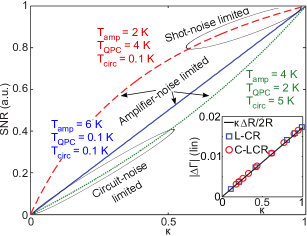
The change of the reflection coefficient as a function of , given by Eq. (10), is shown as the black line in the inset of Fig. 2 for a change in resistance from 29 to , realistic as a change in QPC resistance upon tunneling of an electron into or out of a proximal quantum dot. The blue squares (red circles) are calculations of where is determined from the impedance of a () circuit and is varied by introducing a parasitic resistance in series to (). The parameters - and in case of the circuit also - are chosen individually for every data point such that the load is matched at . Since Eq. (10) is exact as long as can be linearized over the range , the perfect agreement between the direct (blue squares and red circles) and indirect (black line) calculation is not particularly surprising.
Now that we know the circuit’s response, e.g. due to charge tunneling into a capacitively coupled quantum dot, we can compute the signal voltage by multiplying with the input voltage. If we need to limit the voltage drop over the load, henceforth assumed to be a QPC, to a given value - which is for instance necessary to avoid excessive back-action in charge-detection measurements - the tolerated input voltage and power are fixed throughroschier:04
| (11) | |||||
| (12) |
where is the amplitude of the voltage incident from the source to the -matrix and is the voltage applied to the load, which is the sum of incoming and reflected voltages, and is the power delivered to the entire network given by the difference between applied power and reflected power . Hence the signal amplitude, defined as the change of the amplitude of the wave reflected at the -matrix, is given by
| (13) |
For QPC charge detection, has been found to be a good compromise between the desire to maximize the signal but minimize back-actiongustavsson:07 .
By assigning an equivalent noise temperature to all relevant noise sources - QPC (, thermal and shot noise; typically a few K), matching network (, thermal noise; mK to a few K), and low-noise amplifier (; of the order of a few K for state-of-the-art devices) - we can conveniently express the overall noise as measured over the matched amplifier input resistor by
| (14) |
Note that the circuit noise temperature can be determined as the concerted action of two correlated noise sources at either input of the two-port network characterizing the matching cirucittwiss:55 . Also, we have chosen a simplified version of the amplifier noise temperature as compared to Ref. roschier:04, where a noise-wave description was used.
Thus, we can calculate the signal-to-noise ratio at the amplifier output via
| SNR | (15) | ||||
If is considered to be kept fixed we immediately arrive at
| (16) |
It should be emphasized that the SNR always increases with . Clearly, if there is no power transfer between source and load (), the signal-to-noise ratio vanishes, and if all the power is delivered to the load () the SNR is inversely proportional to .
The main graph of Fig. 2 visualizes Eq. (16) where the SNR is computed as a function of and normalized by for three different cases with (dashed red line), (solid blue line), and (dotted green line), respectivelyNoteTemp . In the first case for large power transfer the noise at the amplifier output is dominated by the load’s noise temperature - realistically QPC shot noise - while at low power transfer and in the second case the dominant contribution originates from the amplifier - which is the case for low QPC bias or comparably large amplifier noise. Note that the SNR for the case with is an almost straight line with a slope of roughly and always lies below the shot-noise limited case if the sum is equal for both cases. This follows from the suppression of with . If the matching network adds a considerable amount of thermal noise the SNR is poorer, which can be particularly painful at low power transfer.
If an experiment is dominated by amplifier noise, we can assume that the total noise temperature is independent of the QPC resistance. Then, since can be shown to be inversely proportional to for (see Eq. (6)), we obtain
| (17) |
where the last approximation is valid if .
We can also estimate the increase in SNR expected for experiments carried out in a dilution refrigerator as compared to a variable-temperature insert at 2 K; for a fixed amplifier noise temperature of 2 K and reducing as well as from 2 to and assuming , the signal-to-noise ratio is doubled. And this does not yet take into account that a nanostructure’s resistance typically becomes more sensitive to electrostatic potentials at lower temperatures.
From the above considerations it is clear that having low losses in the matching circuit - no matter which type - is crucial. Potential strategies to reduce losses are the use of low-loss printed circuit boards as well as superconducting air or on-chip inductorsxue:07 and waveguides.
With this we conclude the generally valid part and turn towards our choice of a tunable circuit.
III Tuning of the Matching Network
To compensate for large stray capacitances in parallel to the load when using a ceramics chip-carrier design or working with structures having large back gates such as graphene devicesmueller:12 , we have selected a circuit as a matching network. The series capacitance can then be set by an in situ tunable varactor diodemueller:10 . In the following we will investigate the effect of changing this capacitance on the frequency response, on matching at the resonance frequency, and on the maximal voltage and power we are allowed to send into the matching circuit.
| Variable | Description | Value |
|---|---|---|
| Tunable series capacitance | 1.5 pF | |
| Parallel (stray) capacitance | 2.6 pF | |
| Parallel inductance | 150 nH | |
| Parasitic resistance | 2 or 5 | |
| Load resistance | 50 k | |
| Amplifier noise temperature | 2 K | |
| Load noise temperature | 2 K | |
| Circuit noise temperature | 5 K |
Since we will be using numerous parameters, we define our standard set of numerical values in Tab. 1 for the reader’s comfort. Nevertheless, we will still continue to note the utilized values in the main text.
To facilitate our analysis we consider the simplified circuit model shown in Fig. 1(a). This circuit assumes all stray capacitances - which we will combine in the parameter - to be in parallel to the load and all losses of the matching network to be in series to the inductorNote1 (denoted by a resistance ), neglects inductances of all elements including bond wiresNote2 , and regards the load (QPC) as a purely real impedance . Comparing the calculated frequency response of this simplified circuit with a full circuit model including all the aspects mentioned above reveals that they are negligible indeed (not shown). The value of , however, must be determined from experimentally obtained matching curves and amounts to roughly when using a GaAs QPC etched into a shallow two-dimensional electron gas (with InAs nanowires deposited on top of the chip) as a load and an inductance of , for an etched graphene nanoconstriction and , or when matching an AFM-defined GaAs QPC (without nanowires) and with an inductance of Note3 . At this point we unfortunately cannot say where this rather large difference is originating from - a quite detailed investigation of the influence of the sample geometry (such as performed in Ref. hellmueller:12, ) and substrate used would be required for this.
The impedance of this simplified circuit is given by
| (18) |
If , , , and are assumed to be fixed by the circuit and the load, the matching conditions
| (19) | |||||
| (20) |
determine and . In particular, a tunable capacitance thus allows us to achieve perfect matching () for any provided that the range of is large enough.
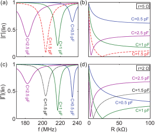
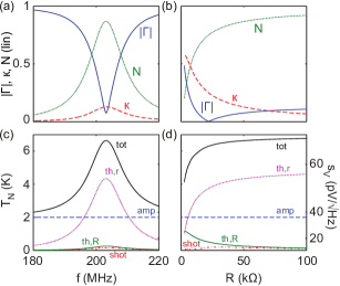
Calculating the frequency response of the reflection coefficient using Eqs. (2) and (18) for different series capacitances yields Figs. 3(a) and (c). For these calculations we have used , , , and (). We can clearly see that an increase in reduces the resonant frequency, as expected. Furthermore, both and alter the depth of the resonance. This is more easily visible in Figs. 3(b) and (d), where the reflection coefficient is calculated as a function of at the resonance frequency. The latter is determined by numerically finding the minimum of at . Increasing shifts the resistance for which optimal matching is achieved to lower values, while increasing shifts these values to higher . If is too large or if is too small perfect matching is never achieved. If is too large, optimal matching occurs at low resistances, where charge detectors are generally less sensitive. It can also be noted that the width of the resonance is decreasing with increasing resonance frequency.
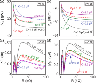
Now that we are convinced that we can obtain good matching through tuning of and selection of the proper measurement frequency we want to compute the magnitude of the signal we can expect for a given change in load resistance (due to the addition of charge on the quantum dot). Therefore we will first determine numerically the voltage and power we may apply if the voltage drop over the load should be maximally (see Eq. (11) in Sec. II). The value of can be calculated with Eq. (6) using -matricespozar:11 ; roschier:04 or, alternatively, using -matrices. Either way leads to the same result, and the maximal input voltage and the power thus delivered to the matching network (including load) at resonance are presented in Figs. 4 (a) and (b) for our usual parameters of , , and ( for the dotted black curve). It is visible that worse matching (see Fig. 3) means we can apply a higher voltage which is reasonable since in this case less signal couples to the load. For a parasitic resistance of the input voltage is in the range of , whereas for we are only allowed to apply . The powers delivered to the circuit are of the order of which is .
To assess the expected signal height we still need the change in reflection coefficient upon addition of a single charge to the system. Towards this end we focus again on QPC charge detection and model the QPC with a saddle-point potentialbuettiker:90 with and at . Then, we assume that the addition of a single unit charge to the charge detector’s environment changes its chemical potential by Note4 , since such a potential difference leads to a conductance change of up to which is quite realistic for an InAs nanowire quantum dot self-aligned to a GaAs QPCshorubalko:08 . In combination with the reflection coefficients obtained in Figs. 3(b) and (d) this estimated change in QPC conductance leads to a change in as shown in Fig. 4(c). The line shape of these curves originates from the step-like resistance behavior of a QPC. The magnitudes of the reflection coefficient changes amount from 0.01 for worse matching up to 0.03 (on a linear scale) for better matching. Since at superior matching the maximally allowed input voltage is smaller, the total reflected voltage determined by Eq. 13 and depicted in Fig. 4(d) depends less strongly on the quality of the matching, but still better matching and lower losses lead to a significantly higher signal amplitude. Signal amplitudes of several hundreds of nanovolts are thus quite realistic for a highly coupled dot-charge detector system.
We have now found a reliable estimate for the expected signal height by assessing the change in reflection coefficient due to a modeled change in QPC resistance and taking into account a maximally allowed voltage drop over the charge detector. In the next section we will compare this signal amplitude to the total noise in our system to predict the signal-to-noise ratio or charge sensitivity of our charge-detection measurements.
IV Noise Analysis
We will start this section by identifying and sizing the relevant noise sources in our measurement setup. The sum of these noise contributions will then be checked against the signal height assessed in the previous section to estimate the signal-to-noise ratio of a charge detection experiment.
The noise power spectral density of the QPC at frequencies much lower than temperature and voltage bias () is given bykhlus:87
| (21) | |||||
where denotes the energy-independent transmission of the -th channel occupied at through the QPC. As mentioned in Sec. II we can assign an effective noise temperature to this power spectral density via
| (22) |
In our experiments at an ambient temperature of , this is almost entirely dominated by thermal noise, but at dilution refrigerator temperatures, shot noise can easily exceed thermal noise, especially if a large source-drain bias can be applied. Since the network is reciprocal, the QPC’s noise temperature will contribute to the total setup noise proportionally to .
In contrast, low-frequency thermal noise in the parasitic resistor
| (23) |
transforms via the coefficient introduced previously. In our experiments we estimate the circuit noise temperature to be as high as , probably due to insufficient thermal anchoring of the printed circuit board and/or heating of the matching network by the low-temperature amplifier (due to spatial constraints there is no isolator between resonant circuit and amplifier in our experiments).
The frequency dependencies of the coefficients and as well as are shown in Fig. 5(a), using our usual circuit parameters. While matching is poor, most power is reflected and consequently and are small. Once power starts to be transmitted, the matching network and the load share the amount. The exact ratio between power delivered to the load an dissipated over the lossy matching network strongly depends on the specifics of the circuit, including the load resistance . This behavior is shown in Fig. 5(b). We want to draw attention to the tendency that the higher the load resistance, the more difficult it becomes to deliver power to it, which can also be seen from Eq. (6).
Finally the noise power of the low-noise amplifier is denoted by its noise temperature . For a state-of-the-art low-noise amplifier this can be as low as a few Kelvin. In our case, we use the data sheet values of for our QuinStar U-200 unit, and assume the amplifier’s input impedance to be exactly .
Thus we have all the constituents of the total system noise given by Eq. (14), and we plot its value as a function of frequency and of load resistance at resonance in Figs. 5(c) and (d), respectively. For instructiveness the contribution of the QPC has been artificially split into pure thermal and shot noise by considering the two limiting cases and in Eq. (21).
Whereas away from resonance amplifier noise is most relevant, the high circuit temperature exceeds this value significantly at resonance. At large and intermediate QPC resistances less power is transmitted from and to the load as compared to dissipation in the matching network, as a consequence of which noise from the QPC is only relevant at low .
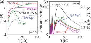
The curves of the total system noise temperature as a function of load resistance for different series capacitances shown in Fig. 6(a) look rather similar to each other since the struggle between and is always comparable - except for pF (solid blue line), where matching is so poor that a significant part of the incoming power is reflected and there is less power transfer to and from circuit and load.
Knowing now the total noise power and the expected signal height, we can calculate and plot the signal-to-noise ratio at a given bandwidth ( in Fig. 6(b)) and the charge sensitivity . While for high losses in the matching network () the SNR barely depends on the series capacitance, decreasing the circuit’s losses to can double it. An important point to note, though, is that values leading to improper matching (in particular , ) can only compete because of the particularly high noise contribution of the matching network. If the total noise is limited by amplifier noise, Fig. 6(a) will essentially be a set of straight lines and Fig. 6(b) will look identical to Fig. 4(d). Nevertheless, we observe that the SNR is not extremely sensitive to the quality of the matching as long as the circuit losses are kept at a moderate level.
It should be mentioned again that the change in reflection coefficient was determined by modeling the QPC with a saddle-point potential which may be inappropriate for actual QPCs in an experiment. Thus the optimal sensitivity might also be attained at much larger QPC resistances where their potential landscape is often found to be more sensitive to local changes. Consequently, the maximal SNR should rather be determined by experimentmueller:10 .
Numerically, we accordingly expect a SNR of the order of 50 at a bandwidth of given a change in QPC conductance of using assumptions realistic for our experimental setup at . This corresponds to a charge sensitivity better than . We will compare these results with experimentally obtained values in the following chapter.
V Measurements on an Etched QPC
To demonstrate the validity of above calculations, we cross-check them against measurements taken with a QPC etched into a shallow two-dimensional electron gas of a GaAs/AlGaAs heterostructure (see Fig. 7). This QPC was designed as a charge detector for electrons trapped in a self-aligned InAs nanowire quantum dotshorubalko:08 . The nanowire was not conductive, though, and therefore we unfortunately could not form a quantum dot. Consequently we will ignore the nanowire’s presence henceforth.
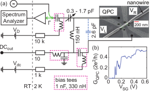
The QPC was incorporated into the matching network as shown in Fig. 7(a). This circuit allows for simultaneous dc measurements and in situ tunability through a variable capacitance (varactor diode), and the values of the circuit parameters correspond to the ones for which the above calculations have been carried out (see Tab. 1).
The conductance through the QPC as a function of side-gate voltage (denoted by and ) is depicted in Fig. 7(b), where a resistance of has been subtracted to compensate for contact and cable resistances. The dc bias applied was . Instead of the monotonous increase in conductance from 0 to with increasing gate voltage expected for a QPC described by a saddle-point potential we observe several transmission resonances and the conductance stays well below over the entire range of applicable gate voltages. These resonances, presumably caused by disorder in the QPC channel, may well influence the shot-noise behavior of our QPC.
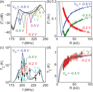
In Fig. 8(a) we demonstrate the tunability of the resonance frequency by applying a reverse-bias voltage to the varactor diode. We clearly see an increase in resonance frequency for larger diode voltages (smaller diode capacitances) and observe a tunability range from roughly 190 to . The background of these curves is set by the frequency-dependent gain of the cryogenic low-noise amplifier in combination with standing waves building up between the matching network and the amplifier input. The magnitude of these standing waves is in agreement with a quoted input standing wave ratio of 1:2.5 of the cryogenic amplifier. Here, the QPC was pinched off completely.
Measuring the reflection at resonance as a function of QPC resistance yields Fig. 8(b). Again, a contact and wiring resistance of has been taken into account. Furthermore, an overall attenuation of (; blue dots), (; green crosses), and (; red circles) has been subtracted from the measured to atone for the attenuators, the directional coupler, losses in the rf lines, standing waves, and the gain of the amplifier, whereafter the result was converted to a linear (voltage) scale. The solid blue, dotted green, and dashed red lines are calculations of at resonance, using , , , , and , (; solid blue line), , (; dotted green line), and , (; dashed red line). We note that the difference in parasitic losses are rather large and non-monotonic, which might stem from a frequency dependence of due to a frequency-dependent fraction of rf current passing the inductance and capacitance. On the other hand, keeping equal for all three calculated curves would move the matched resistances further apart.
Though there are in principle 11 independent parameters in the calculations for Fig. 8(b), knowing and having measured the three resonance frequencies (; ; ) fixes the sum of . From experience and from gauging diode capacitances at low temperatures we have a rather good idea of the values of each of those capacitances. Using these guesses in combination with the position of the minima in we can determine the . Finally, the attenuations are set via the value of for large QPC resistance, and as a a posteriori justification we can compare the results with the background of Fig. 8(a). Thus we feel confident about the appropriateness of the extracted circuit-parameter values.
Figure 8(c) shows the frequency dependence of the total noise in our experimental setup measured with a spectrum analyzer at a resolution bandwidth of and video averaging at . No rf signal was applied, and the QPC was held at a constant resistance of roughly . We converted the measured power spectral density to a noise temperature by subtraction of a frequency-independent gain of and division by the Boltzmann constant.
We observe an unexpectedly high frequency dependence of the noise temperature, accented by spurious noise peaks - marked by black arrows - of unknown originNote5 , changing their magnitude when the diode capacitance is altered. Values of up to 50 K are visible at while the noise temperature is well below above , which necessitates an according choice of resonance frequency when trying to detect single-electron charging. Furthermore, we can see the standing-wave pattern, revealing at which frequencies noise from the QPC and the matching network can couple into the amplifier.
On resonance, the noise level is raised by a few degrees (not regarding the spurious peaks) as expected due to our elevated ambient temperature. A more detailed view of the dependence of the system noise temperature on the matching network is given in Fig. 8(d), where the total noise is plotted as a function of QPC resistance. Here, the resolution bandwidth was reduced to , while the video bandwidth was kept at . By subtracting a gain of (green xs, ) and (red circles; ) the measured curves have been brought to the same level to negate the effect of the spurious noise peaks on the performance at . The calculated curves use the same parameter values as above, including , , , and a dc bias . We also assume a perfectly matched amplifier input.
The circuit temperature of seems somewhat large, but may be explained by poor thermal anchoring of the matching network inside the vacuum cap of the low-temperature stage of our experimental insert.
The system noise is largest for highest load resistances and decreases for lower as power transfer from the matching circuit to the low-noise amplifier - quantified by - is suppressed. We also realize that the exact values of and are not extremely important for the overall system noise (within a certain window), as expected from our considerations in the previous section. Also, our model’s predictions follow the experimental curves rather well, and the subtracted gains are quite plausible.
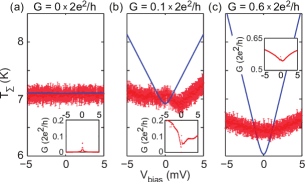
Shot-noise calibration is a very powerful tool for determining system noise temperatures since the noise power of a nanostructure as a function of dc bias can generally be known very accurately. Therefore, we recorded the noise power with a resolution and video bandwidth of and , respectively, as a function of dc bias and show the result for different QPC conductances in Fig. 9. The voltage on the varactor diode was , and we subtracted a gain of . The conductance values chosen were (a), (b), and (c) determined by the current at dc bias (see insets) and taking into account contact and wiring resistances. The error bars denote the statistical spread of repeated measurements.
As expected we do not observe any increase in noise for increasing bias when the QPC is completely pinched off (). For non-zero conductance, though, the bias dependence is much weaker than predicted (with the same parameters as above) and for , the noise is even increasing non-monotonically. Similarly, the dc conductances shown in the insets are not constant. While at bias voltages of several mV we are already well in the non-linear regime, the predictions of Eq. (21) should still hold qualitatively.
A reason why we observe too small values for the shot noise is partially the reflection of incoming signals at the cryogenic amplifier’s input. Roughly of the shot noise may thus be reflected, which, however, still does not fully explain the low observed noise levels at high bias. A further explanation may be an overestimation of power transfer between QPC and amplifier. Additionally, localized states in the QPC leading to the atypical conductance curves in the insets of Fig. 9 and in Fig. 7(b) may strongly influence the shot-noise behavior of the QPC. In particular, it may be conceivable that shot noise is suppressed even at non-integer conductance values since the transmission through the QPC reaches a plateau well before .
Also, our predicted noise temperatures do not exactly match the measured noise at zero bias for high conductance. This most probably stems from the height of the spurious noise peaks in Fig. 8(c) which is found to depend on .
To summarize this experimental section, we can model the system noise in our setup very well with the exception of the unexpected magnitude and shape of the shot-noise curves. Potentially it would be easier to accurately determine the shot noise with a smaller background noise.
With a similar device as the one shown in Fig. 7(a), where the nanowire quantum dot did form, we have obtained a charge sensitivity of approximately , slightly worse than our estimate in Sec. IV. The difference can be attributed to signal loss from standing waves and slightly higher noise in the experimental setup - mainly the matching circuit.
VI Conclusion
In a generally valid derivation for reciprocal two-port networks we have demonstrated a charge-detection experiment’s signal-to-noise ratio to increase linearly with power transfer to the load. Thereby we have found it important that losses in the resonant circuit are minimized, unless shot noise is strongly dominating the overall noise.
Subsequently we have discussed in situ tunability in great detail and have visualized the effect of changing the series capacitance of a circuit. We have also calculated the maximally allowed input voltage and power when limiting the voltage drop over the load, and we have thereby estimated the signal height of the matching network’s response to a change in the charge state of the system to amount to several hundred nV.
By assessing the total noise in the system we could determine the expected overall SNR and charge sensitivity which we found to be only slightly influenced by the exact circuit-parameter values as long as a fair quality of matching is achieved. This fact is substantiated by previous experimentsmueller:10 . The values for the charge sensitivity one can expect in a similar experiment range in a few .
With our present experiments we can confirm tunability and the circuit model as well as the noise levels in the system. We did observe spurious noise peaks in the spectrum, though, which were depending on the circuit impedance. We attributed them to the low-noise amplifier since they occurred also for zero applied rf or dc bias. Furthermore the amount of shot noise we detected was significantly lower than expected. This could partially be explained by the fact that a mismatched amplifier input reflects the noise signal back (on the other hand, this would require higher circuit noise temperatures), and maybe localizations in the QPC - revealing themselves by an unusual gate-voltage behavior and nonlinear characteristics of the QPC - cause the shot noise to be suppressed.
While we still recommend the point of maximal sensitivity to be determined by experiment, our considerations should give an experimentalist dealing with a similar circuit a good feeling for the mutual influences of the circuit elements which is of great importance for optimizing the measurement parameters. Also, in our discussions on the power transfer of noise we identified the parameter relevant for improvement in different regimes.
Since a good power transfer to the charge detector is quite important, it would be very helpful indeed to be able to determine the source of the losses in such a circuit more closely. We believe that such a study would require a detailed analysis - comparable to Ref. hellmueller:12, - of the influence of the exact sample design (e.g. bonding wires, ohmic contacts, distance traveled in the two-dimensional electron gas) on the matching network’s losses.
Acknowledgements
We are greatly indebted to Cecil Barengo and Paul Studerus for their superb technical assistance, and funding by the Swiss National Science Foundation (SNF) via National Center of Competence in Research (NCCR) Nanoscale Science is gratefully acknowledged.
References
- (1) W. Lu, J. Zhongqing, L. Pfeiffer, K. W. West, A. J. and Rimberg, Nature 423, 422 (2003).
- (2) T. Müller, K. Vollenweider, T. Ihn, R. Schleser, M. Sigrist, K. Ensslin, M. Reinwald, and W. Wegscheider, AIP Conf. Proc. 893, 1113 (2007).
- (3) D. J. Reilly, C. M. Marcus, M. P. Hanson, and A. C. Gossard, Appl. Phys. Lett. 91, 162101 (2007).
- (4) M. C. Cassidy, A. S. Dzurak, R. G. Clark, K. D. Petersson, I. Farrer, D. A. Ritchie, and C. G. Smith, Appl. Phys. Lett. 91, 222104 (2007).
- (5) L. Roschier, P. Hakonen, K. Bladh, P. Delsing, K. W. Lehnert, L. Spietz, and R. J. Schoelkopf, J. of Appl. Phys. 95, 1274 (2004).
- (6) R. J. Schoelkopf, P. Wahlgren, A. A. Kozhenikov, P. Delsing, and D. E. Prober, Science 280, 1238 (1998).
- (7) M. A. Sillanpää, L. Roschier, and P. J. Hakonen, Phys. Rev. Lett. 93, 066805 (2004).
- (8) M. A. Sillanpää, L. Roschier, and P. J. Hakonen, Appl. Phys. Lett. 87, 092502 (2005).
- (9) T. Müller, B. Küng, S. Hellmüller, P. Studerus, K. Ensslin, T. Ihn, M. Reinwald, and W. Wegscheider, Appl. Phys. Lett. 97, 202104 (2010).
- (10) A. N. Korotkov and M. A. Paalanen, Appl. Phys. Lett. 74, 4052 (1999).
- (11) D. M. Pozar, Microwave Engineering, 4th ed. (John Wiley & Sons, Inc, 2011).
- (12) K. D. Petersson, C. G. Smith, D. Anderson, P. Atkinson, G. A. C. Jones, and D. A. Ritchie, Nano Lett. 10, 2789 (2010).
- (13) S. Gustavsson, M. Studer, R. Leturcq, T. Ihn, K. Ensslin, D. C. Driscoll, and A. C. Gossard, Phys. Rev. Lett. 99, 206804 (2007).
- (14) R. Q. Twiss, J. Appl. Phys. 26, 599 (1955).
- (15) The sign of determines whether the SNR as a function of is straight, concave or convex.
- (16) W. W. Xue, B. Davis, F. Pan, J. Stettenheim, T. J. Gilheart, A. J. Rimberg, and Z. Ji, Appl. Phys. Lett. 91, 093511 (2007).
- (17) T. Müller, J. Güttinger, D. Bischoff, S. Hellmüller, K. Ensslin, and T. Ihn, Appl. Phys. Lett. 101, 012104 (2012).
- (18) The quality factor of the varactor diode is very large compared to the one of the inductor and we therefore neglect its internal resistance. All losses in the parasitic capacitance can be transformed into ones in series to the inductance without strongly altering the effective values of and if these losses are not significantly larger than the ones from the coil.
- (19) The stray inductances are in the range of a few nH which makes them negligible at frequencies of a few hundred MHz when comparing with impedances of the order of tens of k.
- (20) It should be noted that a larger inductance may lead to a smaller current through the coil and hence a larger value of is needed to account for the same loss of power in the matching network.
- (21) S. Hellmüller, M. Pikulski, T. Müller, B. Küng, G. Puebla-Hellmann, A. Wallraff, M. Beck, K. Ensslin, and T. Ihn, Appl. Phys. Lett. 101, 042112 (2012).
- (22) M. Büttiker, Phys. Rev. B 41, 7906 (1990).
- (23) This may well be inaccurate but our purpose is essentially to have a rough estimate for the change in QPC resistance at a given .
- (24) I. Shorubalko, R. Leturcq, A. Pfund, D. Tyndall, R. Krischek, S. Schön, and K. Ensslin, Nano Lett. 8, 382 (2008).
- (25) V. A. Khlus, Sov. Phys. JETP 66, 1243 (1987).
- (26) With a different amplifier (and a different sample) we did not observe such peaks, but the overall noise level was higher. Using a similar setup, Stettenheim et al.stettenheim:10 observed discrete peaks in their noise spectrum and attributed them to a massive back-action effect through piezoelectric shearing modes of the whole GaAs chip. Since we observe these peaks without any driving power, we can not make such claims.
- (27) J. Stettenheim, M. Thalakulam, F. Pan, M. Bal, Z. Ji, W. W. Xue, L. Pfeiffer, K. W. West, M. P. Blencowe, and A. J. Rimberg, Nature 466, 86 (2010).