A scanning transmon qubit for strong coupling circuit quantum electrodynamics
Main body
Like a quantum computer designed for a particular class of problems, a quantum simulator enables quantitative modeling of quantum systems that is computationally intractable with a classical computer. Quantum simulations of quantum many-body systems have been performed using ultracold atomsbloch2012quantum, and trapped ionsblatt2012quantum, among other systems. Superconducting circuits have recently been investigated as an alternative system in which microwave photons confined to a lattice of coupled resonators act as the particles under study with qubits coupled to the resonators producing effective photon-photon interactionshouck2012onchipquantum, . Such a system promises insight into the nonequilibrium physics of interacting bosons but new tools are needed to understand this complex behavior. Here we demonstrate the operation of a scanning transmon qubit and propose its use as a local probe of photon number within a superconducting resonator lattice. We map the coupling strength of the qubit to a resonator on a separate chip and show that the system reaches the strong coupling regimechiorescu2004coherent, ; wallraff2004strongcoupling, over a wide scanning area.
Over the past decade, the study of quantum physics using superconducting circuits has seen rapid advances in sample design and measurement techniquesschoelkopf2008wiringup, ; clarke2008superconducting, ; martinis2009superconducting, . A great strength of superconducting qubits compared to other promising candidates is that they are fabricated using standard lithography procedures which allow fine tuning of qubit properties and make scaling up the fabrication to devices with many qubits straightforward. Circuit quantum electrodynamics (CQED) is an active branch of quantum physics research in which one or more qubits are strongly coupled to a superconducting coplanar waveguide resonator (CPWR) which is used to control and readout the state of the qubitsblais2004cavityquantum, ; wallraff2004strongcoupling, . A prerequisite for most interesting CQED applications is that the system reach the strong coupling regime in which the rate at which the qubit and the resonator exchange an excitation exceeds the excitation decay rate.
In addition to the CQED architecture’s promise as a quantum computing platform, recent theoretical work has focused on using a CQED lattice, a network of coupled resonators each coupled to its own qubit, as a non-equilibrium quantum simulatorhouck2012onchipquantum, . One particularly interesting prediction for CQED lattice systems is a cross-over from a superfluid-like state to an insulating state as, for example, the coupling between the qubits and their resonators is increasedgreentree2006quantum, ; hartmann2006strongly, ; angelakis2007photonblockadeinduced, , similar to the superfluid-Mott insulator quantum phase transition which has been observed in ultracold atom systemsgreiner2002quantum, ; bloch2012quantum, . More exotic phenomena including analogs of the fractionalhayward2012fractional, and anomalouspetrescu2012anomalous, quantum Hall effects and of Majorana physicsbardyn2012majoranalike, have also been considered. However, while preliminary steps have been taken to build such a CQED lattice systemunderwood2012lowdisorder, , both establishing and probing its expected many-body states remain major experimental challenges.
The simplest method of probing a microwave circuit is to measure transmission between two of its ports. However, in the case of a CQED lattice such a measurement gives only limited insight into the detailed behavior of photons in the interior. Additional information could be obtained by measuring transmission while locally perturbing the interior of the sample, as has been done to image the coherent flow of electrons in two-dimensional electron gas systemseriksson1996cryogenic, ; topinka2000imaging, . This local perturbation requires a new scanning probe tool, such as the one demonstrated here. Besides just perturbing the lattice, a scanning probe qubit can be used to measure the photon number of individual lattice sites following a protocol used to measure photons in non-scannable cavitiesjohnson2010quantum, . One benefit of a scanning qubit in this case is its ability to measure the photon number of interior lattice sites. Measurements of outer resonators, those most easily accessed by a measurement circuit fabricated on the same chip as the lattice, would be difficult to interpret due to edge effects.
While our primary focus is on using the scanning qubit in the context of CQED lattice-based quantum simulation, we note that scanning qubits have been studied previously for other applications. Scanning nitrogen-vacancy (NV) center qubits in diamond have been demonstrated to be sensitive local probes of magnetic fieldrondin2012nanoscale, ; maletinsky2012arobust, . A diamond NV center has also been coupled to a scanning photonic crystal cavityenglund2010deterministic, . While this experiment did not reach the strong coupling regime, the scanning cavity enhanced spontaneous emission from the NV center and allowed its position to be determined with greater spatial resolution.
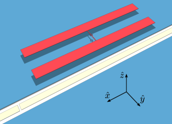
The scanning qubit described here (Fig. 1) is a transmon design consisting of two aluminum islands connected by a thin aluminum wire interrupted by an aluminum oxide tunnel barrierkoch2007chargeinsensitive, . The tunnel barrier provides a large nonlinear inductance, which together with the capacitance between the two islands, makes the transmon behave as a nonlinear LC oscillator whose lowest two energy states can be used as a qubit. The transmon design is well suited for scanning because it couples to CPWRs capacitively and requires no physical connections. The qubit chip was mounted face down to a cryogenic three-axis positioning stage and positioned over a separate chip containing a niobium CPWR with a half-wave resonance at . In order to avoid direct contact between the resonator and the qubit, pads of photoresist thick were deposited on the corners of the qubit chip. The sample holder was mounted to a dilution refrigerator which operated at temperatures .
The main result presented here is the measurement of the strength of the coupling between the resonator and the qubit as a function of qubit position. Following ref. koch2007chargeinsensitive, , the Hamiltonian describing the coupled resonator-qubit system can be approximated by
| (1) |
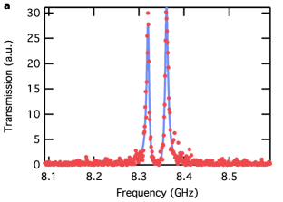
with and the resonator and qubit frequencies respectively. In this expression, are the creation and annihilation operators associated with photons in the resonator and , , and are the Pauli spin matrices associated with the qubit when treated as a two-level system. On resonance , the first two excited states of the system are with corresponding energies above that of the ground state where is the state with photons in the resonator and the qubit in state with () representing the qubit ground (excited) state. When driven with a microwave excitation, transitions to each of these excited states are allowed, resulting in two peaks in the low power transmission spectrum. These peaks are separated in frequency by , called the vacuum Rabi splitting.
The frequency of the resonator depends on its capacitance to its ground plane which is decreased when the qubit chip is brought into close proximity. In order to ensure that resonance was possible at every qubit position, the qubit was fabricated with a pair of tunnel barriers integrated into a loop in place of a single tunnel barrier. By varying the flux through this loop with a magnet coil incorporated into the positioner, the qubit frequency could be varied from a maximum value of to close to zerokoch2007chargeinsensitive, . We note that, although here the flux loop’s only purpose is to make the qubit energy tunable, such a loop can also be operated as a sensitive local magnetometer in a scanning SQUID microscopehuber2008gradiometric, .
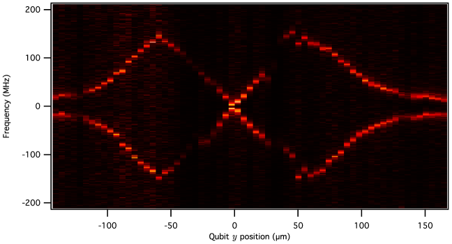
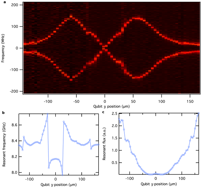
Fig. 2 shows the transmission spectra of the resonator for a sequence of regularly spaced qubit positions along the axis perpendicular to the resonator. At each position, the current through the magnet coil was adjusted to bring the qubit into resonance, where the single transmission peak of the resonator was transformed into two peaks of equal height, clearly demonstrating strong coupling between the scanning qubit and the resonator. The position scan shows two regions of large peak separation symmetric about a position with nearly no peak separation which we set as the origin. In coupling to the resonator the transmon behaves as a dipole antenna. Because the two islands of the qubit are identical, by symmetry no coupling is expected when the qubit is centered above the resonator at . The points of maximum peak separation occur at where one of the two islands is centered over the resonator. At these points, the observed coupling strength was well into the strong coupling regime where the qubit relaxation time was determined by time-domain measurements (see Supplemental Methods) and the photon escape rate was determined from the resonator linewidth. The photon escape rate was chosen to be large in order to increase the rate of data acquisition.
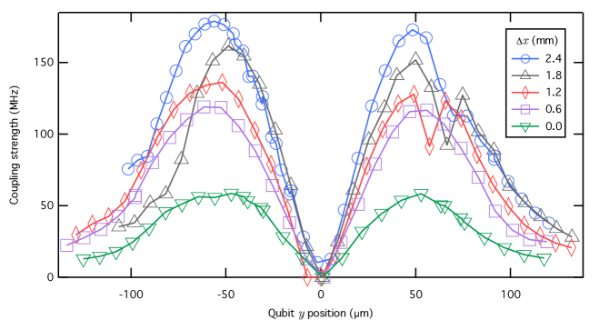
Scans of resonant transmission versus position like Fig. 2 were repeated at five positions along the length of the resonator (the direction) with a spacing of . The coupling strengths extracted from fits to the transmission spectrum at each qubit position are plotted in Fig. 3. The coupling strength increases as the qubit moves from the voltage node at the center of the resonator to the antinode at its end but exhibits the same shape for its dependence at each position.
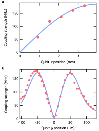
We now consider the data in Fig. 3 more quantitatively. The coupling strength is proportional to the electric field at the position of the qubit when a single photon is present in the resonator. Panel a of Fig. 4 shows the maximum value of for each position along with a fit to the expected sinusoidal dependence of the electric field strength along the direction. The fit provides an absolute reference for the relative positions quoted in Fig. 3. With the position known, we can compare the measurement data with the obtained from finite element simulations (see Supplemental Methods). Panel b of Fig. 4 shows the values of observed for from the resonator midpoint along with the simulation results which show good agreement. The simulation height is somewhat larger than the thickness of the photoresist pads on the corners of the qubit chip but corresponds to a misalignment between the qubit and resonator chips of over the from the edge of the qubit chip to the qubit’s location at the chip center.
In conclusion, we have observed strong coupling between a scanning transmon qubit and a CPWR. Because strong coupling can be reached, anything possible with stationary qubits now becomes possible with a moveable probe opening the door for a wide array of applications in the field of CQED. Such a scanning qubit makes possible quantum measurements of superconducting circuits with spatial resolution. In addition to the scanning measurements of a lattice CQED system discussed earlier, we note that the system studied here demonstrates in situ tuning of the coupling strength which is often a desirable capability experimentally. While the scanning qubit’s coupling can not be tuned on the timescale of the coherence time like some previously demonstrated circuit designsbialczak2011fasttunable, ; srinivasan2011tunable, , it does not require flux or current biasing of the system. For example, for the lattice CQED system mentioned above, a lattice of resonators on one chip could be coupled to a lattice of qubits on a second chip allowing the coupling between each resonator-qubit pair to be tuned together as one chip is scanned over the other. An array of qubits could also be used to measure the statistics of qubit coherence by scanning the qubits one by one across a single measurement resonator.
Methods
The qubit was fabricated using electron beam lithography and double-angle shadow evaporation with controlled oxidation of and layers of aluminum onto a sapphire chip. The crashpads on the corners of the chip were made with photolithography of SU-8 2005 photoresist. The resonator was defined by photolithography and acid etch (, HF, and in a 7.5:4:1 ratio) of a film of niobium on a sapphire chip.
The qubit chip was glued with methyl methacrylate to the tip of a highly conductive copper rod mounted to the cryogenic positioning stage (Attocube ANPx340/RES, ANPz101/RES). The resonator chip was mounted to a copper patterned circuit board with silver paste and aluminum wire bonds which connected the input and output transmission lines to coaxial lines. Wire bonds were only placed around the edge of the chip outside the footprint of the qubit chip. The wiring scheme of the coaxial lines was the same as that described in ref. dicarlo2009demonstration, .
All values of qubit position were determined by potentiometric measurements of resistive position encoders integrated into the positioning stage. Individual position readings had an uncertainty of , and overall the position readings drifted by per . A typical movement of the positioning stage heated the refrigerator from its base temperature of to over . In order to reduce measurement time, most measurements were taken with the refrigerator in the range between and which took only a couple minutes to reach after moving the stage.
Acknowledgements
This work was supported by DARPA under grant #N66001-10-1-4023. DLU is supported by a fellowship from the NSF (DGE-1148900).
Author Contributions
A. A. H. conceived and supervised the experiment. D. L. U. designed and built the sample holder and fabricated the samples. W. E. S. designed and fabricated the samples, performed the measurements and data analysis, and wrote the manuscript. All authors discussed the results and implications and commented on the manuscript at all stages.
Competing Financial Interests
The authors acknowledge no competing financial interests.
References
- (1) Bloch, I., Dalibard, J. & Nascimbène, S. Quantum simulations with ultracold quantum gases. Nature Phys. 8, 267–276 (2012).
- (2) Blatt, R. & Roos, C. F. Quantum simulations with trapped ions. Nature Phys. 8, 277–284 (2012).
- (3) Houck, A. A., Türeci, H. E. & Koch, J. On-chip quantum simulation with superconducting circuits. Nature Phys. 8, 292–299 (2012).
- (4) Chiorescu, I. et al. Coherent dynamics of a flux qubit coupled to a harmonic oscillator. Nature 431, 159–162 (2004).
- (5) Wallraff, A. et al. Strong coupling of a single photon to a superconducting qubit using circuit quantum electrodynamics. Nature 431, 162–167 (2004).
- (6) Schoelkopf, R. J. & Girvin, S. M. Wiring up quantum systems. Nature 451, 664–669 (2008).
- (7) Clarke, J. & Wilhelm, F. K. Superconducting quantum bits. Nature 453, 1031–1042 (2008).
- (8) Martinis, J. M. Superconducting phase qubits. Quantum Inf. Process. 8, 81–103 (2009).
- (9) Blais, A., Huang, R.-S., Wallraff, A., Girvin, S. M. & Schoelkopf, R. J. Cavity quantum electrodynamics for superconducting electrical circuits: An architecture for quantum computation. Phys. Rev. A 69, 062320 (2004).
- (10) Greentree, A. D., Tahan, C., Cole, J. H. & Hollenberg, L. C. L. Quantum phase transitions of light. Nature Phys. 2, 856–861 (2006).
- (11) Hartmann, M. J., Brandão, F. G. S. L. & Plenio, M. B. Strongly interacting polaritons in coupled arrays of cavities. Nature Phys. 2, 849–855 (2006).
- (12) Angelakis, D. G., Santos, M. F. & Bose, S. Photon-blockade-induced Mott transitions and XY spin models in coupled cavity arrays. Phys. Rev. A 76, 031805 (2007).
- (13) Greiner, M., Mandel, O., Esslinger, T., Hänsch, T. W. & Bloch, I. Quantum phase transition from a superfluid to a Mott insulator in a gas of ultracold atoms. Nature 415, 39–44 (2002).
- (14) Hayward, A. L. C., Martin, A. M. & Greentree, A. D. Fractional quantum Hall physics in Jaynes-Cummings-Hubbard lattices. Phys. Rev. Lett. 108, 223602 (2012).
- (15) Petrescu, A., Houck, A. A. & Le Hur, K. Anomalous Hall effects of light and chiral edge modes on the kagomé lattice. Phys. Rev. A 86, 053804 (2012).
-
(16)
Bardyn, C.-E. & İmamoǧlu, A.
Majorana-like modes of light in a one-dimensional
array of nonlinear cavities.
Phys. Rev. Lett. 109, 253606 (2012). - (17) Underwood, D. L., Shanks, W. E., Koch, J. & Houck, A. A. Low-disorder microwave cavity lattices for quantum simulation with photons. Phys. Rev. A 86, 023837 (2012).
- (18) Eriksson, M. A. et al. Cryogenic scanning probe characterization of semiconductor nanostructures. Appl. Phys. Lett. 69, 671–673 (1996).
- (19) Topinka, M. A. et al. Imaging coherent electron flow from a quantum point contact. Science 289, 2323–2326 (2000).
- (20) Johnson, B. R. et al. Quantum non-demolition detection of single microwave photons in a circuit. Nature Phys. 6, 663–667 (2010).
- (21) Rondin, L. et al. Nanoscale magnetic field mapping with a single spin scanning probe magnetometer. Appl. Phys. Lett. 100, 153118 (2012).
- (22) Maletinsky, P. et al. A robust scanning diamond sensor for nanoscale imaging with single nitrogen-vacancy centres. Nat. Nanotechnol. 7, 320–324 (2012).
- (23) Englund, D. et al. Deterministic coupling of a single nitrogen vacancy center to a photonic crystal cavity. Nano Lett. 10, 3922–3926 (2010).
- (24) Koch, J. et al. Charge-insensitive qubit design derived from the Cooper pair box. Phys. Rev. A 76, 042319 (2007).
- (25) Huber, M. E. et al. Gradiometric micro-SQUID susceptometer for scanning measurements of mesoscopic samples. Rev. Sci. Instrum. 79, 053704 (2008).
- (26) Bialczak, R. C. et al. Fast tunable coupler for superconducting qubits. Phys. Rev. Lett. 106, 060501 (2011).
- (27) Srinivasan, S. J., Hoffman, A. J., Gambetta, J. M. & Houck, A. A. Tunable coupling in circuit quantum electrodynamics using a superconducting charge qubit with a V-shaped energy level diagram. Phys. Rev. Lett. 106, 083601 (2011).
- (28) DiCarlo, L. et al. Demonstration of two-qubit algorithms with a superconducting quantum processor. Nature 460, 240–244 (2009).
Supplementary Methods
Fitting functions
Non-linear least-squares fitting routines were used to determine the coupling strength from transmission data and to produce the curves shown in Fig. 4. Here we briefly describe the functions used in each case.
Transmission measurements
Transmission measurements were made in the low power limit for which the rate of photons entering the resonator was less than the escape rate, so that the resonator occupancy was less than one photon on average. In this case, the transmission spectrum contains peaks at frequencies corresponding to transitions from the ground state to the states and which possess a component and are located at energies and above the ground state. The states and their frequencies are found by diagonalizing the Hamiltonian given in equation (1):
and
| (S1) |
with . The peak amplitudes are proportional to the probabilities of a photon being measured in the states . The peak linewidths are equal to the decay rates of the qubit () and the photon () weighted by the probability of measuring a qubit excitation and a photon respectively: . We take transmission peaks as following a lorentzian lineshape and use the following form to fit the resonator transmission:
| (S2) |
where is the overall amplitude accounting for all attenuation and amplification in the measurement circuit, is the background of the detector, and is the complex lorentzian centered at with width :
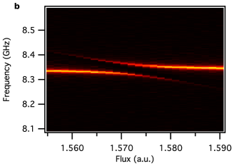
When fitting for , the parameters , , , , , and were allowed to vary, while was held fixed to the value obtained from coherence measurements. Fig. S1 shows the result of fitting one of the transmission spectra from Fig. 2. Also shown is a plot of transmission versus flux as the qubit passes through resonance. For the coupling strength values shown in Fig. 3, similar flux scans were taken and the plotted values of coupling strength were obtained by averaging the coupling strength values obtained from fitting the transmission at each flux value.
Coupling strength versus
The voltage profiles of the modes of a CPWR with open boundary conditions are sinusoidal along the length of the resonator with antinodes at its ends. The coupling strength is proportional to the resonator voltage with one photon present and so should follow this sinusoid. The maximum coupling strength at each position shown in panel a of Fig. 4 was fit to the sinusoidal form:
| (S3) |
where is the resonator length and and were the fitting parameters. Here is the set of displacements in from the first position (i.e. the values are ; ; ; etc.). In panel a of Fig. 4, the measured coupling strengths and the fit are plotted versus .
Coupling strength versus
In order to perform the fit of coupling strength versus shown in panel b of Fig. 4, the following expression for the coupling strength given in ref. koch2007chargeinsensitive, was used:
with the characteristic line impedance taken to be and the sinusoidal mode shape factor given in equation (S3). In order to describe the voltage division factor and the transmon matrix element , we first define to be the capacitance between components and and label the components of the system with and for the two islands of the transmon, for the resonator center pin, and for all other pieces of metal (the two ground planes and the metal frame on the qubit chip). The voltage division factor gives the fraction of the voltage drop from the resonator center pin to ground that falls across the two islands of the qubit. It can be written in terms of capacitance coefficients as
where . We find the matrix element by numerically diagonalizing the transmon Hamiltonian given in ref. koch2007chargeinsensitive,
to finds it eigenstates and eigenenergies and then evaluating , where and are the eigenstates with the two lowest energies, and . The charging energy used in the calculation was calculated using the total capacitance given by
The qubit frequency is given by and is thus a function of and . In calculating , was numerically inverted to solve for with set equal to since measurements of the coupling strength were made with the qubit close to the resonator’s frequency.
In order to produce the fit shown in panel b of Fig. 4, the coupling strength was calculated using the known values of and , the value of obtained from the fit in panel a of Fig. 4, and the values of the capacitances found by finite element analysis for a grid of and values with spacing. The measured coupling strength versus was fit to the found by interpolating between the and grid points with as the only free parameter. The finite element simulation was then repeated with the fitted value of in order to produce the curve shown in panel b of Fig. 4. We note that at the fitted value of the charging energy is similar to values used in other CQED experiments and corresponds to a ratio of , within the transmon regime where the offset charge across the transmon islands (not included in the Hamiltonian given above) may be ignored.
By the use of alignment marks on the resonator and qubit chips, it was possible to confirm that the misalignment between the two chips was . A misalignment of was used in the finite element calculations for the capacitance coefficients. Using a misalignment of () instead gave a the fitted height of ().
Coherence measurements
Qubit coherence times (, ) were obtained using the techniques described in ref. schreier2008suppressing, . The measurements were made during the same cooldown and at the same position as the data shown in Fig. 2. For technical reasons, the measurements were made immediately after the refrigerator was warmed up to and then cooled back down to its base temperature. The coherence measurements were performed at () in Fig. 2 with the qubit frequency detuned below the resonator.
Supplementary Discussion
Here we provide some additional measurements and analysis related to scanning the qubit over the resonator. In Fig. 2, the transmission is suppressed near and due to the resonator’s coupling to spurious modes. Because the behavior of these modes is symmetric in qubit position, we believe them to be caused by resonances between the resonator chip and a layer of metal on the qubit chip that was patterned symmetrically. The extra metal on the qubit chip was deposited for technical reasons and is not needed for the functioning of the qubit. By redesigning the qubit chip or resonator chip, these modes could be eliminated.
In panel a of Fig. S2, the data from Fig. 2 is replotted after removing the background and normalizing the transmission peaks to unity in order to make the peaks near and more visible. In Fig. 2, the origin of the frequency axis was set to the location of the high power transmission peak and the qubit frequency was tuned to produce two peaks of equal height in transmission. For some positions near where the resonator coupled to the spurious modes, these conditions produced two peaks not centered around zero. In panel a of Fig. S2, the frequency axis at each position has been shifted to center the peaks around zero, so that the transmission peaks at neighboring positions can be more easily compared.
The spurious modes appeared as lower and broader peaks in transmission at frequencies that varied with position and did not vary with magnetic flux. These modes were always present but only affected the measurement of the resonator-qubit system when their frequencies were close to the resonator frequency. When the frequency of one of these modes was close to the resonator frequency, the coupling between the spurious mode and the resonator resulted in two modes with excitations partially of the resonator and partially of the spurious mode. The narrower peak of the resulting two peaks in transmission was chosen to be the resonator peak for the purpose of coupling to the qubit. Panel b of Fig. S2 shows the frequency of the chosen peak for each position in Fig. 2. Jumps in the resonator frequency due to avoided crossings with spurious modes are visible at the positions with low transmission in Fig. 2.
The scan shown in Fig. 2 was taken on a separate cooldown from the scans shown in Fig. 3. The same resonator and qubit samples were used for both sets of measurements, but the sample stage was disassembled in between the cooldowns. During the cooldown in which data in Fig. 2 was taken, the qubit’s position was not varied, so the absolute position of the data is not known. However, using the maximum value of from Fig. 2 and the curve shown in panel a of Fig. 4 to calibrate the position, one finds the data in Fig. 2 was taken at .
Changing the position of the qubit also affected the threading of flux through the qubit’s SQUID loop. Once the SQUID loop was moved away from the gaps in the coplanar waveguide and positioned above the superconducting ground plane, the amount of flux produced by the magnet coil required to tune qubit into resonance increased rapidly because the Meissner effect screened the magnetic field away from the superconducting ground plane. In panel c of Fig. S2, the coil magnetic flux that brought the qubit into resonance with the resonator is plotted for each position of Fig. 2. The impact of the magnetic field screening could be greatly reduced by fabricating holes in the resonator’s ground plane.
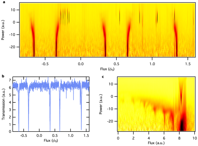
The strong dependence of the resonant magnetic flux on the qubit position as well as the steepness of the slope of qubit frequency versus magnetic flux (maximum qubit frequency ) necessitated careful flux scanning at each qubit position in order to locate resonance. Searching for resonance by monitoring the transmission spectrum for an avoided crossing feature like the one shown in panel b of Fig. S1 would have required a long measurement time at each qubit position. Instead, only the low power transmission at the frequency of the high power transmission peak was monitored as the flux was swept.
When , one of the two mode frequencies given in equation (S1) differs from by and is associated with a large peak in transmission. For most qubit frequencies this frequency shift is small compared to the resonator linewidth and so transmission at is high. However, when , the mode frequencies are shifted from by and transmission at is low. Panel a of Fig. S3 illustrates this behavior by showing showing transmission at versus flux and input power. Regular dips in transmission occur at low power where the qubit passes through resonance. Panel b of Fig. S3 plots just the low power transmission versus flux and shows that resonance can be easily identified by monitoring transmission at just one frequency value. In practice, a scan like that shown in panel b was taken at each position to identify the resonant flux range, and then a scan like that shown in panel b of S1 was taken over this flux range to obtain transmission spectra to fit for .
Additional features are present in the crossover from the low power region to the high power region of the transmission. Panel c of S1 shows a finer scan of transmission versus power and flux at a qubit position close to that of the scan in panel a. These features are likely related to higher level qubit transitions coming into resonance with the resonator, though additional analysis is needed.
In the main text, results have been presented for the coupling of the qubit to the resonator as a function of lateral position ( and ). Measurements of the coupling’s dependence on the qubit’s vertical displacement from the resonator were not possible due to misalignment between the resonator and qubit chips. Evidence of this misalignment is visible in panel a of Fig. S3 which plots the resonator frequency versus the positioner’s reading denoted by . The origin of was chosen to be the point at which the positioner could no longer advance due to contact with the resonator chip. Above , the resonator frequency is shifted to higher values as the qubit chip is brought closer as expected due to the modification of the resonator’s effective dielectric constant by the qubit’s presence. Below , the resonator frequency’s dependence on weakens and disappears even as the positioner continues to move. We interpret this behavior as the qubit chip coming into first partial contact with the resonator and then nearly full contact as compliance in the sample holder allow the two chips to align. We attribute the relatively small magnitude of the discrepancy of the qubit height obtained by the fit shown in Fig. 4 from the height of the photoresist pads to this compliance in the sample holder.
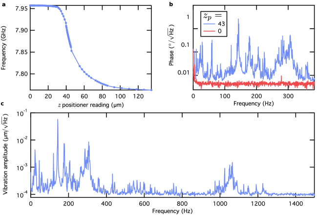
We note that the shift of the resonator frequency due to the qubit chip shown in panel a of Fig. S4 demonstrates the possibility of using a scannable chip to produce a defect in a CQED lattice by shifting the frequency of one of the resonators within the lattice. For scanning experiments where no defect is desired, the shift shown in panel a could be made unimportant by scanning with a chip larger than the entire CQED lattice. In this case, the resonator at each lattice site would receive the same shift.
The resonator frequency’s dependence on the qubit chip height shown in panel a of Fig. S4 allowed the resonator to be used to measure the qubit height. Panel b of Fig. S4 plots noise spectra of the transmitted phase at the resonator frequency when the qubit chip is at and . We interpret the phase fluctuations present when the qubit chip is hovering above the resonator and not present when the qubit chip is in hard contact as being due to motion of the qubit chip relative to the resonator chip. Using the resonator’s phase versus frequency curve to convert the phase noise into an effective resonator frequency noise and then the curve shown in panel a of Fig. S4 to convert frequency into position, we obtain the position noise spectrum shown in panel c of Fig. S4. Repeating this procedure at another position and using the amplitude noise instead of the phase noise resulted in vibration spectra with similar features at similar magnitudes, confirming the interpretation of the features as being due to vibration of the qubit chip. The spectrum shown in panel c of Fig. S4 is typical for the mechanical response of cryogenic positioners such as those used in this experiment. The motion of the refrigerator base plate inferred from the spectrum shown in panel c of Fig. S4 agreed with measurements made with an accelerometer of another refrigerator that was the same model as that used for the measurements presented here. Because all measurements of the qubit were made with the resonator and qubit chips in hard contact, no vibration isolation elements were included in the sample holder. In order to measure the dependence of the qubit-resonator coupling on height, such vibration isolation would need to be considered in addition to the alignment of the qubit and resonator chips.
References
- (1) Schreier, J. A. et al. Suppressing charge noise decoherence in superconducting charge qubits. Phys. Rev. B 77, 180502 (2008).