Integrated Optical Dipole Trap for Cold Neutral Atoms with an Optical Waveguide Coupler
Abstract
An integrated optical dipole trap uses two-color (red and blue-detuned) traveling evanescent wave fields for trapping cold neutral atoms. To achieve longitudinal confinement, we propose using an integrated optical waveguide coupler, which provides a potential gradient along the beam propagation direction sufficient to confine atoms. This integrated optical dipole trap can support an atomic ensemble with a large optical depth due to its small mode area. Its quasi- waveguide mode has an advantage over the mode of a nanofiber, with little inhomogeneous Zeeman broadening at the trapping region. The longitudinal confinement eliminates the need for a 1-D optical lattice, reducing collisional blockaded atomic loading, potentially producing larger ensembles. The waveguide trap allows for scalability and integrability with nano-fabrication technology. We analyze the potential performance of such integrated atom traps.
1 Introduction
Optically trapped neutral atoms have been used for precision quantum metrology [1] and quantum information processing [2, 3] because a neutral atom is an excellent frequency reference and atoms trapped in a far-off resonant optical field have a long coherence time and a long lifetime. There is a wide variety of free-space configurations that have been employed to optically confine neutral atoms. Free-space optical dipole traps [4] confine a cigar-shaped atomic cloud with a tightly focused traveling wave, creating harmonic potentials along the propagation direction and transverse directions. To enhance longitudinal confinement, a 1-D standing wave potential (optical lattice) [5] can be used, creating an array of small-volume trapping sites. Atoms trapped in 2-D or 3-D optical lattices are exploited to model quantum many-body systems in periodic potentials and study fundamental condensed-matter problems [6, 7, 8]. The two-color evanescent light surface trap by total internal reflection at the surface of a dielectric material was proposed in 1991 [9] and realized in 2003 [10, 11] on the surface of a prism. Recent work trapping atoms with light guided in optical fibers includes a hollow-core photonic crystal fiber dipole trap [12, 13] and nanofiber 1-D optical lattices with two-color evanescent fields [14, 15]. An addition to trapping atoms, guided optical modes are also being investigated for trapping and manipulating nanoparticles and biomolecules in microfluidic slot-waveguide geometries [16] and in the evanescent field of tapered optical fibers [17].
Advances in optical waveguide technology suggest that developing atom traps based on waveguides may provide an interesting platform for quantum information processing and sensing, building on the scalability inherent in waveguide fabrication that may allow networks and integration that would be difficult with free-standing optical fibers. Using optical waveguides along with 1-D optical lattices has been proposed to trap neutral atoms with two-color evanescent fields [18, 19]. Here we propose a design that provides longitudinal confinement without resorting to 1-D lattices, creating a trap similar to the workhorse optical dipole trap, but integrated on a surface rather than in free space.
The integrated optical dipole trap (IODT) with an integrated optical waveguide coupler (IOWC) creates a small mode area resulting in a potentially large optical depth of an atomic ensemble, which determines e.g., the performance of quantum memory based on electromagnetically induced transparency (EIT) [21, 20, 22] or the phase sensitivity of atomic spin polarization spectroscopy [23, 24]. The small mode volume allows for a low optical power to trap atoms. In addition, the high optical depth creates a strong atom-light coupling, and the IODT with an integrated Bragg-grating cavity may additionally increase the optical depth according to its cavity finesse. A nanofiber-based Bragg-grating cavity has been explored and demonstrated [25, 26], an interesting cavity QED (quantum electrodynamics) system [27, 28] nearing the single-atom strong coupling regime. Cavity QED with an atomic mirror created with periodically trapped atoms was also proposed [29]. The IODT can operate with the same laser wavelengths as a nanofiber trap to allow a state-insensitive trap (for 133Cs) that can improve the lifetime and coherence time of trapped atoms [30, 31, 32].
The IODT with two-color traveling evanescent wave fields uses differential decay lengths of a blue and a red-detuned evanescent fields to trap atoms along the transverse direction similar to the nanofiber’s radial atom confinement. In addition, the advantage of geometrical design of the IODT, such as an integrated optical waveguide coupler, creates a sufficient potential gradient along the propagation direction, which can confine atoms along that direction, obviating the need for a standing wave which is required for the axial confinement of the nanofiber atom trap. This should improve the loading efficiency over a nanofiber trap, where the optical lattice site volume results in inefficient, collisionally blockaded atomic loading [33] of 0 or 1 atom per lattice site.
In addition, using the quasi- mode of the IODT trap, we can make a stable trap perpendicular to the input polarization, where there is no longitudinal component and no ellipticity at the trapping region. Nanofiber atom traps with the mode usually create radial atom confinement using azimuthal symmetry breaking in the strongly guided regime where there exists more evanescent field parallel to the input polarization, but it has a non-negligible longitudinal component at its trapping region.
The IODT leveraged by nano-fabrication technology has the possibility of being scalable and integrated for a large scale quantum memory and multiple arrays of atomic magnetometry sensors. The structural robustness and heat transfer of an IODT are much better than the nanofiber because of its substrate and nano-fabricated structure, allowing for higher optical powers and deeper traps.
2 Trapping Atoms
The IODT creates optical potentials that confine atoms along the transverse directions with the differential decay lengths of two-color traveling evanescent wave fields and confine atoms along the propagation direction with a sufficient potential gradient created by the geometrical design of the IODT. The IODT optical trap works in a similar manner as an optical dipole trap. For a single atomic transition (), the induced light shift (AC Stark shift) creates an optical potential. This potential [4] for a large detuning () is
| (1) |
where is the laser intensity, and is the spontaneous decay rate of the excited state. A blue-detuned trapping beam creates a repulsive potential (), and a red-detuned trapping beam produces an attractive potential (). For trapping near ( nm) the surface of a dielectric, the blue-detuned beam needs to compensate the attractive van der Waals potential (the Casimir-Polder interaction is negligible around the trapping region [34]). Approximating the surface to be an infinite dielectric, the van der Waals potential is
| (2) |
where is the dielectric permittivity, is the distance from the waveguide surface, and is determined from atomic dipole transition [18, 35]. The total potential along the vertical direction of the waveguide is
If the chosen wavelengths are near to other atomic transitions, the optical potential can be generalized by summing the light shifts for each laser over each transition. We use as an example optical trapping of cold 87Rb atoms in their ground-state manifold 5S1/2 with two excited-state manifolds of 5P1/2 and 5P3/2 as
| (4) |
We can trap cold neutral atoms using single blue-detuned and single red-detuned traveling evanescent waves of the IODT, as the IODT has a potential gradient along the propagation direction similar to an optical dipole trap without standing waves. The IODT design can easily be generalized for trapping other atomic species, with dimensions appropriately scaled to the relevant trapping laser wavelengths.
3 Vector Light Shift of Trapping Beams
The atom-light interaction is generally described with scalar, vector, and tensor light shifts [24].
where , is a light polarization, is the total angular momentum operator, the tensor coefficients are calculated from Wigner-Eckart theorem, an is the characteristic polarizability of atomic transition from (lower level) to (upper levels). The scalar light shift () yields the trapping of atoms with an optical dipole trap. Vector () and tensor () light shifts depend on the polarization state of light and populated magnetic sublevels for a given quantization axis. For example, when the propagation direction of light and the populated atomic state are colinear along the quantization () axis, the vector light shift (, where is Stokes vector components [36]) is proportional to the ellipticity of the light. For nanofiber atom traps, the suppression of vector light shifts from trapping beams is important due to the longitudinal component at the trapping region. The vector light shift induces a state-dependent light shift and a fictitious magnetic field, which can make magnetometry and Faraday rotation measurements challenging. State-insensitive traps [30, 31] can have long lifetimes and coherence times, by matching the potential curvatures of the ground and excited state atoms (including Zeeman sublevels) with a properly chosen two-color magic wavelength trap.
For the ground state () of alkali atoms in the far-detuned regime where (excited-state hyperfine splitting), the sums of tensor light shifts are cancelled for and transitions. The sums of tensor light shifts from the excited-state hyperfine transition to all upper transitions do not completely cancel, but are an order of magnitude smaller than vector light shifts, and thus can be neglected.
A state-insensitive, compensated nanofiber trap was proposed and demonstrated for atoms with a two-color magic wavelength atom trap and the cancellation of vector light shifts of a forward propagating blue-detuned light by means of adding a backward propagating off-resonant blue-detuned beam [31, 32]. In the nanofiber’s strongly guided regime (), a quasi-linear mode’s electric field parallel to the input polarization generates larger evanescent fields, which a nanofiber-based 1D lattice exploits, but has a non-negligible longitudinal component () due to the discontinuity of electric field and azimuthal symmetry breaking. The orthogonal linear polarization of blue and red fields has been also demonstrated in a nanofiber [15]. The trapped atoms in the hyperfine ground states experience no longitudinal component along the radial and axial directions, but the trapping potential in the azimuthal direction experiences vector light shifts and inhomogeneous Zeeman broadening [32].
In the case of the rectangular waveguide (see Fig. 3), the fundamental mode is a quasi- mode, which also has an electric field along the input polarization like the mode. However, unlike mode, the waveguide has a large evanescent field perpendicular to the input polarization because of its thin height in addition to a higher index of refraction. Therefore, we can have optical potentials of blue and red-detuned light along the direction perpendicular to the input polarizations with moderate optical powers. Furthermore, the waveguide can decouple the azimuthal noise in the trap potential compared to the nanofiber traps [15, 32], and inhomogeneous Zeeman broadening and the vector light shift is suppressed.
Waveguide atom trapping with the quasi- mode has the advantage of virtually no vector light shift at the atom trapping region because the quasi- mode’s evanescent field perpendicular to the input polarization has a very small component. At the potential minimum, the waveguide mode has of less than 0.3 %, ten times less than a nanofiber trap. Even in the motional ground state of the transverse direction (x-axis, assuming a harmonic trap with the trap frequency 280 kHz) the atoms can experience an inhomogeneous broadening due to the vector light shift, but for reasonable trapping parameters, the broadening is small (0.1 %). The longitudinal component mostly comes from two side edges of the waveguide cross-section, and may be further decreased by redesigning the waveguide’s width within the condition of single-mode operation.
4 Waveguide Design
The optical waveguide is designed for efficient atom trapping with low insertion loss at both operating wavelengths (760 nm and 1064 nm for 87Rb atoms), while satisfying straightforward operation and noncritical design criteria that facilitate the design/fabrication process. Various types of integrated optical waveguide structures, such as rib, ridge, pedestal, strip, trapezoid, and nanoslot, can be used for the atom trapping. Here, CMOS-compatible Si3N4 strip-loaded optical waveguide on silicon on insulator (SOI) is considered because of relatively low loss at the operating wavelengths, low coupling loss, and a large evanescent field caused by weak optical guiding, compared to Si or GaAs waveguides.
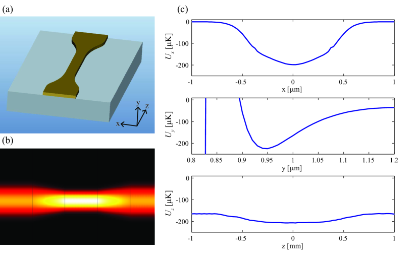
One may think of an hourglass shape of strip-loaded optical waveguides (see Fig. 1 (a)) in order to reduce the optical potential at the ends to provide longitudinal confinement. This does not, however, create a sufficient potential gradient along the propagation direction to achieve the desired device performance (see Fig. 1 (c)). Simply splitting each input and output port into two optical waveguides, a well-known waveguide coupler configuration, allows a much larger extinction ratio along the propagation direction and a 3 dB power reduction in each waveguide caused by spatial separation of optical fields into two transverse directions. Smaller separation between the ports is better for adiabaticity, but separation of less than 1 m leads to an insufficient potential gradient along the propagation direction due to the residual light between two ports. High refractive index material such as silicon or III-V compounds might be used in the form of a strip-loaded waveguide or a nanoslot [37], which requires a large index difference to induce intense evanescent fields. However, special care should be taken to choose an operating wavelength and its polarization for both low optical loss and no ellipticity. Organic polymer materials are also good candidates because of their intrinsic properties such as low optical loss, weak dispersion, and low refractive index. Polymers can be molecularly engineered to have nonlinearity for active device applications controlled by electrical and optical signals, which may allow for additional device functionality.
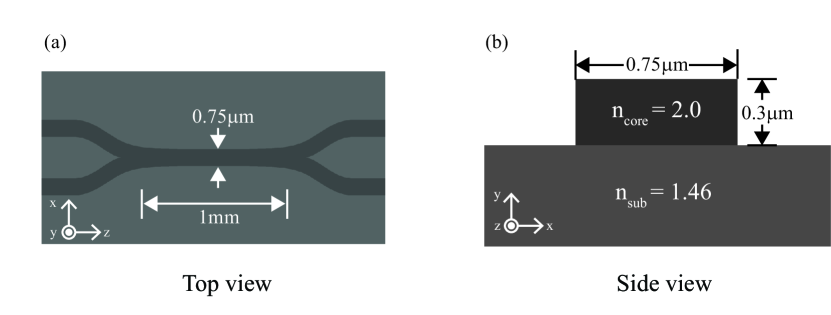
The waveguide is constructed with a silicon nitride core (Si3N4, n) and a silicon oxide substrate (SiO2, n1.46) as shown in Fig. 1. Si3N4 can be grown by various types of deposition techniques, such as plasma enhanced chemical vapor deposition (PECVD) and inductively coupled plasma (ICP), and its refractive index is controllable in the range of . The core size of the waveguide at the center of the IOWC is 750 nm 300 nm (see Fig. 2). The length of the core waveguide is designed to be 1 mm, but may be longer depending on applications and lithographical capability.
The waveguide is designed for atom trapping and single mode operation so that only the quasi- mode can propagate along the waveguide at both operating wavelengths. For this design, we consider how to obtain an intense evanescent field while maintaining the single mode operation and high optical coupling efficiency. As the height of waveguide decreases, more evanescent field can be obtained for a small mode area, resulting in lower power requirements for the same depth trap. However, when the height of the IOWC is smaller than nm, the ideal convergence condition of the 1064 nm waveguide modes is not satisfied. We choose a 300 nm thick waveguide to allow nm design uncertainty. The width of the waveguide can be similarly treated. As the width diminishes, the evanescent field intensifies due to the reduced mode area. We note that improper height and/or width can cause multi-mode interference (MMI) or poor optical coupling efficiency. Our waveguide design is optimized for guiding 760 nm and 1064 nm trapping lasers (see Fig. 2). We choose a 750 nm width to prevent MMI in the IOWC. This sub-micron width design needs only a few mW of optical power of 760 nm and 1064 nm trapping light to produce useable trap depths because of the small cross-sectional area. In contrast, a few m beam diameter of an optical dipole trap requires a few hundreds of mW of optical power for the same blue- and red-detuned trapping lasers due to its large mode area. Of course, the width of the IOWC can be adjusted to vary the trapping volume. For a large trapping volume, which may be useful to increase the number of trapped atoms, we may need to increase optical powers and to consider the MMI condition carefully. The IOWC is formed to include an adiabatic region in the coupling sections for a single mode operation and low bending loss.
5 Simulations
We simulated the 3-D structure of the IODT with the IOWC using FIMMWAVE based on the FMM (Film Mode Matching) method that numerically calculates a 2-D mode along the beam-propagation direction [38, 39]. The 2D cross-sectional views of two waveguide modes (760 nm and 1064 nm) that can trap atoms near the surface are shown in Fig. 3. The blue-detuned potential (760 nm) is required to compensate the attractive van der Waals potential. The different field decay lengths of 760 nm and 1064 nm evanescent fields create an optical potential to trap atoms at a distance of nm above the waveguide (see of Fig. 4(c)).
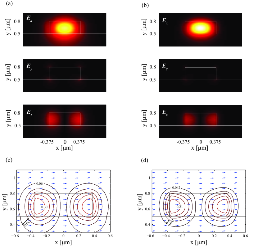
The waveguide designed for single mode operation has only the quasi- mode at both operating wavelengths. The quasi- mode contains strong (horizontal electric field) and weak and modes around the corners of the waveguide as shown in Fig. 3. Therefore, at the region where the atoms are trapped, nm above the central surface of IOWC, there exists negligible and fields. Compared to the nanofiber trap using the mode’s electric field parallel to the input polarization, the proposed device has a negligible polarization ellipticity (see Fig. 3 (c), (d)) at the trapping area along the direction perpendicular to the input polarization.
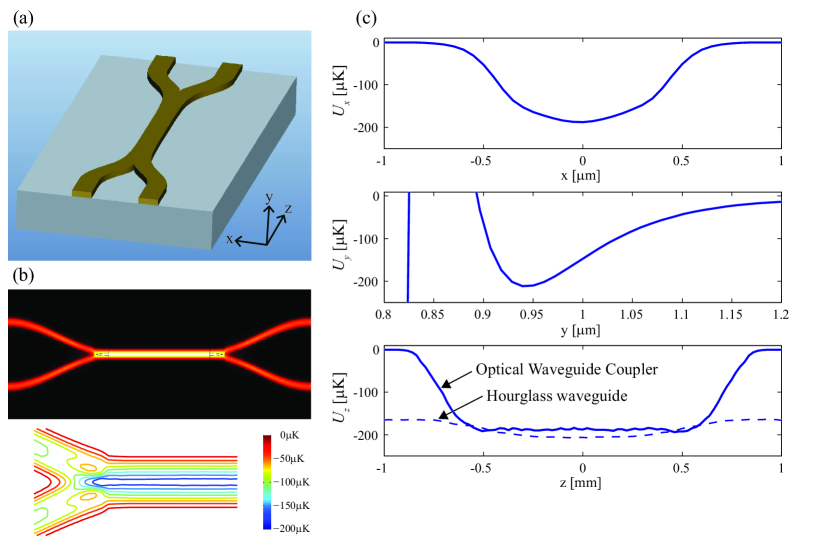
The trapping potentials along the transverse ( and ) and the propagation () directions are calculated (see Fig. 4(c)). The optical potential gradient confines atoms along the propagation direction. Nanofiber-based traps require standing waves for confining atoms along the propagation direction, but the IODT with the IOWC can use only two-color traveling evanescent waves due to its geometry. The trapping potentials (, , ) at the central trapping region of the waveguide are about (see Fig. 4) for and . With a minimal height of the IOWC ( nm), the required optical powers of trapping beams can be further reduced by a factor of two, but we chose the values considering the convergence of the waveguide modes. Trapping frequencies can be estimated using the harmonic trap approximation as . The trap frequencies along the transverse direction are (see Fig. 4).
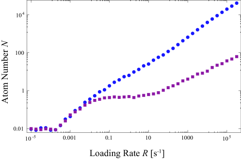
The IODT with no required 1-D optical lattice can eliminate the collisional blockade regime that limits the average number of trapped atoms per lattice site to 0.5 (see Fig. 5). (Collisional blockade arises from two-body collisions that create very high atom-loss rates for lattice sites with more than one atom. A recent experiment [40] shows that filling factor can be improved to 0.8 beyond the 0.5 limit using blue-detuned light-assisted collisions.) We expect that an IODT could sustain more atoms than the nanofiber-based 1-D optical lattices due to reduced two-body collisions, but the number the trapped atoms needs to be carefully determined in the experiment. The decay process of the trapped atoms is modeled with atomic loading rate (), the background gas collision (), and light-assisted two body collisions () as follows:
| (6) |
We estimated the light-assisted two-body collision rate for the IODT with the IOWC () and the nanofiber-based 1-D optical lattices () considering an effective trap volume, [41]. The atomic loading process from magneto-optically trapped (MOT) atoms to an optical dipole trap needs a near-resonant MOT beam to provide cooling in the potential. This produces excited-state atoms, and thus light-assisted two body collisions. Dominated by a radiative escape process, the collision rate depends on the intensity, detuning, and duration of the near-resonant beam [40, 42, 43]. The trap volume of the IODT with the IOWC is a few thousand times more than that of the 1-D optical lattice site. Therefore light-assisted two body collisional loss is reduced for the IODT, and we may avoid a collisionally blockaded loading process [33, 44].
The loading efficiency of the nanofiber-based optical lattices is lower than that of the IODT case due to , but during an adiabatic loading procedure, a recapturing process [42] by the near-resonant MOT beam can enhance the atom loading into the 1-D array of single atom traps. After turning off the adiabatic loading, the single atoms trapped in the nanofiber optical lattices have no more two-body or three-body collisions. Without the presence of near-resonant light, the collision rate in an IODT will be dominated by three-body loss, but this should be negligible at expected densities. A near-resonant probe for an absorption measurement can induce light-assisted collisions (two-body loss) and light-induced heating of the atoms (effectively a one-body loss mechanism). Those could however be greatly suppressed with an off-resonant probe () for a phase-shift measurement. A detailed comparison of atom number between a nanofiber trap or an IODT with the IOWC is somewhat difficult. The total number of trapped atoms is determined by the initial density of MOT cloud, the efficiency of adiabatic loading process from MOT atoms to the optical trap, two-body collision rates with a given trapping volume, and the intensity, detuning, and duration of the near-resonant MOT beam (or probe beam for each measurement protocol).
One additional possible advantage of the IODT over the nanonfiber trap is potentially reduced phase fluctuations. It is thought that phase fluctuations of the 1D lattice due to spontaneous Brillioun scattering limits the lifetime of trapped atoms on the nanofiber traps. By eliminating the lattice, one eliminates the sensitivity to phase fluctuations.
6 Conclusion
An atomic ensemble with a large optical depth stored in an IODT provides a versatile and scalable tool for a variety of quantum information applications, including quantum memory, quantum repeaters [45] and magnetic sensors based on atomic spin polarization spectroscopy. As an example, EIT-based quantum memory in a system enables us to store a signal photon pulse in the collective atomic ensemble as a photonic dark state polariton [20], using a classical control field that induces slow light, and later retrieve the signal photon from the atomic medium with the control field. The efficiency of the quantum memory depends on the optical depth of the atomic medium. The IODT has a high optical depth due to the small-mode volume, and the output photon is automatically guided and hence can be used with high efficiency. Therefore, we can use this as a scalable and integrable quantum memory unit.
As a second example, the waveguide can be used for atomic spin polarization spectroscopy [23, 24]. The quasi- mode’s electric field perpendicular to the input polarization has no longitudinal component at the trapping region. Therefore, the trapping beams do not induce vector light shifts, and the vector light shift of a linearly polarized off-resonant probe for Faraday measurement is not limited by the trapping beam’s vector light shift.
Therefore, the IODT has the potential to be a compact and robust atomic magnetometry sensor, with less need to develop schemes to cancel vector light shifts.
The integrated optical dipole trap (IODT) with an integrated optical waveguide coupler (IOWC) can trap cold neutral atoms near the surface with two-color traveling evanescent wave fields. The proposed structure of the IOWC creates a confining potential along the propagation direction without optical lattices or standing waves. Because of the small mode volume, the IODT can produce a high optical depth of an atomic ensemble, the figure-of-merit for the performance of quantum memory or an atomic magnetometry sensor. The scalability and integrability of the IODT are promising for a large scale quantum memory or a multiple-array of atomic magnetometry sensors. The IODT eliminates collisionally blockaded atomic loading and thus may have a better loading efficiency than the nanofiber-based 1-D optical lattices. Furthermore, a quasi- mode has no polarization ellipticity at the trapping region perpendicular to the input polarization, and vector light shift cancellation [31, 32] is unnecessary. The IODT with the IOWC can also be designed for magic wavelengths (such as 133Cs (935.7 nm and 684.8 nm)), where the trapped atoms can have a longer coherence time and a longer lifetime. In addition, the structural robustness and power tolerance of the IODT are ideal for deployment in an ultra-high vacuum environment.
References
References
- [1] Ye J, Kimble H J and Katori H 2008 Quantum State Engineering and Precision Metrology Using State-Insensitive Light Traps Science 320, 1734–1738
- [2] Brennen G K, Deutsch I H and Jessen P S 1999 Quantum logic gates in optical lattices Phys. Rev. Lett.82, 1060
- [3] Porto J V, Rolston S, Laburthe-Tolra B, Williams C J and Phillips W D 2003 Quantum information with neutral atoms as qubits Philos. T. Roy. Soc. A 361, 1808, 1417–1427
- [4] Grimm R, Weidemüller M and Ovchinnikov Y B 2000 Optical Dipole Traps for Neutral Atoms Adv. Atom. Mol. Opt. Phys. 42, 95–170
- [5] Jessen P S and Deutsch I H 1996 Optical lattices Adv. Atom. Mol. Opt. Phys. 37, 95–139
- [6] Greiner M, Mandel O, Esslinger T, Hänsch T W and Bloch I 2002 Quantum phase transition from a superfluid to a Mott insulator in a gas of ultracold atoms Nature 415, 39–44
- [7] Orzel C, Tuchman A K, Fenselau M L, Yasuda M and Kasevich M A 2001 Squeezed states in a Bose-Einstein condensate Science 291, 2386–2389
- [8] Regal C, Greiner M and Jin D S 2004 Observation of resonance condensation of fermionic atom pairs Phys. Rev. Lett.92, 040403
- [9] Ovchinnikov Y B, Shul’ga S V and Balykin V I 1991 An atomic trap based on evanescent light waves J. Phys. B: At. Mol. Opt. Phys. 24, 3173–3178
- [10] Hammes M, Rychtarik D, Engeser B, Nagerl H-C and Grimm R 2003 Evanescent-Wave Trapping and Evaporative Cooling of an Atomic Gas at the Crossover to Two Dimensions Phys. Rev. Lett.90, 17300
- [11] Colombe Y, Kadio D, Olshanii M, Mercier B, Lorent V and Perrin H 2003 Schemes for loading a Bose-Einstein condensate into a two-dimensional dipole trap J. Opt. B: Quantum Semiclass. Opt. 5, S155–S163
- [12] Christensen C A, Will S, Saba M, Jo G-B, Shin Y-I, Ketterle W and Pritchard D 2008 Trapping of ultracold atoms in a hollow-core photonic crystal fiber Phys. Rev.A 78, 033429
- [13] Bajcsy M, Hofferberth S, Balic V, Peyronel T, Hafezi M, Zibrov A S, Vuletic V and Lukin M D 2009 Efficient all-optical switching using slow light within a hollow fiber Phys. Rev. Lett.102, 203902
- [14] Sagué G, Vetsch E, Alt W, Meschede D and Rauschenbeutel A 2007 Cold-Atom Physics Using Ultrathin Optical Fibers: Light-Induced Dipole Forces and Surface Interactions Phys. Rev. Lett.99, 163602
- [15] Vetsch E, Reitz D, Sagué G, Schmidt R, Dawkins S T and Rauschenbeutel A 2010 Optical Interface Created by Laser-Cooled Atoms Trapped in the Evanescent Field Surrounding an Optical Nanofiber Phys. Rev. Lett.104, 203603
- [16] Yang A H J, Moore S D, Schmidt B S, Klug M, Lipson M, Erickson D 2009 Optical manipulation of nanoparticles and biomolecules in sub-wavelength slot waveguides Nature 457, 71–75
- [17] Skelton S E, Sergides M, Patel R, Karczewska E, Marago O M, Jones P H 2012 Evanescent wave optical trapping and transport of micro- and nanoparticles on tapered optical fibers JQSRT 113, 2512–2520
- [18] Burke J P, Chu S-T, Bryant G W, Williams C J and Julienne P S 2002 Designing neutral-atom nanotraps with integrated optical waveguides Phys. Rev.A 65, 043411
- [19] Fu J, Yin X and Tong L 2007 Two-colour atom guide and 1D optical lattice using evanescent fields of high-order transverse modes J. Phys. B: At. Mol. Opt. Phys. 40, 4195–4210
- [20] Fleischhauer M and Lukin M D 2000 Dark-State Polaritons in Electromagnetically Induced Transparency Phys. Rev. Lett.84, 5094–5097
- [21] Lukin M D 2003 Colloquium: Trapping and manipulating photon states in atomic ensembles Rev. Mod. Phys. 75, 457–472
- [22] Fleischhauer M, Imamoglu A and Marangos J P 2005 Electromagnetically induced transparency: Optics in coherent media Rev. Mod. Phys. 77, 633–673
- [23] Smith G A, Chaudhury S and Jessen P S 2003 Faraday spectroscopy in an optical lattice: a continuous probe of atom dynamics J. Opt. B: Quantum Semiclass. Opt. 5, 323–329
- [24] Deutsch I H and Jessen P S 2010 Quantum control and measurement of atomic spins in polarization spectroscopy Opt. Commun. 283 (5), 1
- [25] Nayak K P, Kien F L, Kawai Y, Hakuta K, Nakajima K, Miyazaki H T and Sugimoto Y 2011 Cavity formation on an optical nanofiber using focused ion beam milling technique Opt. Express 19, 14040
- [26] Wuttke C, Becker M, Brückner S, Rothhardt M and Rauschenbeutel A 2012 Nanofiber Fabry-Perot microresonator for non-linear optics and cavity quantum electrodynamics Opt. Lett. 37 (11), 1949–1951
- [27] Kien F L and Hakuta K 2009 Cavity-enhanced channeling of emission from an atom into a nanofiber Phys. Rev.A 80, 053826
- [28] Kien F L and Hakuta K 2010 Effect of an atom on a quantum guided field in a weakly driven fiber-Bragg-grating cavity Phys. Rev.A 81, 023812
- [29] Chang D E, Jiang L, Gorshkov A V and Kimble H J 2012 Cavity QED with atomic mirrors New J. Phys.14, 063003
- [30] Kien F L, Balykin V I and Hakuta K 2005 State-insensitive trapping and guiding of Cesium atoms using a two-color evanescent field around a subwavelength-diameter fiber J. Phys. Soc. Jpn. 74, 910–917
- [31] Lacrote C, Choi K S, Goban A, Alton D J, Ding D, Stern N P and Kimble H J 2012 A state-insensitive, compensated nanofiber trap New J. Phys.14, 023056
- [32] Goban A, Choi K S, Alton D J, Ding D, Lacroûte C, Pototschnig M, Thiele T, Stern N P and Kimble H J 2012 Demonstration of a state-insensitive, compensated nanofiber trap Phys. Rev. Lett.109, 033603
- [33] Schlosser N, Reymond G and Grangier P 2002 Collisional Blockade in Microscopic Optical Dipole Traps Phys. Rev. Lett.89, 2
- [34] Hoffman J E, Grover J A, Kim Z, Wood A K, Anderson J R, Dragt A J, Hafezi M, Lobb C J, Orozco L A, Rolston S L, Taylor J M, Vlahacos C P and Wellstood F C 2011 Atoms Talking to SQUIDs Rev. Mex. Fis. S 57, 1
- [35] Marani R, Cognet L, Savalli V, Westbrook N, Westbrook C I and Aspect A 2000 Using atomic interference to probe atom-surface interactions Phys. Rev.A 61, 053402
- [36] Jackson J D 1998 Classical Electrodynamics, 3rd ed (Wiley, New York).
- [37] Almeida V R, Xu Q, Barrios C A and Lipson M 2004 Guiding and confining light in void nanostructure Opt. Lett. 29 (11), 1209–1211
- [38] Sudbo A S 1993 Film mode matching: a versatile numerical method for vector mode field calculations in dielectric waveguides Pure and Appl. Opt. 2, 211–233
- [39] Sudbo A S 1993 Numerically stable formulation of the transverse resonance method for vector mode field calculations in dielectric waveguides IEEE Photonic. Tech. L. 5, 342–345
- [40] Grünzweig T, Hilliard A, McGovern M and Andersen M F 2010 Near-deterministic preparation of a single atom in an optical microtrap Nat. Phys. 6, 951–954
- [41] Wallace C D, Dinneen T P, Tan K-Y N, Grove T T and Gould P L 1992 Isotopic difference in trap loss collisions of laser cooled rubidium atoms Phys. Rev. Lett.69, 897
- [42] Förster L, Alt W, Dotsenko I, Khudaverdyan M, Meschede D, Miroshnychenko Y, Reick S and Rauschenbeutel A 2006 Number-triggered loading and collisional redistribution of neutral atoms in a standing wave dipole trap New J. Phys.8, 259
- [43] Fuhrmanek A, Bourgain R, Sortais Y R P and Browaeys A 2012 Large light-assisted collision rates between cold atoms in a microscopic dipole trap Phys. Rev.A 85, 062708
- [44] Sortais Y R P, Fuhrmanek A, Bourgain R and Browaeys A 2012 Sub-Poissonian atom number fluctuations using light-assisted collisions Phys. Rev.A 85, 035403
- [45] Duan L-M, Lukin M D, Cirac J I and Zoller P 2001 Long-distance quantum communication with atomic ensembles and linear optics Nature 414, 413–418