Photonic crystal carpet: Manipulating wave fronts in the near field \borisat m
Abstract
Ground-plane cloaks, which transform a curved mirror into a flat one, and recently reported at wavelengths ranging from the optical to the visible spectrum, bring the realm of optical illusion a step closer to reality. However, all carpet-cloaking experiments have thus far been carried out in the far-field. Here, we demonstrate numerically and experimentally that a dielectric photonic crystal (PC) of a complex shape made of a honeycomb array of air holes can scatter waves in the near field like a PC with a flat boundary at stop band frequencies. This mirage effect relies upon a specific arrangement of dielectric pillars placed at the nodes of a quasi-conformal grid dressing the PC. Our carpet is shown to work throughout the range of wavelengths nm to nm within the stop band extending from 1280 to 1940 nm. The device has been fabricated using a single-mask advanced nanoelectronics technique on III-V semiconductors and the near field measurements have been carried out in order to image the wave fronts’s curvatures around the telecommunication wavelength nm.
pacs:
42.79.Ry, 07.79.Fc, 42.30.Rx, 42.82.−mThe current interest in a better control of light through transformational optics can be linked to the pioneering theoretical works of Pendry et al. Pendry et al. (2006) and Leonhardt Leonhardt (2006) published in 2006. The former seminal paper demonstrates the possibility of designing a cloak that renders any object inside it invisible to electromagnetic radiation (using the covariant structure of Maxwell’s equations), while the latter concentrates on the ray-optics limit (using conformal mappings in the complex plane). In both cases, the cloak consists of a metamaterial whose physical properties (permittivity and permeability) are spatially varying and matrix-valued. These theoretical considerations might have remained an academic curiosity without the experimental validation in 2006 Schurig et al. (2006) of an electromagnetic cloak making a copper cylinder invisible to an incident plane wave at GHz. This demonstration sparked a widespread interest in the optical community Kanté et al. (2009).
It must be noted that the originally proposed invisibility cloak suffers from an inherent narrow bandwidth as its transformational optics (TO) design leads to singular (i.e. infinitely anisotropic) permittivity and permeability tensors on the boundary of the invisibility region. This is due to the fact that this invisibility region is created by the blow-up of a point in order to hide an object in the resulting metric hole. This TO approach to cloaking therefore requires extreme material parameters, which can only be achieved with resonant structures. This route to invisibility is reminiscent of the work of Greenleaf et al. in the context of electrical impedance tomography Greenleaf et al. (2003). Interestingly, Leonhardt and Tyc Leonhardt and Tyc (2009) have extended TO to non-Euclidean spaces, making use of the stereographic projection of an higher-dimensional sphere onto the space where the cloak needs to be constructed. In this way, superluminal issues can be avoided Percze et al. (2011). Other proposals of cloak singularity removal include blowing up a small ball Kohn et al. (2011) or a segment Jiang et al. (2008) instead of a point, but these remain theoretical proposals to this date.
However, the carpet-cloaking scheme proposed by Li and Pendry in 2008 Li and Pendry (2008) circumvents all these issues, since its TO design is based upon an easily implementable one-to-one map (a curved surface is transformed into a flat surface). In layman terms, the philosophy of this renewed approach to cloaking is to sweep dust under a bump in a carpet. The challenge is that the bump should not be detected either by an external observer! One possible way to achieve this trick is to make a very small bump, but this would have limited interest for applications Cho (2010). The bold idea of Li and Pendry was to choose instead to create a mirage effect by curving wave trajectories around the bump so that the carpet would appear to be flat to an external observer. Since then, carpet-cloaking has fuelled the experimental realization of cloaks at microwave, terahertz, near-infrared and even visible frequencies Liu et al. (2008); Lee et al. (2009); Valentine et al. (2009); Gabrielli et al. (2009); Ergin et al. (2010); Renger et al. (2010), including a carpet hiding a macroscopic object in the visible spectrum Chen et al. (2011).
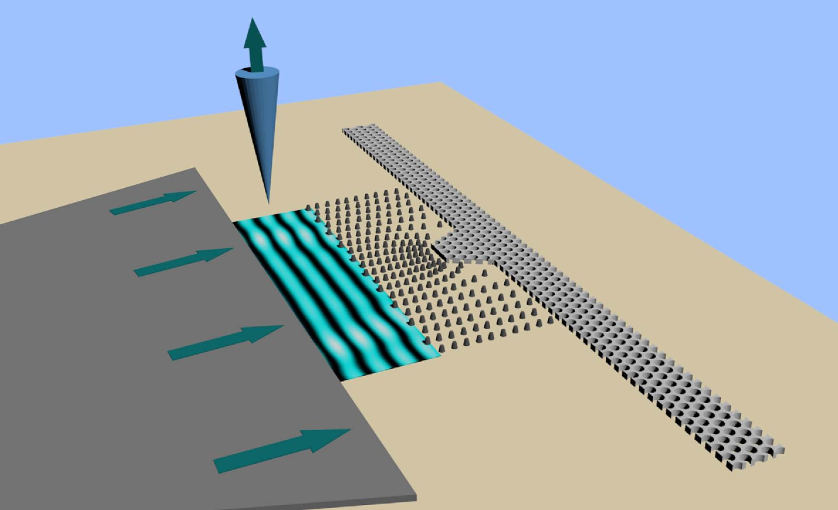
Herein, we propose to mimic the optical response of a flat mirror by a photonic crystal (PC) of irregular shape for wavelengths running in its band gap. This optical illusion is achieved using dielectric pillars with subwavelength diameter. The ability of reconstructing the wave fronts in the vicinity of the carpet is shown using near-field scanning optical microscopy (SNOM) Schonbrun et al. (2007). At optical frequencies, the previous TO-based carpet-cloaks were demonstrated by far-field microscopy methods Liu et al. (2008); Lee et al. (2009); Valentine et al. (2009) or leakage radiation microscopy Gabrielli et al. (2009). Those techniques are not suitable for our experimental setup described in Fig. 1. In this configuration, light successively propagates through free space and guiding areas over larges distances (more than 10 m between the very end of the injection guide and the input interface of the flat mirror). Thus, far-field microscopy would mainly allow access to scattered light such as out-of-plane losses, and leakage radiation microscopy would not be appropriate to measure wave fronts in the free space area. Such disadvantages clearly disappear with a near-field technique. SNOM provides a direct local probing of the electric field with a high spatial resolution thanks to the piezoelectric scanners associated with the probe. This markedly enhances our capabilities to manipulate light, even in the extreme near field limit, when a source lies in the close neighbourhood of the carpet-cloak Zolla et al. (2007).
The plan of the paper is as follows. We first describe a PC which is used to mimic a mirror and to realize the reference structure. A trapezoidal bump on one side of this PC plays the role of the object to hide. Next, a pillar structure designed using a quasi-conformal mapping is proposed to cloak the PC bump. Numerical simulations have been performed to show the efficiency of the design for wavelengths ranging from 1500 nm to 1650 nm. These composite strutures consisting of a combination of air holes and dielectric pillars have been fabricated with a novel one-mask process. Finally, near field measurements demonstrate the ability of the carpet to hide the bump in the near field at frequencies around the telecommunication wavelength 1550nm.
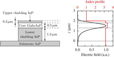
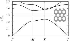
The first step is to consider a PC consisting of air holes in a dielectric matrix to build an efficient mirror at optical wavelengths. In view of the fabrication, the guiding structure defined in Fabre et al. (2008) is considered (see Fig. 2). It is made of a InGaAsP guiding layer with thickness and index 3.36, sandwiched between a 200-nm thick layer of InP with index 3.16 and a substrate made of the same material. For the sake of simplicity, this multilayer is modelled by an effective medium of index 3.26, corresponding to the effective index of the fundamental mode of this heterostructure (Fig. 2, right panel). As shown in Fig. 3, introduction of a hexagonal lattice of air holes of diameter nm and period nm into this homogeneous medium leads to the formation of a -polarization band gap for wavelengths ranging from 1280 nm to 1940 nm, i.e. for from to .
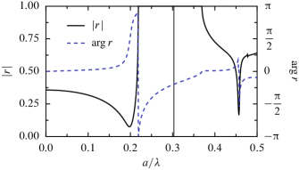
An additional challenge compared to a metallic mirror is the variation of the phase of the reflection coefficient within the band gap. Indeed, compared to ground carpet cloaks designed for curved metal surfaces, where the boundary condition is of the Dirichlet or Neumann type depending upon light’s polarization, a carpet cloak on a dielectric half-space Zhang et al. (2008) requires greater care, since the mathematical model now involves (anisotropic) transmission conditions at the interface between the carpet and the dielectric half-space (which in our case consists of a PC). In Fig. 4, the phase of reflection coefficient at normal incidence is shown to vary monotonically from to zero across the stop band. The resulting dispersion will have an adverse effect on broadband cloaking. More particularly, it is noted that, at the telecommunication wavelength corresponding to , the phase of the PC is much different from the phase shift of a mirror, which is only achieved at the lower edge of the stop band. This makes an unusual situation for the design of the carpet.
The goal of carpet-cloaking is to hide the bump of a trapezoidal shape as shown in Fig. 1 using an heterogeneous metamaterial (a medium with a subwavelength structure). In the present case, we opted for a carpet made of dielectric pillars. For this we build a quasi-grid deduced from conformal-optics considerations Li and Pendry (2008); Liu et al. (2008); Valentine et al. (2009); Gabrielli et al. (2009); Ergin et al. (2010); Renger et al. (2010): this approach preserves the isotropy of the medium, unlike conventional TO tools used for cloaking Pendry et al. (2006). We then place cylinders of diameter nm at the nodes of the transformed grid. We importantly note that the minimization of the modified Liao functional Liao and Liu (1993), which is usually invoked in recent papers on the carpet-cloaking, can be replaced by a potential computation. In other words, we build a conformal grid which preserves the right angles. If one can set up an electrostatic problem where the vertical lines are the electric field lines, then one can easily compute the equipotentials which are orthogonal at each point. The index distribution is then obtained numerically for each elementary cell of the grid using a simple vector product Li and Pendry (2008). The structure is then built by placing the dielectric pillars at the nodes of the conformal grid. We note that this approach has been successfully used for the design of a broadband plasmonic carpet Renger et al. (2010) and it is reminiscent of the work of Liang and Li Liang and Li (2011), where Bloch waves follow curved trajectories in transformed photonic crystals. The air holes in the PC and the dielectric pillars in the carpet have comparable diameters, hence the pillars are not deeply subwavelength in the stop band. Our PC carpet can therefore be considered as an intermediate configuration between a transformed PC (Bragg regime) and a conformal metamaterial (homogenization regime), keeping in mind artificial anisotropy is unwanted here.
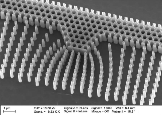
The device is fabricated using advanced nanoelectronics techniques on III–V semiconductors. We start from an InP–based heterostructure (InP–/InGaAsP–/InP–) grown by molecular beam epitaxy to confine light (at ) in the vertical direction. To create the two-dimensional patterning, we take benefit of the one-mask process primarily developed for photonic crystal based flat lenses Fabre et al. (2008). In brief, we employ a negative resist (HSQ) mask used for the electron beam lithography step to define simultaneously the matrix of the reflector, the pillars of the cloaking area as well as the injection guide constituted here of a monomode ridge waveguide progressively enlarged to form the quasi-plane wave requested to illuminate the device. After development and a densification by an O2 plasma of the HSQ resist, the mask is kept for the inductively coupled plasma (ICP) etching step. The fabricated device, shown in Fig. 5, confirms that the process is able to achieve in one step 200 nm diameter pillars even in close proximity (separation less than 50 nm in front of the reflector) and a PC with a period of 470 nm and 347 nm hole diameter over a depth larger than . The highly anisotropic character of the etching is preserved, which permits to reproduce with a high degree of accuracy the theoretical dimensions targeted.
The etching depth, larger than , plays a vital role. For our combined hole/pillar device, etching kinetics depends on the local environment due to species evacuation. Etching velocity is significantly lower in hole areas than in pillar regions. The process has been optimized to reach hole depths of about Fabre et al. (2006), leading to pillar heights between 2 and . Both values are sufficient to ensure that the integrated device works in a regime which can be accurately modelled by a two-dimensional system since most of the electromagnetic energy of the guided mode will be controlled by the etching, as demonstrated in Fig. 2. In addition, it can be expected from Fig. 2 that the out-of-plane losses are not significant and do not disturb the behavior of the carpet, an assumption which will be experimentally validated in the sequel. This large etching depth is a key point of our fabrication process which combines holes and pillars: This yields high quality results for the field measurements.
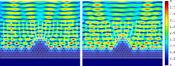
Indeed, in Fig. 6 the concept is verified using SNOM in collection mode Fabre et al. (2008). Thanks to the configuration of both devices and experimental set up, a phase imaging is performed by a unique near field intensity measure without optical heterodyne detection Schonbrun et al. (2007). The measurement of the reflection on a flat photonic crystal (upper panel) is similar to the lower panel (cloaked bump). We can see a significant improvement compared to the bump taken on its own in the middle panel. Before considering the optical images, it is important to note that the deep etching of the structures leads to large vertical displacements of the probe during the near-field scans, which may affect the formation of the optical images. However, despite this strongly modulated topology, the submicrometric features of the samples are properly resolved in all cases, which is particularly challenging on the sharp pillars of the cloak as well as on the photonic crystal mirrors. A three-dimensional view of the measured topography is provided for illustration purposes in Fig. 8a.
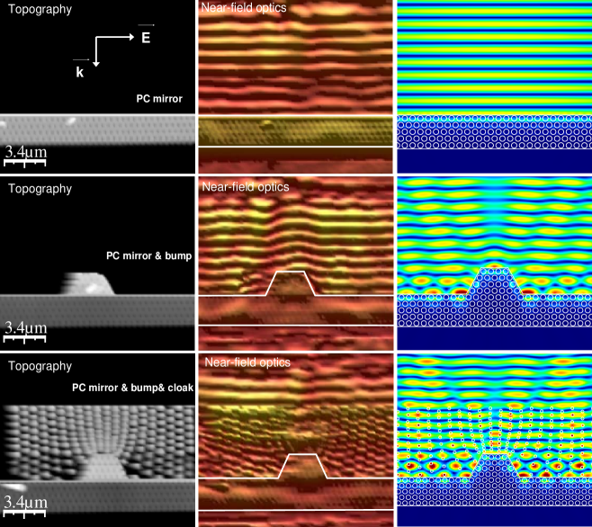
The optical images, shown in Fig. 6, present the typical optical behaviour of the different structures at a telecommunication wavelength of 1540 nm. A standard illuminated view of the optical images is chosen here for the images representation because of a lateral modulation of the intensity of the plane wave impinging on the structure. This can be attributed to a non-adiabatic tapering of the input waveguides. However, as shown hereafter, this is not an issue for the reported observations since it is the shape of the wave fronts that are required for interpretation and not their relative intensity.
On the optical images, one can observe the standing wave patterns between the incident and reflected wave by the photonic crystal mirror. In the case of the reference structure made of the PC flat mirror, flat interference fringes with a half-wavelength spatial periodicity are clearly resolved on the optical near-field images. Then, introducing a defect on the planarity of the PC mirror surface, namely a bump, leads to a local deformation of the planarity of the standing wave pattern. More precisely, as clearly visible on the near-field measurement, a half-period shift of the fringes is measured locally above the bump on the mirror, which corresponds to a local phase shift of the reflected wave. As a consequence, cloaking the bump would result in suppressing this phase shift on the observed interference pattern. Experimentally, the near-field images recorded on the cloak structures reveal almost flat fringes in front of the cloak, which testifies that the bump has been properly cloaked.
Since the contrast of these fringes remains the same as in the reference cases without cloak and since the reflectivity of the first row of the cloak pillars is low due to their subwavelength size, these flat fringes clearly result from the interference between the wave reflected by the photonic crystal mirror after passing through the cloak and the incident plane wave. Then, inside the cloak, as visible on all the presented images in Fig. 6 and 8, the measured optical near-field distributions are unfortunately highly modulated by the cloak topography (Fig. 8a), making us blind to the standing wave pattern inside it.
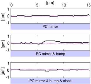
In addition, a quantitative measure of the cloaking efficiency can be derived from the evaluation of the modified Liao functional Liao and Liu (1993). The fringes are defined as the lines corresponding to the maxima of the field intensity. Figure 7 shows these fringes for the three situations. According to the method of least squares, it is found that the deviations from a segment are respectively 37, 129 and 52 for the flat mirror, the flat mirror with bump, and the cloaked structure (arbitrary unit is used). These raw data show that the measurements and the device’s imperfections induce uncertainties which make the error bars very wide. However, when restricting the evaluation of the deviation to the segment centred above the bump, the deviations become respectively 13, 76 and 16. In this case, it is found that the carpet leads to a reduction of the bump signature by a factor of 4.75, which is comparatively higher than the reduction factor of 3.7 obtained for a plasmonic carpet at 800 nm in Renger et al. (2010).
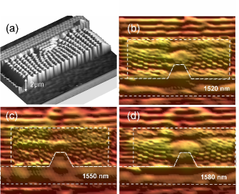
As shown in Fig. 8, such experimental features, the strongly topographically modulated light inside the cloak as well as the standing wave with flat fringes showing the cloak effect, are observed all over the C-band of telecommunication wavelengths, i.e. for wavelengths ranging from 1520 nm to 1580 nm. This wavelength range is limited experimentally at shorter wavelengths by the absorption of the InGaAs layer used for waveguiding and at longer wavelengths by our laser source. However, numerical simulations show that the carpet operates for a broad band of wavelengths ranging from to (see figure 9).
In conclusion, a new cloaking device with a photonic crystal mirror has been designed to operate at the telecommunication wavelength 1550 nm. This device has been fabricated using an original technique based on a novel one-mask process which makes it possible to create pillars and holes with an etching depth larger than . The characterisation of the cloaking structure has been performed with near-field measurements showing the interference fringes in the closeness of the cloaking structure. The invisibility carpet is shown to operate very efficiently for wavelengths ranging from 1520 nm to 1580 nm (and from nm to nm in theory): A reduction factor of 4.75 has been achieved for the bump signature. We note that our design should also work for visible wavelengths: To achieve this goal theoretically, one need only scale down the PC structure by a factor 2, as in this case, the stop band ranges from 670 nm to 1020 nm for a lattice constant of 235 nm and a diameter of air holes of 173.5 nm. The main difficulty lies in fact in downscaling the carpet cloak, as this would bring down the diameter of pillars to 100 nm, which remains a technological challenge for us: The pillars should be tall enough in order to ensure the two-dimensional nature of the problem.
Acknowledgements.
This work was partly supported by the project FANI funded by the Agence Nationale de la Recherche (ANR). S.G. acknowledges funding from the European Union through ERC Starting Grant Anamorphism. G.S. would like to thank the Regional Council of Burgundy for financial support. Dr. Jensen Li is gratefully acknowledged for useful discussions.References
- Pendry et al. (2006) J. B. Pendry, D. Schurig, and D. R. Smith, Science 312, 1780 (2006)
- Leonhardt (2006) U. Leonhardt, Science 312, 1777 (2006)
- Schurig et al. (2006) D. Schurig, J. J. Mock, B. J. Justice, C. A. Cummer, J. B. Pendry, A. F. Starr, and D. R. Smith, Science 314, 977 (2006)
- Kanté et al. (2009) B. Kanté, D. Germain, , and A. de Lustrac, Phys. Rev. B 80, 201104 (2009)
- Greenleaf et al. (2003) A. Greenleaf, A. Lassas, and G. Uhlmann, Math. Res. Lett. 10, 685 (2003)
- Leonhardt and Tyc (2009) U. Leonhardt and T. Tyc, Science 323, 110 (2009)
- Percze et al. (2011) J. Percze, T. Tyc, and U. Leonhardt, New Journal of Physics 13, 083007 (2011)
- Kohn et al. (2011) R. V. Kohn, H. Shen, M. S. Vogelius, and M. I. Weinstein, Inverse Problems 24, 015016 (2011)
- Jiang et al. (2008) W. X. Jiang, T. J. Cui, X. M. Yang, Q. Cheng, R. Liu, and D. R. Smith, Appl. Phys. Lett. 92, 264101 (2008)
- Li and Pendry (2008) J. Li and J. B. Pendry, Phys. Rev. Lett. 101, 203901 (2008)
- Cho (2010) A. Cho, Science 329, 277 (2010)
- Liu et al. (2008) R. Liu, C. Ji, J. J. Mock, J. Chin, T. J. Cui, and D. R. Smith, Science 323, 366 (2008)
- Lee et al. (2009) J. H. Lee, J. Blair, V. A. Tamma, Q. Wu, S. J. Rhee, C. J. Summers, and W. Park, Optics Express 17, 12922 (2009)
- Valentine et al. (2009) J. Valentine, J. Li, T. Zentgraf, G. Bartal, and X. Zhang, Nature Mater. 8, 569 (2009)
- Gabrielli et al. (2009) L. H. Gabrielli, J. Cardenas, C. B. Poitras, and M. Lipson, Nat. Photonics 8, 461 (2009)
- Ergin et al. (2010) N. Ergin, T. andStenger, P. Brenner, J. B. Pendry, and M. Wegener, Science 328, 337 (2010)
- Renger et al. (2010) J. Renger, M. Kadic, G. Dupont, S. S. Aćimović, S. Guenneau, R. Quidant, and S. Enoch, Opt. Express 18, 15757 (2010)
- Chen et al. (2011) X. Chen, Y. Luo, J. Zhang, K. Jiang, J. B. Pendry, and S. Zhang, Nature Com. 2, 176 (2011)
- Schonbrun et al. (2007) E. Schonbrun, Q. Wu, W. Park, T. Yamashita, C. J. Summers, M. Abashin, and Y. Fainman, Appl. Phys. Lett. 90, 041113 (2007)
- Zolla et al. (2007) F. Zolla, S. Guenneau, A. Nicolet, and J. B. Pendry, Opt. Lett. 32, 1069 (2007)
- Fabre et al. (2008) N. Fabre, L. Lalouat, B. Cluzel, X. Mélique, D. Lippens, F. de Fornel, and O. Vanbésien, Phys. Rev. Lett. 101, 073901 (2008)
- Zhang et al. (2008) P. Zhang, Y. Jin, and S. He, Opt. Express 16, 3161 (2008)
- Liao and Liu (1993) G. Liao and H. Liu, Num. Math. PDEs 9 (1993)
- Liang and Li (2011) Z. Liang and J. Li, Opt. Express 19 (2011)
- Fabre et al. (2006) N. Fabre, S. Fasquel, C. Legrand, X. Mélique, M. Muller, M. François, O. Vanbésien, and D. Lippens, Opto-Electron. Rev. 14, 225 (2006)