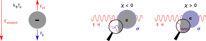
Surface electrons at plasma walls
Abstract
In this chapter we introduce a microscopic modelling of the surplus electrons on the plasma wall which complements the classical description of the plasma sheath. First we introduce a model for the electron surface layer to study the quasistationary electron distribution and the potential at an unbiased plasma wall. Then we calculate sticking coefficients and desorption times for electron trapping in the image states. Finally we study how surplus electrons affect light scattering and how charge signatures offer the possibility of a novel charge measurement for dust grains.
1 Introduction
When a macroscopic object is brought into contact with an ionised gas its surface is exposed to a fast influx of electrons. Due to the collection of electrons it acquires a negative charge. The wall electrons give rise to a repulsive Coulomb potential which reduces the further influx of electrons until—in quasi-stationarity—electron and ion flux onto the surface balance each other. This coincides with the formation of the plasma sheath, an electron depleted region adjacent to the wall.
The traditional modelling of the plasma wall focuses mainly on the plasma sheath which is a macroscopic manifestation of the charge transfer at the plasma boundary. Electrons and ions are usually assumed to annihilate instantly at the wall. Thus the wall is considered to be a perfect absorber for the charged species of the plasma. This boundary condition implicitly assumes that the charge transfer at the plasma wall occurs on time and length scales too short to be of significance for the development of the discharge. It is thus not necessary to track them Franklin76 . Improvements to the perfect absorber condition characterise the wall by an electron-ion recombination coefficient and secondary electron emission coefficients for various impacting species. Still, replacing the electron kinetics by an ad-hoc boundary condition does not allow for a description of the charge transfer at the surface.

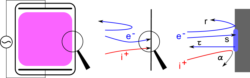
While this approach may be sufficient for large discharges with small surface to volume ratios it becomes questionable for the modelling of small discharges with large surface to volume ratios. Indeed, the nature and build-up of surface charges have received increasing attention in various novel set-ups of bounded plasmas (illustrated in Fig. 1). In dusty plasmas BBB09 ; PAB08 ; FIK05 , for instance, the charge soaked up by the dust particles controls the overall charge balance of the discharge BKS06 . Moreover, the particle charge controls the interaction between dust particles and between dust particles and external electromagnetic fields. The particle charge is thus a central quantity of interest which should be known as precisely as possible. In dielectric barrier discharges GMB02 ; WYB05 ; BMG05 ; SLP07 ; BWS12 ; BNW12 or microplasmas BSE06 ; Kushner05 surface charges determine the spatio-temporal structure of the discharge Kogelschatz03 . Surface charges, for instance, may pin the filaments in the filamentary mode of the dielectric barrier discharge and give the discharge a memory across several cycles. Lastly, in solid-state based microdischarges THW11 ; DOL10 , the miniaturisation of the discharge increases the surface to volume ratio to such an extent that the (biased) plasma wall becomes an integral part of the discharge. The charge transfer from the plasma into the solid and vice versa may even be used explicitly, as for instance in the plasma transistor WTE10 .
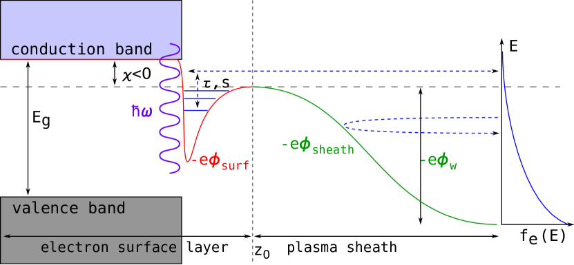
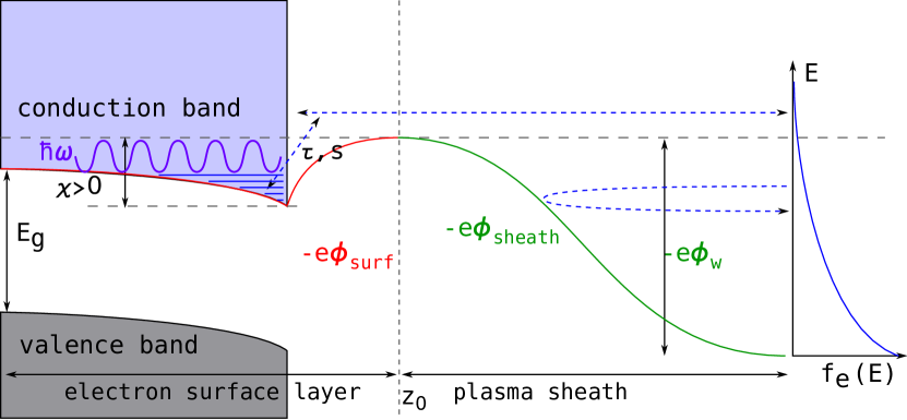
While the most prominent effect of charge transfer at the plasma wall is the plasma sheath the microscopic processes responsible for it cannot be captured in any sheath model which is solely based on the long range Coulomb potential and classical mechanics. Inspired by Emeleus and Coulter EC87 as well as Behnke and coworkers BBD97 ; GMB02 who envisaged a surface plasma of ions and electrons coupled to the bulk plasma by phenomenological rate equations characterised by sticking coefficients, residence times, and recombination coefficients we consider the build-up, distribution and release of surface electrons from a surface physics perspective. A sketch of the wall bound-processes which cannot be described in a sheath model is given by Fig. 2. The description of the plasma boundary has thus to be augmented by an interface region—the electron surface layer (ESL)—which encompasses not only the Coulomb potential but also short ranged surface potentials. This gives a framework for identifying electron trapping sites, determining the electron distribution and the potential across the interface in quasi-stationarity and calculating electron sticking coefficients. Moreover it serves us to discuss the optical properties of the electron adsorbate on a dust grain.
In the following section we will introduce our model for the ESL for an unbiased plasma wall. In section 3 we will calculate sticking coefficients and desorption times, that are average residence times at the surface, for the case where electron trapping takes place in the image states in front of the surface. Finally in section 4 we apply our microscopic model to the electrons on a dust particle in order to study charge signatures in light scattering by a spherical dust particle and propose thereby a novel optical charge measurement.
2 Electron surface layer
After the initial charge-up is completed the plasma wall carries a negative charge. In this section we extend the modelling of the plasma boundary to the region inside the solid and calculate the plasma-induced modifications of the potential and charge distribution of the surface within a quasi-static model. Although knowing the potential and charge distribution across the interface may not be of particular importance for present day technological plasmas, it is of fundamental interest from an interface physics point of view. In addition, considering the plasma wall as an integral part of the plasma sheath may become critical when the miniaturisation of solid-state-based plasma devices continues.
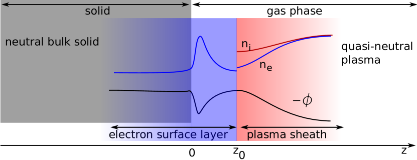
The current modelling of the plasma wall focuses on the plasma sheath and gives the potential as well as the electron and ion densities across that region. Our model for the ESL extends this into the solid HBF12 . Specifically, we calculate the potential as well as the distribution of wall bound electrons. Moreover, we give the spatial position, width and chemical potential of the surplus electrons. For this we use a graded interface potential Stern78 to interpolate between the sheath and the wall potential and distribute the surplus electrons making up the wall charge in this potential under the assumption that at quasi-stationarity they are thermalised with the wall TD85 .
As depicted in Fig. 3, we consider an ideal, planar interface at with the dielectric occupying the half-space and the discharge occupying the half-space . At the moment we focus on the physical principles controlling the electronic properties of the plasma-wall interface. Chemical contamination and structural damage due to the burning gas discharge are discarded. In the model we propose the wall charge to be treated as an ESL, which is an interface specific electron distribution thermalised with the solid stretching from the plasma sheath over the crystallographic interface into the bulk of the dielectric.
The boundary between the ESL and the plasma sheath at is located in front of the surface. It is the position where the attractive force due to the surface potential and the repulsive force due to the sheath potential balance each other. Thus, is given by
| (1) |
For an electron is attracted to the surface and thus contained in the ESL while for it is repelled back into the plasma. The position is an effective wall for plasma electrons and ions at which the flux balance between electron flux and ion flux has to be fulfilled. In the following we use for simplicity the perfect absorber model . The effective wall position also gives the distance to the surface at which the description of the plasma sheath based on the long-range potential breaks down as the short-range surface potential becomes dominant. On the solid side, for , the ESL is bounded because of the shallow potential well formed by the restoring force from the positive charge in the plasma sheath.
Within this quasi-static model the electrons missing in the sheath are accumulated on the surface. For the construction of our one-dimensional interface model we need the total number per unit area of missing sheath electrons (that is, the total surface density of missing sheath electrons) as a function of the wall potential because it is this number of electrons which can be distributed across the ESL. Hence, we require a model for the plasma sheath.
For simplicity, we use a collision-less sheath model Franklin76 , more realistic sheath models Franklin76 ; LL05 ; Riemann91 make no difference in principle. In the collision-less sheath electrons are thermalised, that is, the electron density , with the potential, the plasma density and the electron temperature. The ions enter the sheath with a directed velocity and satisfy a source-free continuity equation, , implying , and an equation of motion , with the ion density, and the ion mass. The potential satisfies Poisson’s equation . Thus, the governing equations for the collision-less plasma sheath are Franklin76
| (2) |
and
| (3) |
Introducing dimensionless variables , and , where and , equations (2) and (3) become
| (4) |
In the ESL model the plasma occupies not the whole half space but only the portion (see Fig. 3). Integrating the first equation gives , where is the reduced velocity of ions entering the sheath, so that the second equation becomes
| (5) |
Using the boundary condition that the potential and the field vanish far inside the plasma, that is, and for , Eq. (5) can be integrated once and we obtain
| (6) |
For ions entering the sheath with the Bohm velocity . The field at the effective wall as a function of the wall potential is then given by
| (7) |
The total surface density of ions in the sheath equals the total surface density of electrons in the ESL . It can be related by Poisson’s equation to the field at the wall and reads
| (8) |
Combing Eqs. (8) and (7) gives the total surface density of electrons to be inserted into the ESL as a function of the wall potential.
The wall potential itself is determined by the flux balance condition, , which, in the ESL model, is assumed to be fulfilled at . Using the Bohm flux for the ions and the thermal flux for the electrons,
| (9) |
the wall potential is given by Franklin76
| (10) |
that is,
| (11) |
In the collision-less sheath model the wall potential depends only on the electron temperature and the ion to electron mass ratio.
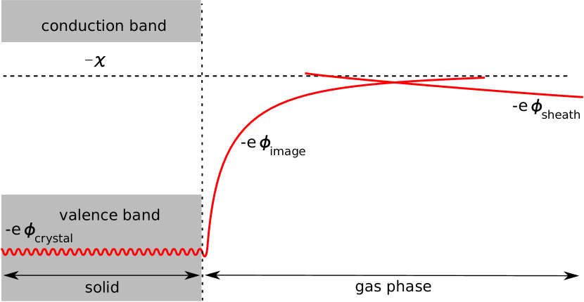
We can now move on to the distribution of surplus electrons in the surface layer. It is primarily determined by the potential in the interface region surrounding an ideal dielectric interface. We first single out the relevant microscopic potentials at the interface (illustrated in Fig. 4) and then describe an effective model for them (Fig. 5).
Far away from the surface the potential is given by the repulsive sheath potential. Closer to the surface an attractive surface potential, the image potential, which stems from the dielectric mismatch at the interface, becomes dominant. Classically the image potential is given by the expression Jackson98
| (12) |
where is the static dielectric constant. This expression is valid far away from the wall. Closer to the wall the shape is modified as the potential merges continuously with the crystal potential in the bulk of the dielectric. Even more important inside the dielectric is the band structure. For a dielectric the valence band is full while the conduction band is completely empty. Thus surplus electrons can populate the conduction band and the conduction band minimum acts as a long range potential for the electrons. In addition to the image potential, the surface potential comprises an offset due to a charge double layer formed immediately at the surface. It is due to electron density leaking out of the solid as a consequence of free energy minimisation or to relaxation and polarisation of the atomic bonds at the surface as a consequence of the truncation of the lattice. This offset of the conduction band minimum at the surface to the potential in front of it is characterised by the electron affinity of the solid . For the conduction band minimum lies above the potential just in front of the solid, for it lies below it. So far we have considered an uncharged surface. This raises the question whether the electronic structure of the surface is changed by the surplus electrons from the plasma. In comparison to the electrons responsible for the chemical binding within the dielectric the additional electrons coming from the plasma are only a few. The available electronic states and the offset of the energy bands in the bulk with respect to the potential outside the dielectric will thus not be changed significantly by the presence of the wall charge. Note however that a chemical modification of the plasma wall can change the electronic structure. In particular the electron affinity is susceptible to surface coating and adatoms. Surface termination by elements with small electronegativity, for instance hydrogen, may induce a negative electron affinity CRL98 while elements with larger electronegativity, for instance oxygen, can lead to a positive electron affinity MRL01 .
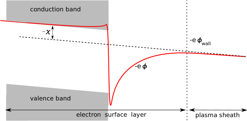
From these microscopic potentials we construct an effective surface potential. To obtain a realistic image and offset potential without performing an atomistically accurate calculation we employ the model of a graded interface. This model is parametrised by experimentally measured (or where not available theoretically calculated) values for the electron affinity, the dielectric constant, and the conduction band effective mass. First proposed by Stern Stern78 to remove the unphysical singularity of the image potential at and later extended to potential offsets at semiconductor heterojunctions SS84 it assumes the smooth variation of parameters that change abruptly at the interface over a length on the order of the lattice constant. For our purposes we assume a sinusoidal interpolation of the dielectric constant, offset of the long range potential and effective electron mass with a grading half-width of HBF12 . The model does not account for effects associated with intrinsic surface states (Shockley or Tamm states Lueth ) or additional states which may arise from the short-range surface potential. Nevertheless the graded interface model is a reasonable description of the surface, suited for dielectrics with ionic bonds which typically have no intrinsic surface states.
The total surface potential
| (13) |
comprises the graded image and offset potential. It is continuous across the crystallographic interface at and enables us thereby to also calculate a smoothly varying electron distribution in the ESL.
Using Eq. (1) we can now determine the position of the effective wall, that is, the maximum extent of the ESL on the plasma side. The derivative of the surface potential is . Due to the relatively weak field in the sheath compared to the image force, the boundary will be so far away from the interface that vanishes and the image potential obeys (12). Thus, the boundary between the ESL and the plasma sheath is given by
| (14) |
with , and given by (7).
We can now turn to the distribution of the plasma-supplied excess electrons in the ESL. For this quasi-static model we assume that the wall-bound surplus electrons are in thermal equilibrium with the wall. Thus, their distribution minimises the grand canonical potential and satisfies Poisson’s equation. Inspired by Tkharev and Danilyuk TD85 we apply density functional theory KS65 ; Mermin65 to the graded interface. For the purpose of this exploratory calculation we will use density functional theory in the local approximation. Quite generally, the grand canonical potential of an electron system in an external potential is given in the local approximation by
| (15) |
where is the grand canonical potential of the homogeneous system with density and the Coulomb potential is determined by
| (16) |
The ground state electron density minimises , that is, it satisfies
| (17) |
where is the chemical potential for the homogeneous system.
In our one-dimensional graded interface model Eq. (17) reduces to
| (18) |
where , and the electrostatic potential
| (19) |
consists of the potential of the bare surface given by Eq. (13) and the internal Coulomb potential which satisfies Poisson’s equation
| (20) |
with the graded dielectric constant . The boundary conditions and guarantee continuity of the potential at and include the restoring force from the positive charge in the sheath. Note that the Coulomb potential derived from this equation already includes the attraction of an electron to the image of the charge distribution. The image potential contains only the self-interaction of an electron to its own image.
For the functional relation we take the expression adequate for a homogeneous, non-interacting, non-degenerate electron gas
| (21) |
where is the graded effective electron mass. This is justified because the density of the excess electrons is rather low and the temperature of the surface is rather high, typically a few hundred Kelvins.
For the calculation of the quasi-stationary distribution of surplus electrons Eqs. (18) and (20) have to be solved iteratively (until is stationary) subject to the additional constraint which guarantees charge neutrality between the ESL and the plasma sheath. The position is a cut-off which has to be chosen large enough in order not to affect the numerical results. In a more refined model for the ESL the crossover of the wall charge to the neutral bulk of the dielectric can be taken into account by splitting the ESL into an interface specific region and a space charge region. This approach which turns from an ad-hoc cutt-off into the boundary between the two regions is described in HBF12 . For the charge distribution at the interface the simple model is however sufficient.
We now use the ESL model to calculate for a helium discharge in contact with a LiF and Al2O3 surface the electron density and potential across the plasma wall. Our main focus lies in the identification of generic types of electron distributions in the ESL.

Depending on the electron affinity , one of two scenarios for the distribution of surplus electrons in the ESL may be realised. For negative electron affintiy , the conduction band minimum lies above the long-range potential just in front of the surface. It is thus energetically unfavourable for surplus electrons to populate the conduction band. Instead they are located in the image potential in front of the surface. The energy of an electron in the image potential reaches its minimum just in front of the surface at the beginning of the graded interface. This is confirmed by the electron density and the potential for LiF () shown in the left panel of Fig. 6. For , the excess electrons coming from the plasma form therefore an external surface charge in the image potential in front of the crystallographic interface. As the electrons do not penetrate into the solid the band bending associated with it is negligible. The external surface charge is very narrow. It can thus be considered as a quasi-two-dimensional electron gas, similar to the surface plasma anticipated by Emeleus and Coulter EC87 ; EC88 .
For positive electron affinity the situation is dramatically different. In this case the conduction band minimum is below the potential just outside. It is thus energetically favourable for electrons to accumulate inside the dielectric. This can be seen in the right panel of Fig. 6 which shows the electron density and the potential for an Al2O3 surface (). Although the image potential still induces an attractive well in front of the surface the minimum of the potential energy for electrons is reached inside the dielectric. Excess electrons coming from the plasma are thus mostly located inside the wall where they form a space charge in the conduction band. The electron distribution extends deep into the bulk and entails bending of the energy bands near the surface. Note the different scales of the axes for the left and right panels of Fig. 6. On the scale where variations in the space charge for Al2O3 are noticeable the electron distribution for LiF is basically a vertical line.
So far we have shown the potential and the electron distribution in the ESL. Now, we will compare the potential and the charge distribution in the ESL with the ones in the plasma sheath. The wall bound electrons in the surface layer constitute an electron distribution in thermal equilibrium with the wall which balances electron and ion influx at the sheath-ELS boundary . On top of this quasistationary electron distribution there are fluxes of electrons and ions, coming from the plasma. These currents, which begin at and persist to the location in the ESL where either electron trapping or electron-ion recombination takes place are not described by our simple ESL model. The electron and ion densities in this model are thus discontinuous at . The potential, however, which has been obtained from the integration of Poisson’s equation is continuous and differentiable everywhere. Between the crystallographic interface and the electron and ion flux from the plasma would be important. The neglect of the charge densities associated with these fluxes does however not affect the potential because they are too small to have a significant effect.
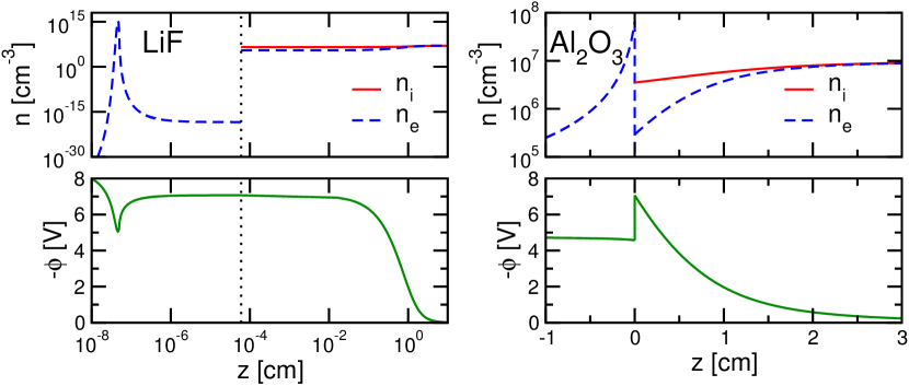
Figure 7 compares the ESL and the plasma sheath for LiF (, left) and Al2O3 (, right). We plot the electron and ion densities (upper panel) as well as the electric potential (lower panel). Note the logarithmic scale in the left panel and the linear scale in the right panel. For LiF the surface electrons are bound in the image states in front of the surface due to the negative electron affinity. Far from the surface, the potential approaches the bulk plasma value chosen to be zero. In the sheath the potential develops a Coulomb barrier and reaches the wall potential at , the distance where the sheath merges with the surface layer (vertical dotted line). The wall potential is the potential just outside to which the energies of the bulk states are referenced. Closer to the surface the potential follows the attractive image potential while at the surface the repulsive potential due to the negative electron affinity prevents the electron from entering the dielectric (only scarcely seen on the scale of the figure).
For Al2O3 the excess electrons constituting the wall charge penetrate deep into the dielectric due to the positive electron affinity. Compared to the variation of the electric potential in the sheath the band bending in the dielectric induced by the wall charge is rather small as indicated by the variation of inside the dielectric. This is because is large and most surplus electrons are bound close to the crystallographic interface. The interface specific region where the short ranged surface potential varies strongly is very narrow compared to the extent of the two space charge regions.
The ESL should be regarded as the ultimate boundary layer of a bounded gas discharge. Our model for the ESL captures the coupling of the neutral bulk plasma to an electron plasma at the boundary separated from the bulk plasma by the plasma sheath. Depending on the electron affinity this boundary plasma can be either a quasi-two-dimensional electron plasma or an electron(-hole) plasma inside the wall.
3 Electron physisorption
We can now turn to the electron kinetics in the ESL. Depending on the electron affinity two distinct scenarios for electron trapping emerge which are schematically shown in Figs. 8 and 9. For negative electron affinity (see Fig. 8) electrons that overcome the sheath potential do not penetrate the solid as their energy falls in the band gap where no internal states are available. Instead, they are trapped in the image potential in front of the surface. Energy-relaxation is in this case due to surface vibrations which trigger transitions to the bound image states. As the image potential is relatively deep compared to the energies of the longitudinal acoustic phonon responsible for electron trapping and the wavefunctions of the unbound states are suppressed close to the surface the probability for sticking is small. This scenario, which we have investigated in detail HBF10a ; HBF10b ; HBF11 , will be presented below.
For positive electron affinity (see Fig. 9) electrons that overcome the sheath potential penetrate into the solid. There they initially occupy high-lying states of the conduction band. Subsequent electron energy relaxation is due to scattering with bulk phonons of the dielectric and the plasma-supplied electrons are eventually trapped at the bottom of the conduction band in the potential well created by the restoring force from the plasma. Due to the high-density of states and an efficient scattering mechanism we expect the sticking coefficient to be much larger in this case. However, a detailed analysis of this scenario still remains to be done.
We will now consider the physisorption of an electron in the image potential in front of a dielectric with in detail. We describe the time evolution of the occupancy of the bound surface states with a quantum-kinetic rate equation GKT80a ; KG86 . It captures all three characteristic stages of physisorption: initial trapping, subsequent relaxation and desorption IN76 ; Brenig82 .
The time dependence of the occupancies of the bound states is given by GKT80a ; KG86
| (22) |
which can be rewritten as
| (23) |
where is the probability per unit time for a transition from a bound state to another bound state , and are the probabilities per unit time for a transition from the bound state to the continuum state and vice versa, and is the transit time through the surface potential of width , which, in the limit , can be absorbed into the transition probability. The matrix is defined implicitly by the above equation. The last term in Eqs. (22) and (23), respectively, gives the increase in the bound state occupancy due to the coupling between bound and unbound surface states.
The probability for an approaching electron in the continuum state to make a transition to any of the bound states is given by the prompt energy-resolved sticking coefficient
| (24) |
Treating the incident electron flux as an externally specified parameter, the solution of Eq. (22) describes the subsequent relaxation and desorption. It is given by
| (25) |
where and are the right and left eigenvectors to the eigenvalue of the matrix .
If the modulus of one eigenvalue, , is considerably smaller than the moduli of the other eigenvalues, , a unique desorption time and a unique sticking coefficient can be identified KG86 . In this case governs the long time behaviour of the equilibrium occupation of the bound states, , and its inverse can be identified with the desorption time, . The bound state occupancy splits into a slowly varying part given by the summand in Eq. (25) and a quickly varying part given by the sum over in Eq. (25).
The electron adsorbate, i.e. the fraction of the trapped electron remaining in the surface states for times on the order of the desorption time, is given by the slowly varying part only, . Differentiating with respect to the time,
| (26) |
we can, following Brenig Brenig82 , identify the kinetic energy-resolved sticking coefficient
| (27) |
giving the probability for both, initial trapping and subsequent relaxation.
If the incident unit electron flux corresponds to an electron with Boltzmann distributed kinetic energies, the prompt or kinetic energy-averaged sticking coefficient is given by
| (28) |
where is the mean electron energy.
[width=0.5]figure10
These kinetic equations rely on the knowledge of the transition probabilities. They have to be calculated from a microscopic model for the electron-surface interaction. The image potential supports a series of bound states which can trap electrons temporarily at the surface. Transitions between image states are due to dynamic perturbations of the surface potential. The image potential is very steep near the surface. A particularly strong perturbation arises therefore from the surface vibrations induced by the longitudinal acoustic bulk phonon perpendicular to the surface. Describing them with a Debye model, the maximum phonon energy of this mode is the Debye energy . Measuring energies in units of the Debye energy, important dimensionless parameters characterising the potential depth are
| (29) |
where is the energy of the bound state.
The depth of the image potential can be classified with respect to the Debye energy. If , we call the potential -phonon deep. If we call it shallow. For a shallow potential the lowest bound state is coupled by a one-phonon transition to the continuum. If the potential is -phonon deep an -phonon process links the lowest bound state to the second bound states, which is linked by one-phonon transitions either directly or via intermediates to the continuum. For the dielectrics which we consider the potential is two-phonon (MgO) or three-phonon deep (LiF). A schematic representation of the image states is given in Fig. 10.
For the calculation of the transition probabilities used in the rate equation we need a microscopic model for the image potential and the electron-surface vibration interaction. Classically the image potential ensues from the dielectric mismatch at the interface. On a microscopic level it arises from the coupling of the electron to a polarisable surface mode of the solid. For a dielectric this is a surface phonon. For LiF and MgO the low frequency dielectric function is dominated by a transverse optical (TO) phonon with frequency . It can be approximated by EM73
| (30) |
where is the static dielectric constant. The bulk TO-phonon gives rise to a surface phonon. Its frequency is determined by the condition . The electron couples to this surface phonon according to EM73 ; Barton81
| (31) |
with
| (32) |
where and the subscript denotes vectors parallel to the surface and are annihilation (creation) operators for surface phonons.
Applying a unitary transformation Barton81 separates the coupling into a static part which takes the classical form of the image potential and a dynamic part of the electron-surface phonon coupling, which encodes recoil effects and encompasses momentum relaxation parallel to the surface. While the classical image potential allows a simple description of the image states which captures their properties fairly well it is not sufficient for the calculation of probabilities for surface vibration induced transitions, as they perturb the electronic states most strongly close to the surface where the image potential is steepest. Unfortunately, in this region the classical image potential has an unphysical divergence. To remedy this we use a variational procedure to extract the static image potential from EM73 . Thereby we keep some recoil effects which make the recoil-corrected image potential with a cut-off parameter HBF10a divergence free.
Transitions between the eigenstates of the recoil-corrected image potential are due to the longitudinal-acoustic bulk phonon perpendicular to the surface. The Hamiltonian from which we calculate the transition probabilities is given by
| (33) |
where
| (34) |
describes the electron in the recoil-corrected image potential,
| (35) |
describes the free dynamics of the bulk longitudinal acoustic phonon responsible for transitions between surface states, and
| (36) |
denotes the dynamic coupling of the electron to the bulk phonon.
The perturbation can be identified as the difference between the displaced surface potential and the static surface potential. It reads, after the transformation ,
| (37) |
In general, multi-phonon processes can arise both from the nonlinearity of the electron-phonon coupling as well as from the successive actions of encoded in the T matrix equation,
| (38) |
where is given by
| (39) |
The transition probability per unit time from an electronic state to an electronic state encompassing both types of processes is given by BY73
where , with the surface temperature and and the initial and final phonon states. We are only interested in the transitions between electronic states. It is thus natural to average in Eq. (3) over all phonon states. The delta function guarantees energy conservation.
In principle, multiphonon transition rates can be obtained by iterating the T-matrix and evaluating Eq. (3). Up to , for instance, the T-matrix reads
| (40) |
where the originate from expanding Eq. (37) in the displacement . The T-matrix enters as into the transition probability. The term can be identified as the Golden Rule transition probability. Proportional to it is a one-phonon process. Two-phonon processes, proportional to , are represented by the terms
| (41) |
and
| (42) |
A complete two-phonon calculation would take all these processes into account as they stand. This is however not always necessary. A closer analysis (see HBF10a ) of the first group of terms reveals that they are two-phonon corrections to transitions already enabled by a one-phonon process. We assume that theses corrections are small and evaluate only the second group for transitions where they enable two-phonon transitions which are not merely corrections to one-phonon transitions. The details of the evaluation of the transition probabilities, including a regularisation of divergences by taking a finite phonon lifetime into account, can be found in HBF10a ; HBF10b .
The expansion of the T-matrix allows the calculation of transition probabilities for the two-phonon deep potentials of graphite and MgO. However, for a three-phonon deep potential, for instance for LiF and CaO, this approach is no longer feasible. From Refs. HBF10a ; HBF10b we qualitatively know the relevance of different types of multi-phonon processes. For continuum to bound state transitions, for instance, one phonon processes are sufficient at low electron energies. We will therefore compute the transition probabilities between bound and continuum states in the one-phonon approximation. For transitions between bound states, we found that multi-phonon processes due to the nonlinearity of the electron-phonon coupling tend to be more important than the multi-phonon processes due to the iteration of the T-matrix. Hence we expect that an approximation which takes only the nonlinearity of the electron-phonon interaction nonperturbatively into account to be sufficient for the identification of the generic behaviour of multi-phonon-mediated adsorption and desorption. This approach is described in HBF11 .
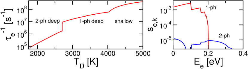
We now turn to results for the desorption time and the sticking coefficient for physisorption in the image states. Before showing results for MgO and LiF, we consider the dependence of the electron kinetics on the potential depth and the relevance of one or two-phonon processes. For this we show in the left panel of Fig. 11 the inverse of the desorption time as a function of the Debye temperature which sets the energy scale of the acoustic phonons. While the absolute depth of the potential remains constant, varying the phonon energy tunes the effective potential depth. Fig. 11 reveals that for a shallow potential desorption is most efficient while for a one-phonon deep potential it gradually becomes less efficient. When the potential becomes two-phonon deep desorption suddenly becomes even slower which reflects the small magnitude of two-phonon transitions compared to one-phonon transitions. This justifies our approximation of neglecting two-phonon corrections to transitions already enabled by a one-phonon process. For a Debye temperature the results apply to graphite.
[width=0.6]figure12
The energy-resolved prompt sticking coefficient, plotted in the right panel of Fig. 11 for graphite, shows that also for bound state-continuum transitions one-phonon processes far outweigh two-phonon processes. Thus, sticking is mainly due to one-phonon processes. Moreover we find that the sticking coefficient drops sharply at specific energies. These accessibility thresholds occur whenever one bound state becomes no longer accessible from the continuum because the energy difference exceeds one Debye energy.
The sticking coefficient takes relatively small values—on the order of . This is due to the small matrix elements between bound and continuum states. Fig. 12 shows the wave functions of representative bound and continuum states for MgO. For large energy the continuum wave functions have sinusoidal shape whereas for small energies their amplitude is significantly suppressed close to the surface. These two behaviours correspond to two limits for the wavefunction. For simplicity we discuss this for a potential without cut-off. The continuum wavefunctions read where . For we obtain which also holds for large while for we obtain . The proportionality to entails a strong suppression of the wavefunction for low energy.
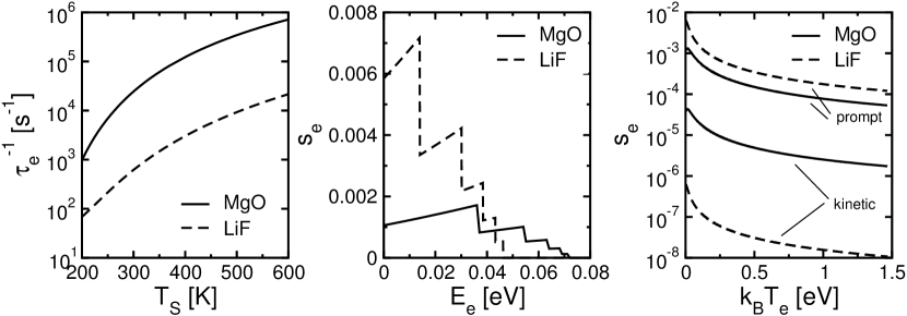
Electron physisorption at a dielectric surface with negative electron affinity is an intriguing phenomenon due to the interplay of potential depth, magnitude of matrix elements and surface temperature HBF10a ; HBF10b ; HBF11 . Initial trapping of the electrons, characterised by the prompt sticking coefficient, occurs in the upper bound states by one-phonon transitions. Relaxation after initial trapping depends on the strength of transitions from the upper bound states to the lowest bound states. If the lowest bound state was linked to the second bound state by a one-phonon process the electron would relax for all surface temperatures. If they are linked by a multiphonon process relaxation takes place only for low temperature, whereas for room temperature a relaxation bottleneck ensues as the electron desorbs from the upper bound states before it drops to the lowest bound state. This leads to a severe reduction of the kinetic sticking coefficient compared to the prompt sticking coefficient. The dominant desorption channel depends also on the depth of the potential. For a shallow potential desorption occurs directly from the lowest bound state to the continuum. For deeper potentials desorption proceeds via the upper bound states. Desorption occurs then via a cascade in systems without and as a one-way process in systems with relaxation bottleneck HBF11 . An overview of results for the desorption time as well as prompt and kinetic sticking coefficients for MgO and LiF is given by Fig. 13. Most important for the plasma context is that and HBF10a ; HBF10b ; HBF11 , implying that a dielectric surface with a negative electron affinity is not a perfect absorber for electrons.
4 Mie scattering by a charged particle
In the previous section we have employed our model for the ESL to analyse the electron kinetics at the plasma boundary and to calculate desorption times and sticking coefficients for a dielectric with negative electron affinity. Another application of the model for the ESL is the study of the optical properties of the wall-bound electrons. In this section we will study the effect of surplus electrons on the scattering of light by a sphere (Mie scattering) with an eye on a charge measurement for dust particles. Most established methods for measuring the particle charge CJG11 ; KRZ05 ; TLA00 require plasma parameters which are not precisely known. The particle charge, however, is the fundamental quantity of interest in the field of dusty plasmas. It determines the interactions between dust grains and between dust grains and external electromagnetic fields. While Mie scattering is already used in the field of dusty plasmas to determine the particle size GCK12 , it has up to now not been used to determine the particle charge. Quite generally the Mie signal contains information about excess electrons as their electrical conductivity modifies either the boundary condition for electromagnetic fields or the polarizability of the material BH83 ; KK10 ; KK07 ; BH77 . But to what extent and in what spectral range the particle charge influences the scattering of light remains an open question.
The location of the surplus electrons depends on the electron affinity of the dust grain. For , as it is the case for MgO, CaO or LiF RWK03 ; BKP07 , electrons are trapped in the image potential in front of the surface where they form a spherical two-dimensional electron gas around the grain. The image potential results from the static interaction of the electron to a surface mode associated with the transverse optical (TO) phonon. The residual dynamic interaction limits the surface conductivity of the image bound electrons. The electrical field parallel to the surface induces a surface current which is proportional to the surface conductivity . The surface current enters the boundary condition for the magnetic field. Thus, , where is the speed of light BH77 .
For , as it is the case for Al2O3 or SiO2, electrons form a space charge layer in the conduction band HBF12 . Its width, limited by the screening in the dielectric, is typically larger than a micron. For micron sized particles we can thus assume a homogeneous distribution of the excess electrons in the bulk. The effect on light scattering is now encoded in the bulk conductivity of the excess electrons , which is limited by scattering with a longitudinal optical (LO) bulk phonon. The bulk conductivity gives rise to a polarizability , with the frequency, which enters the refractive index .
To solve the scattering problem we expand the incident plane wave,
| (43) |
in spherical vector harmonics ,, , and Stratton41 which are solution of the vector wave equation =0 , in spherical coordinates
| (44) |
| (45) |
and match the incident wave with the reflected wave,
| (46) |
| (47) |
and the transmitted wave,
| (48) |
| (49) |
( is the wavenumber inside the particle) at the boundary of a dielectric sphere with radius . The boundary conditions at the surface are given by
| (50) |
for in the case of and in the case of by the above equation for and
| (51) |
This gives, following Bohren and Hunt BH77 , the scattering coefficients
| (52) |
and
| (53) |
where for () the dimensionless surface conductivity () and the refractive index (), the size parameter , where is the wavenumber, , with the Bessel and the Hankel function of the first kind. As for uncharged particles the scattering efficiency is given by
| (54) |
the extinction efficiency by
| (55) |
and the absorption efficiency by . Any effect of the surplus electrons on the scattering of light, encoded in and , is due to the surface conductivity () or the bulk conductivity ().
For we use a planar model, which we justify below, to calculate the surface conductivity. For the calculation of the surface conductivity we will employ the image potential. The electron-phonon interaction is given by Eq. (31). We apply the unitary transformation with , to separate static and dynamic coupling Barton81 . The former leads to the image potential with supporting a series of bound Rydberg states whose wave functions read
| (56) |
with the Bohr radius, , , the surface area and Whittaker’s function WW27 . Since trapped electrons are thermalised with the surface and the spacing between Rydberg states is large compared to , they occupy almost exclusively the lowest image band . Assuming a planar surface is justified provided the de Broglie wavelength of the electron on the surface is smaller than the radius of the sphere. For a surface electron with energy one finds cm. Thus, for particle radii nm the plane-surface approximation is justified. The residual dynamic interaction enables momentum relaxation parallel to the surface and hence limits the surface conductivity. Introducing annihilation (creation) operators for electrons in the lowest image band, the Hamiltonian describing the dynamic electron-phonon coupling in the lowest image band reads KI95
with
| (57) |
where the matrix element, calculated with the wave function given by Eq. (56), is
| (58) |
( is the electron mass). Within the memory function approach GW72 the surface conductivity can be written as
| (59) |
with the surface electron density. The memory function is then evaluated up to second order in the electron phonon coupling HBF12b . Since is independent of the surface conductivity is proportional to the surface density of electrons .
For the interaction of the electron with a longitudinal optical bulk phonon limits the bulk conductivity. The coupling of the electron to this mode with frequency is described by Mahan90
| (60) |
where . For the calculation of the bulk conductivity we employ again the memory function approach. In this case the bulk conductivity is proportional to the electron density .
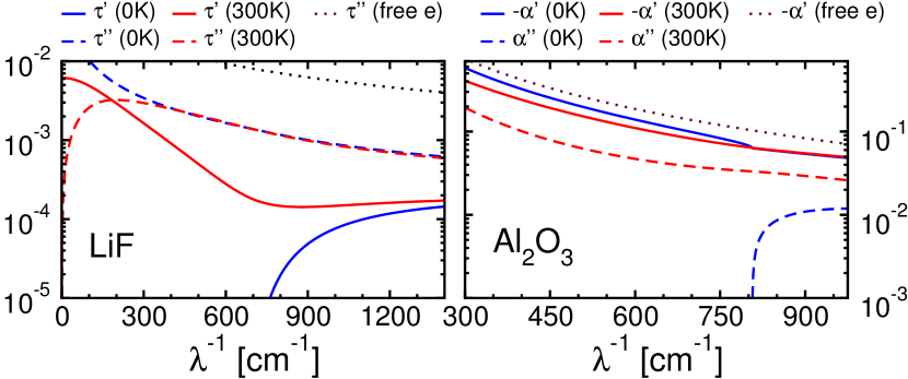
The charge effect on scattering is encoded in the surface conductivity for and the bulk conductivity for which enter through the dimensionless surface conductivity or the polarisability into the scattering coefficients. Figure 14 shows for LiF and the polarisability for for Al2O3 as a function of the inverse wavelength . They turn out to be small even for a highly charged particle with cm-2 (corresponding to cm-3 for and m). Compared to a free electron gas where (implying and ), the electron-phonon coupling reduces and considerably. For , () for cm-1, the inverse wavelength of the surface phonon ( cm-1, the inverse wavelength of the bulk LO phonon) since light absorption is only possible above the surface (bulk LO) phonon frequency. At room temperature and still outweigh and . The temperature effect on is less apparent for cm-1 than for but for cm-1 a higher temperature lowers considerably.
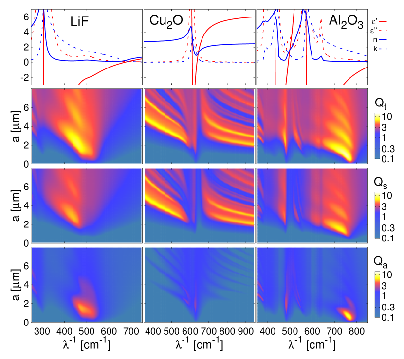
We now turn to the scattering properties of the sphere. For LiF and Al2O3 one or two phonon modes dominate the dielectric constant. Far above the highest TO phonon mode ( cm-1 for LiF and cm-1 for Al2O3) the refractive index is real, relatively small and does not vary strongly with frequency. In this regime a micron sized grain would give rise to a typical Mie plot exhibiting interference and ripples which are due to the complicated functional form of and and not due to the underlying dielectric constant. Surplus electrons would moreover not alter the extinction behaviour in this region because and .
However, immediately above the TO phonon resonance in , and . This allows for anomalous optical resonances which are sensitive to small variations of and also to and . They are due to resonant excitation of transverse surface modes of the sphere FK68 and have been first identified for metallic particles where they lie in the ultraviolet TL06 ; Tribelsky11 . For a dielectric the TO phonon induces them. Fig. 15 shows the dielectric constant , the refractive index as well as the extinction , scattering , and absorption efficiency for LiF, Cu2O and Al2O3 particles as a function of and the particle radius . For LiF and Al2O3 we find a clearly resolved series of optical resonances. For the smaller particles they are due to absorption while for larger particles they are scattering resonances. The crossover between scattering and absorption occurs in the first resonance. For comparison, we display in Fig. 15 also results for Cu2O particles which do not show clearly resolved resonances. For this material but is not sufficiently small to allow for sharp resonances. Nevertheless for submicron-sized particles a small extinction resonance due to absorption can be identified near cm-1.
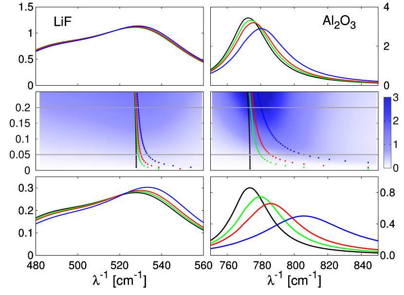
The extinctions resonances are blue-shifted with increasing particle charge HBF12b . This effect is most significant for small particles. Fig. 16 shows the small particle tail of the lowest extinction resonance for LiF and Al2O3. The main panel shows the extinction efficiency as a function of the particle radius and the inverse wavelength for cm-1 (LiF) or (Al2O3). Superimposed is the extinction maximum for several values of and corresponding . The top and bottom panel show the lineshape of the extinction resonance for m and m. For both materials the surplus electrons lead to a blue-shift of the resonance.
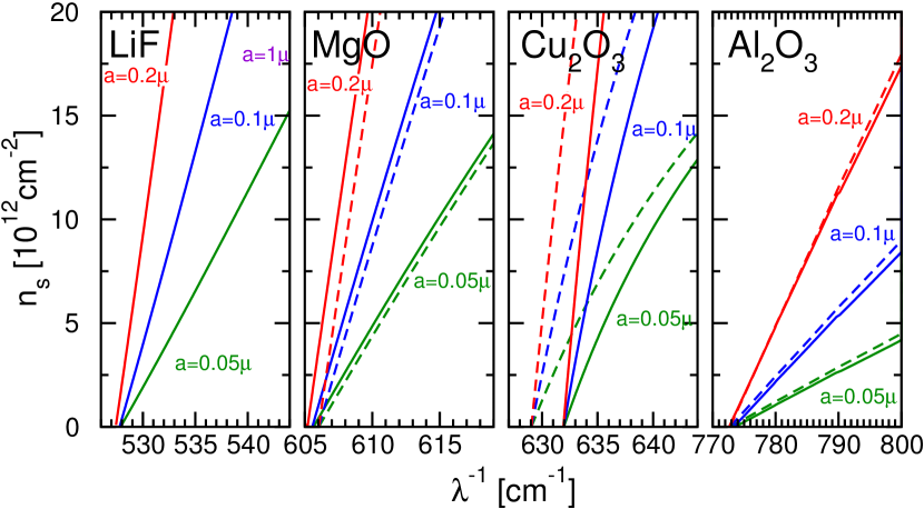
For submicron-sized particles where the resonance shift is most significant . In this small particle limit we can expand the scattering coefficients for small . To ensure that in the limit of an uncharged surface, that is, for , and converge to their known small expansions Stratton41 , we substitute prior expanding the scattering coefficients. Up to this yields and only contributes. Then the extinction efficiency reads
| (61) |
where we have restored . Excess charges enter either by () or (). For this gives the limit of Rayleigh scattering. The resonance is located at wavenumbers where
| (62) |
| (63) |
and has a Lorentzian shape provided and (or ) vary only negligibly near the resonance wavelength. Figure 16 confirms the Lorentzian lineshape for Al2O3. For LiF, however, has a hump (see Fig. 15) close to the resonance due to a second TO phonon mode which is much weaker than the dominant TO phonon. This leads to the deviation form the Lorentzian lineshape.
For an uncharged surface the resonance is at for which . For the shift of the resonance is proportional to and thus to , provided is well approximated linearly in and does not vary significantly near . In this case, we substitute in (62) the expansions and where and . Then the resonance is located at . For the resonance is located at where .
The proportionality of the resonance shift to for LiF and for Al2O3 can also be seen in Fig. 17 where we plot on the abscissa the shift of the extinction resonance arising from the surface electron density (or corresponding bulk electron density) given on the ordinate for LiF, MgO () as well as Cu2O and Al2O3 (). Both bulk and surface electrons lead qualitatively to the same resonance shift. Note that even for Cu2O which does not show clearly resolved extinction resonance a shift is discernible. The most promising candidate for an optical charge measurement is Al2O3 where the shift is strongest.
To illustrate the similarity of bulk and surface electron effects we consider the resonance condition (62) or (63) for free electrons, which then becomes
| (64) |
for and
| (65) |
for , where is the number of electrons on the sphere. The effect of surface electrons is weaker by a factor of . The factor can be understood as a geometric factor as only the parallel component of the electric field acts on the spherically confined electron gas. Most important, however, the fact that and enter the resonance condition on the same footing shows that the resonance blueshift is in the first place an electron density effect on the polarizability of the grain. We therefore expect the shift to prevail also for a more complex electron distribution on the grain between the two limiting cases of a surface and a homogeneous bulk charge.
Our results suggest to use the shift of the extinction resonance to determine the particles charge. This requires the use of particles with a strong TO phonon resonance in the dielectric constant which leads to and above the TO phonon frequency. The resoance shift is found for particles with surface (, e.g. MgO, LiF) as well as bulk excess electrons ( e.g. Al2O3). For dusty plasmas an optical charge diagnostic can be rather attractive because established methods for measuring the particle charge CJG11 ; KRZ05 ; TLA00 require plasma parameters which are not precisely known whereas the charge measurement by Mie scattering does not (see Fig. 18). Particles showing the resonance shift could be employed as minimally invasive electric probes, which collect electrons depending on the local plasma environment. Determining their charge from Mie scattering and the forces acting on them by conventional means CJG11 ; KRZ05 ; TLA00 would then allow to extract the local plasma parameters. Moreover, the Mie signal would provide a charge diagnostic for nanodust GCK12 , which is too small and light for traditional charge measurements.
5 Summary
This chapter introduces a microscopic modelling of the plasma wall which complements traditional sheath models by an interface region—the ESL. In this model the negative charge on the plasma boundary is treated as a wall-thermalised electron distribution minimising the grand canonical potential and satisfying Poisson’s equation. Its boundary with the plasma sheath is determined by a force balance between the attractive image potential and the repulsive sheath potential and lies in front of the crystallographic interface. Depending on the electron affinity , that is the offset of the conduction band minimum to the potential in front of the surface, two scenarios for the wall-bound electrons are realised. For (e.g. MgO, LiF) electrons do not penetrate into the solid but are trapped in the image states in front of the surface where they form a quasi two-dimensional electron gas. For (e.g. SiO2, Al2O3) electrons penetrate into the conduction band where they form an extended space charge.
These different scenarios are also reflected in the electron physisorption at the wall. For electrons from the plasma cannot penetrate into the solid. They are trapped in the image states in front of the surface. The transitions between unbound and bound states are due to surface vibrations. In this case the sticking coefficient for electrons is relatively small, typically on the order of . For electron physisorption takes place in the conduction band. For this case sticking coefficients and desorption times have not been calculated yet but in view of the more efficient scattering with bulk phonons, responsible for electron energy relaxation in this case, we expect them to be larger than for the case of . This indicates that the electron affinity should be an important parameter for the charging-up of plasma walls. In particular dusty plasmas offer the possibility to study experimentally the charge-up of dust grains depending on this parameter.
Our microscopic model can also be applied to study the optical properties of the wall-bound electrons on a dust particle. Surplus electrons affect the polarisability of the dust particle by their surface () or bulk conductivity (). This leads to a blue-shift of an extinction resonance in the infrared for negatively charged dust particles. This effect offers an optical way to measure the particle charge which, unlike tradition charge measurements, does not require the plasma parameters at the position of the particle.
Acknowledgements.
This work was supported by Deutsche Forschungsgemeinschaft through SFB-TR 24.References
- (1) R.N. Franklin, Plasma phenomena in gas discharges (Clarendon Press, Oxford, 1976)
- (2) C.J. Wagner, P.A. Tschertian, J.G. Eden, Appl. Phys. Lett. 97, 134102 (2010)
- (3) H. Baumgartner, D. Block, M. Bonitz, Contrib. Plasma Phys. 49, 281 (2009)
- (4) A. Piel, O. Arp, D. Block, I. Pilch, T. Trottenberg, S. Kaeding, A. Melzer, H. Baumgartner, C. Henning, M. Bonitz, Plasma Phys. Control. Fusion 49, 281 (2008)
- (5) V.E. Fortov, A.V. Ivlev, S.A. Khrapak, A.G. Khrapak, G.E. Morfill, Phys. Rep. 421, 1 (2005)
- (6) J. Berndt, E. Kovačević, V. Selenin, I. Stefanović, J. Winter, Plasma Sources Sci. Technol. 15, 18 (2006)
- (7) Y.B. Golubovskii, V.A. Maiorov, J. Behnke, J.F. Behnke, J. Phys. D: Appl. Phys 35, 751 (2002)
- (8) H.E. Wagner, Y.V. Yurgelenas, R. Brandenburg, Plasma Phys. Control. Fusion 47, B641 (2005)
- (9) R. Brandenburg, V.A. Maiorov, Y.B. Golubovskii, H.E. Wagner, J. Behnke, J.F. Behnke, J. Phys. D: Appl. Phys 38, 2187 (2005)
- (10) L. Stollenwerk, J.G. Laven, H.G. Purwins, Phys. Rev. Lett. 98, 255001 (2007)
- (11) M. Bogaczyk, R. Wild, L. Stollenwerk, H.E. Wagner, J. Phys. D: Appl. Phys 46, 465202 (2012)
- (12) M. Bogaczyk, S. Nemschokmichal, R. Wild, L. Stollenwerk, R. Brandenburg, J. Meichsner, H.E. Wagner, Contrib. Plasma Phys. 52, 847 (2012)
- (13) K.H. Becker, K.H. Schoenbach, J.G. Eden, J. Phys. D: Appl. Phys 39, R55 (2006)
- (14) M.J. Kushner, J. Phys. D: Appl. Phys 38, 1633 (2005)
- (15) U. Kogelschatz, Plasma Chemistry and Plasma Processing 23, 1 (2003)
- (16) P.A. Tschertian, C.J. Wagner, T.L. Houlahan, B. Li, D.J. Sievers, J.G. Eden, Contrib. Plasma Phys. 51, 889 (2011)
- (17) R. Dussart, L. Overzet, P. Lefaucheux, T. Dufour, M. Kulsreshath, M. Mandra, T. Tillocher, O. Aubry, S. Dozias, P. Ranson, J. Lee, , M. Goeckner, Eur. Phys. J. D 60, 601 (2010)
- (18) K.G. Emeleus, J.R.M. Coulter, Int. J. Electronics 62, 225 (1987)
- (19) J.F. Behnke, T. Bindemann, H. Deutsch, K. Becker, Contrib. Plasma Phys. 37, 345 (1997)
- (20) R.L. Heinisch, F.X. Bronold, H. Fehske, Phys. Rev. B 85, 075323 (2012)
- (21) F. Stern, Phys. Rev. B 17, 5009 (1978)
- (22) E.E. Tkharev, A.L. Danilyuk, Vacuum 35, 183 (1985)
- (23) M.A. Lieberman, A.J. Lichtenberg, Principles of plasma discharges and materials processing (Wiley-Interscience, New York, 2005)
- (24) K.U. Riemann, J. Phys. D: Appl. Phys 24, 493 (1991)
- (25) J.D. Jackson, Classical electrodynamics (Wiley, New York, 1998)
- (26) J.B. Cui, J. Ristein, L. Ley, Phys. Rev. Lett. 81, 429 (1998)
- (27) F. Maier, J. Ristein, L. Ley, Phys. Rev. B 64, 165411 (2001)
- (28) F. Stern, S.D. Sarma, Phys. Rev. B 30, 840 (1984)
- (29) H. Lüth, Solid Surfaces, Interfaces and Thin Films (Springer-Verlag, 1992)
- (30) W. Kohn, L.J. Sham, Phys. Rev. 140A, 1133 (1965)
- (31) N.D. Mermin, Phys. Rev. 137A, 1441 (1965)
- (32) K.G. Emeleus, J.R.M. Coulter, IEE Proceedings 135, 76 (1988)
- (33) F.X. Bronold, H. Fehske, R.L. Heinisch, J. Marbach, Contrib. Plasma Phys. 52, 859 (2012)
- (34) R.L. Heinisch, F.X. Bronold, H. Fehske, Phys. Rev. B 81, 155420 (2010)
- (35) R.L. Heinisch, F.X. Bronold, H. Fehske, Phys. Rev. B 82, 125408 (2010)
- (36) R.L. Heinisch, F.X. Bronold, H. Fehske, Phys. Rev. B 83, 195407 (2011)
- (37) Z.W. Gortel, H.J. Kreuzer, R. Teshima, Phys. Rev. B 22, 5655 (1980)
- (38) H.J. Kreuzer, Z.W. Gortel, Physisorption Kinetics (Springer Verlag, Berlin, 1986)
- (39) G. Iche, P. Noziéres, J. Phys. (Paris) 37, 1313 (1976)
- (40) W. Brenig, Z. Phys. B 48, 127 (1982)
- (41) E. Evans, D.L. Mills, Phys. Rev. B 8, 4004 (1973)
- (42) G. Barton, J. Phys. C 14, 3975 (1981)
- (43) B. Bendow, S.C. Ying, Phys. Rev. B 7, 622 (1973)
- (44) J. Carstensen, H. Jung, F. Greiner, A. Piel, Phys. Plasmas 18, 033701 (2011)
- (45) S.A. Khrapak, S.V. Ratynskaia, A.V. Zobnin, A.D. Usachev, V.V. Yaroshenko, M.H. Thoma, M. Kretschmer, H. Hoefner, G.E. Morfill, O.F. Petrov, V.E. Fortov, Phys. Rev. E 72, 016406 (2005)
- (46) E.B. Tomme, D.A. Law, B.M. Annaratone, J.E. Allen, Phys. Rev. Lett. 85, 2518 (2000)
- (47) F. Greiner, J. Carstensen, N. Koehler, I. Pilch, H. Ketelsen, S. Knist, A. Piel, Plasma Sources Sci. Technol. 21, 065005 (2012)
- (48) C.F. Bohren, D.R. Huffman, Absorption and Scattering of Light by small particles (Wiley, 1983)
- (49) J. Klačka, M. Kocifaj, Progress in Electromagnetics Research 109, 17 (2010)
- (50) J. Klačka, M. Kocifaj, J. of Quantitative Spectroscopy and Radiative Transfer 106, 170 (2007)
- (51) C.F. Bohren, A.J. Hunt, Can. J. Phys. 55, 1930 (1977)
- (52) M. Rohlfing, N.P. Wang, P. Krueger, J. Pollmann, Phys. Rev. Lett. 91, 256802 (2003)
- (53) B. Baumeier, P. Krueger, J. Pollmann, Phys. Rev. B 76, 205404 (2007)
- (54) J.A. Stratton, Electromagnetic theory (McGraw-Hill, 1941)
- (55) E.T. Whittaker, G.N. Watson, A course of modern analysis (Cambridge University Press, 1927)
- (56) M. Kato, A. Ishii, Appl. Surf. Sci. 85, 69 (1995)
- (57) W. Götze, P. Wölfle, Phys. Rev. B 6, 1226 (1972)
- (58) R.L. Heinisch, F.X. Bronold, H. Fehske, Phys. Rev. Lett. 109, 243903 (2012)
- (59) G.D. Mahan, Many-particle physics (Plenum, 1990). P. 703-708
- (60) R. Fuchs, K.L. Kliewer, J. Opt. Soc. Am. 58, 319 (1968)
- (61) M.I. Tribelsky, B.S. Luk’yanchuk, Phys. Rev. Lett. 97, 263902 (2006)
- (62) M.I. Tribelsky, Europhys. Lett. 94, 14004 (2011)