Multimode plasmon excitation and in-situ analysis in top-down fabricated nanocircuits
Abstract
We experimentally demonstrate synthesis and in-situ analysis of multimode plasmonic excitations in two-wire transmission lines supporting a symmetric and an antisymmetric eigenmode. To this end we irradiate an incoupling antenna with a diffraction-limited excitation spot exploiting a polarization- and position-dependent excitation efficiency. Modal analysis is performed by recording the far-field emission of two mode-specific spatially separated emission spots at the far end of the transmission line. To illustrate the power of the approach we selectively determine the group velocities of symmetric and antisymmetric contributions of a multimode ultrafast plasmon pulse.
pacs:
42.79.Gn, 73.20.Mf, 84.40.Az, 84.40.BaMiniaturization of functional optical circuits is hampered by the diffraction-limited modal profiles of dielectric waveguides Yariv and Yeh (2007). In contrast, plasmonic modes supported by noble-metal nanostructures offer subwavelength confinement Novotny and Hafner (1994); Takahara et al. (1997); Barnes et al. (2003) and therefore promise the realization of nanometer-scale integrated optical circuitry with well-defined functionality Ozbay (2006); Gramotnev and Bozhevolnyi (2010). While single-mode operation is a design goal for dielectric waveguides, in plasmonic nanocircuits multimode interference could lead to enhanced functionality based on the control of near-field intensity patterns Stockman et al. (2002); Sukharev and Seideman (2006); Tuchscherer et al. (2009).
Previous work towards the realization of optical nanocircuits relied on chemically grown single-wire waveguides pioneered by Ditlbacher et al. Ditlbacher et al. (2005). In such systems the plasmon excitation and emission efficiencies depend on the wire diameter, which at the same time also determines the spectrum of modes and their respective dispersion relations. In addition, structural uncertainties, such as the uncontrolled shape of the end facets, have a strong influence on the far-field excitation and emission properties of different modes Li et al. (2010); Shegai et al. (2011); Song et al. (2011). By combining careful selection and micromanipulation of chemically grown nanowires, indeed prototypes of optical nanocircuitry have been demonstrated in which multimode interference is exploited Fang et al. (2010); Wei et al. (2011).
Despite these achievements, it is a necessary next step towards advanced plasmonic nanodevices to obtain independent control over light coupling and propagation in optical nanocircuits by a deterministic synthesis of multimodal excitations. The existence of a transverse and a longitudinal mode in chains of closely spaced plasmonic nanoparticles Quinten et al. (1998); Maier et al. (2003) led to a proposal of deterministic coherent control of a routing functionality in a branched particle-chain waveguide circuit Tuchscherer et al. (2009). Later on, easier to fabricate metal-insulator-metal (MIM)-type waveguides, such as grooves and channels Bozhevolnyi et al. (2005) were applied e.g., to implement logic operations, albeit via single-mode interference Fu et al. (2012).
To obtain more flexibility and control in terms of excitation schemes and available modes, two-wire transmission lines (TWTLs) offering a symmetric and an antisymmetric mode Ly-Gagnon et al. (2012), are a logical extension of both single-wire and MIM concepts. However, experiments so far have only considered the antisymmetric modeKrenz et al. (2010); Schnell et al. (2011); Ly-Gagnon et al. (2012). Importantly, TWTLs can be combined with linear dipole antennas to tailor the in- and outcoupling of light Huang et al. (2009); Wen et al. (2009); Krenz et al. (2010); Schnell et al. (2011).
Here, we use plasmonic nanocircuits Huang et al. (2009) consisting of an optimized incoupling antenna (generator), a transmission line with a mode-dependent characteristic impedance, and a mode detector (load). The structures are fabricated by focused ion beam (FIB) milling of single-crystalline gold flakes and therefore structural detail and plasmon propagation are not limited by the grain boundaries of multi-crystalline gold films Huang et al. (2010a); Ditlbacher et al. (2005). We show that by controlling polarization and exact position of a near-infrared laser focus with respect to the antenna, any superposition of TWTL modes can be launched and analyzed by a single-shot in-situ far-field read-out of the mode detector. As a first application, we selectively determine group velocities and time delays of pure-mode contributions of a multimode ultrafast TWTL plasmon pulse.
Control of multimodal excitations provides advanced circuit functionality, e.g. through deterministic coherent control of nanooptical fields as described in Tuchscherer et al. (2009) where multimode operation is a necessity. Such control of confined fields can also be used for the implementation of nonlinear optical switching effects and the controlled interaction of guided modes with single quantum emitters Akimov et al. (2007); Kolesov et al. (2009).
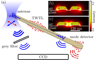
Plasmonic nanocircuits [Fig. 1 (a)] consisting of an incoupling antenna, a TWTL, and a mode detector, were fabricated by FIB milling (FEI company, Helios NanoLab) of a large single-crystalline gold flake (38 nm thickness) deposited on a cover glass Huang et al. (2010a). For the chosen dimensions only two TWTL modes with considerable propagation length (>2 m) exist. The transverse modal profile of any multimodal excitation propagating along the TWTL at a fixed position therefore is a superposition of these two eigenmodes after transients have expired Huang et al. (2009).
| mode property | symmetric | antisymmetric |
|---|---|---|
| 480 | 434 | |
| 2628 | 1892 | |
| 1.26 | 1.16 |
Figures 1 (b,c) show the simulated transverse eigenmode profiles of the symmetric and the antisymmetric mode for a TWTL consisting of a pair of gold wires with rounded upper corners on glass elevations above a glass half space (Lumerical Solutions Inc., MODE Solutions). The false color scale represents the time-averaged near-field intensity. The corresponding eigenmode properties are summarized in Table 1. The longer propagation length, longer effective wavelength, as well as higher group velocity observed for the symmetric mode are consistent with its lower field confinement.
The mode detector attached to the far end of the TWTL can be read out via a diffraction-limited far-field measurement and therefore provides direct in-situ feedback on the actual modal composition. Its operation principle relies on the different interaction of symmetric and antisymmetric modes with different types of TWTL discontinuities. Due to a field node in the gap the symmetric eigenmode is not affected by a termination of the gap while it is strongly reflected and radiated at a complete termination of the circuit. The antisymmetric eigenmode exhibits a field maximum in the gap and is thus strongly reflected and radiated as soon as the gap is terminated. A sequence of a gap shortcut followed by a complete termination of the TWTL therefore acts as a mode detector by spatially separating the respective emission spots.
Figure 2 (a,b) show scanning electron micrographs (SEM) of a plasmonic nanocircuit featuring a 4 m long TWTL visualizing the rounded shape of the TWTL wires caused by secondary sputtering processes during FIB milling. Figures 2 (c,d) show far-field FDTD simulations of the mode detector interacting with either of the two eigenmodes.
The 1 m spacing between the discontinuities results in two clearly separated emission spots whose intensities are proportional to the amplitudes of the respective eigenmode contributions. The emission is polarized parallel to the wire axis for the symmetric [Fig. 2 (c)] and perpendicular for the antisymmetric mode emission spot [Fig. 2 (d)]. For a quantitative determination of the power in each mode the respective radiation efficiencies of the two emission points have to be taken into account. As a figure of merit (FOM) for the ability of the mode detector to separate modal contributions we define for an incoming pure symmetric (antisymmetric) mode plasmon , where is the emission intensity at the symmetric (antisymmetric) emission spot. Perfect mode selectivity corresponds to . Due to the small amount of scattered light at the position of the mode detector we achieve typical figure of merits of 0.98 in experiments and in simulations.
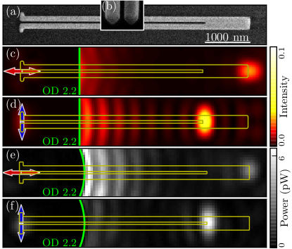
In order to experimentally characterize the launching and emission of plasmon excitations, the cover glass supporting the nanocircuit is mounted onto a home-built inverted microscope setup. An oil immersion microscope objective (Leica, 1.30 NA, , PL Fluotar 100x) is used to focus a linearly polarized laser beam ( = 830 nm, 12 nm FWHM spectral linewidth, 80 MHz repetition rate, 100 nW average power measured in front of the objectives back aperture, NKT Photonics, SuperK Power with SpectraK AOTF) via a -plate (Foctec, AWP210H NIR) to a diffraction-limited (390 nm diameter) spot at the glass/air interface. Once the spot is overlapped with the incoupling antenna of a TWTL structure, plasmons are excited and subsequently re-emitted at the far end of the structure. The same objective is used to image the emission spots onto a CCD camera (Andor, DV887AC-FI EMCCD) via a 50/50 nonpolarizing beamsplitter (Thorlabs, CM1-BS013). In order to avoid saturation of the CCD, the strong reflection of the excitation spot is suppressed by a small beam block (OD 2.2) introduced in an intermediate image plane. The exact position of the excitation spot can be adjusted with nm-precision by moving the sample using a piezo translation stage (Physik Instrumente, P-527). The principle of the experiment is sketched in Fig. 1 (a). Figures 2 (e) and (f) show far-field images of the structure being excited at the antenna and re-emitting light at the mode detector structure for excitation polarizations parallel (e) and perpendicular (f) to the TWTL. To launch the antisymmetric mode in (f) the polarization was rotated by 90∘ while the excitation spot was kept fixed. This demonstrates the possibility to excite a well-defined superposition of both modes simply by adjusting the laser polarization. It is interesting to observe that not only the positions of the far-field emission spots match very well the simulations in Figs. 2 (c,d) but also the respective spot shapes.
The excitation efficiency of both TWTL modes can be engineered by utilizing an incoupling structure that links the field profile of the excitation beam to the modal profiles of the TWTL. Here we use a simple dipole antenna where the length and width of the antenna arms influence the antenna impedance and therefore the transfer of power to the respective waveguide mode Huang et al. (2009). In Fig. 3 we plot both the experimentally determined and simulated incoupling efficiencies into either TWTL mode as a function of the overall antenna length (350 - 550 nm, the 290 nm simulation corresponds to the “no-antenna” – “wire-only” case) for a fixed antenna width (80 nm). In simulations, the mode-specific incoupling efficiency is obtained by evaluating a mode overlap integral at a distance from the antenna where direct influence of the excitation beam and transients can be neglected (i.e., 2.5 m from the antenna). By taking into account the simulated decay length (see Table 1) this power is then extrapolated towards the incoupling antenna position. Consequently, reads as
where is the power in the respective mode at position along the wire, the laser power and the intensity decay length of the mode. For polarization parallel to the TWTL (Fig. 3, red dashed line) the incoupling efficiency of the symmetric mode decreases from a large value of >30% for the case without antenna to a narrow minimum of <5% at around 425 nm overall antenna length and then largely recovers for a further increase of the antenna length. Excitation of the antisymmetric mode is symmetry forbidden for this polarization unless the focus is displaced (see below). For a polarization perpendicular to the TWTL (Fig. 3, blue solid line) the behavior is quite the opposite. Without antenna the antisymmetric mode can hardly be excited (<2% excitation efficiency). By increasing the antenna length to about 425 nm the incoupling efficiency reaches a maximum of almost 30% and then decreases towards another minimum for even longer antennas. For perpendicular polarization, coupling to the symmetric mode is symmetry forbidden.
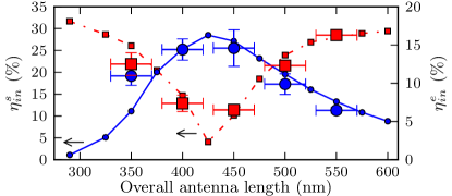
To experimentally verify these predictions, 2 nominally identical arrays consisting of 5 nanocircuits with scanned antenna lengths have been fabricated. By taking into account the damping of the wire (see Table 1) and the radiation efficiencies of the mode detector emission spots, the power in each mode at the antenna position can be extrapolated. We plot the experimental incoupling efficiency (Fig. 3, large symbols), defined as
where is the integrated emitted power at an emission spot, the excitation power measured in front of the objective, the radiation efficiency of either emission spot corrected by the collection solid angle of the objective lens (about 25% for both modes), the length of the TWTL, and the simulated decay length. While the experimental data very well reproduce the general trend the absolute experimental values for the incoupling efficiency are smaller by about a factor of 2. Such a deviation can be caused by experimental decay lengths that are about 25% shorter than predicted by simulations. The reason for such deviations is unclear but effects like surface scattering of electrons likely contribute.
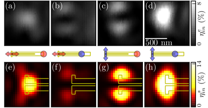
So far we have assumed an excitation focal spot perfectly centered on the incoupling antenna (neglecting small displacements along the TWTL) leading to the excitation of pure modes for the two fundamental polarizations. We test the stability of such a configuration by recording the excitation efficiencies into both modes for parallel and perpendicular polarization as a function of beam displacements. Breaking the symmetry, such displacements lead to a significant increase in the excitation efficiency of the respective symmetry forbidden modes Huang et al. (2010b). Figures 4 (a–d) show excitation efficiency maps for both fundamental polarizations obtained by recording the integrated emission intensity at the respective positions of the mode detector as a function of excitation spot position over a range of m. For parallel (perpendicular) polarization the maps feature a single connected region roughly centered on the incoupling antenna if the emission is recorded at the corresponding emission position of the symmetric (antisymmetric) mode. If the “wrong” mode detector port emission is recorded, then, despite the seemingly wrong polarization, the corresponding modes can still be detected if the beam is displaced perpendicular to the TWTL axis. This results in two disconnected areas in the excitation efficiency maps which are reproduced by FDTD simulations [Figs. 4 (e–h)]. We conclude that excitation of pure modes requires both control of the polarization and nanometer-scale precision for the positioning of the excitation spot. We further conclude that both degrees of freedom, polarization and focal spot position, can be used to synthesize linear combinations of pure modes.
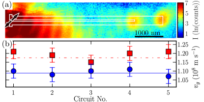
As an application we demonstrate the selective determination of the group velocities of symmetric and antisymmetric contributions of a multimode ultrafast plasmon pulse. We create such a plasmon pulse using a well-positioned excitation spot polarized at 45∘ with respect to the TWTL [Fig. 5 (a)]. The experiment is performed using ultrashort pulses (800 nm central wavelength, 53 nm FWHM, 80 MHz repetition rate, 2 nW average excitation power) on a dedicated setup Rewitz et al. (2012a, b) using one of the TWTL arrays of Fig. 3. A time-averaging detector imaging the mode detector records about equal intensities for both ports. However, since both modes travel at different group velocities, the symmetric and the antisymmetric pulse contributions actually arrive at their ports at slightly different instants after correcting for the total propagation distance. Such minute time delays as well as absolute propagation times can be measured using spectral-interference microscopy Rewitz et al. (2012b). From the determined propagation times we calculate the respective modal group velocities. The results are displayed in Fig. 5 (b) and compared to simulated values. Within the error margins quantitative agreement between experiment and theory is found and the small differences in the modal group velocities can be clearly resolved. As expected, the less-confined symmetric mode is closer to the free-space propagation speed (about 10% faster than the antisymmetric mode). No systematic influence of the antenna length on the pulse propagation time is observed.
We conclude that near-infrared plasmon excitations (cw and ultrafast) in top-down fabricated single-crystalline gold TWTL nanocircuits can be prepared in deterministic eigenmode superpositions by positioning a tightly focused laser beam with respect to the incoupling antenna attached to the TWTL and by adjusting its polarization. Modal analysis is performed in-situ by means of a mode detector structure that is read out by a single-shot far-field measurement providing a direct feedback on the modal composition. Finally, we use these abilities to study the propagation of a deterministic ultrashort multimodal plasmon pulse by the separate measurement of the group velocities of its eigenmode contributions.
Acknowledgements.
The authors gratefully acknowledge Thorsten Feichtner, Monika Emmerling, and Monika Pawłowska for 3D artwork, for fabricating the beam block, and fruitful discussions, respectively as well as the DFG for financial support within the Priority Program “Ultrafast Nanooptics” (SPP 1391).References
- Yariv and Yeh (2007) A. Yariv and P. Yeh, Photonics : Optical Electronics in Modern Communications, 6th ed. (Oxford University Press, New York, 2007).
- Novotny and Hafner (1994) L. Novotny and C. Hafner, Phys. Rev. E 50, 4094 (1994).
- Takahara et al. (1997) J. Takahara, S. Yamagishi, H. Taki, A. Morimoto, and T. Kobayashi, Optics Letters 22, 475–477 (1997).
- Barnes et al. (2003) W. L. Barnes, A. Dereux, and T. W. Ebbesen, Nature 424, 824 (2003).
- Ozbay (2006) E. Ozbay, Science 311, 189 (2006).
- Gramotnev and Bozhevolnyi (2010) D. K. Gramotnev and S. I. Bozhevolnyi, Nat. Photon. 4, 83 (2010).
- Stockman et al. (2002) M. I. Stockman, S. V. Faleev, and D. J. Bergman, Phys. Rev. Lett. 88, 067402 (2002).
- Sukharev and Seideman (2006) M. Sukharev and T. Seideman, Nano Lett. 6, 715 (2006).
- Tuchscherer et al. (2009) P. Tuchscherer, C. Rewitz, D. V. Voronine, F. J. García de Abajo, W. Pfeiffer, and T. Brixner, Opt. Express 17, 14235 (2009).
- Ditlbacher et al. (2005) H. Ditlbacher, A. Hohenau, D. Wagner, U. Kreibig, M. Rogers, F. Hofer, F. R. Aussenegg, and J. R. Krenn, Phys. Rev. Lett. 95, 257403 (2005).
- Li et al. (2010) Z. Li, K. Bao, Y. Fang, Y. Huang, P. Nordlander, and H. Xu, Nano Lett. 10, 1831 (2010).
- Shegai et al. (2011) T. Shegai, V. D. Miljković, K. Bao, H. Xu, P. Nordlander, P. Johansson, and M. Käll, Nano Lett. 11, 706 (2011).
- Song et al. (2011) M. Song, A. Bouhelier, P. Bramant, J. Sharma, E. Dujardin, D. Zhang, and G. Colas-des Francs, ACS Nano 5, 5874 (2011).
- Fang et al. (2010) Y. Fang, Z. Li, Y. Huang, S. Zhang, P. Nordlander, N. J. Halas, and H. Xu, Nano Lett. 10, 1950–1954 (2010).
- Wei et al. (2011) H. Wei, Z. Wang, X. Tian, M. Käll, and H. Xu, Nat. Comm. 2, 387 (2011).
- Quinten et al. (1998) M. Quinten, A. Leitner, J. R. Krenn, and F. R. Aussenegg, Optics Letters 23, 1331 (1998).
- Maier et al. (2003) S. A. Maier, P. G. Kik, H. A. Atwater, S. Meltzer, E. Harel, B. E. Koel, and A. A. G. Requicha, Nature Materials 2, 229 (2003).
- Bozhevolnyi et al. (2005) S. I. Bozhevolnyi, V. S. Volkov, E. Devaux, and T. W. Ebbesen, Phys. Rev. Lett. 95, 046802 (2005).
- Fu et al. (2012) Y. Fu, X. Hu, C. Lu, S. Yue, H. Yang, and Q. Gong, Nano Lett. 12, 5784 (2012).
- Ly-Gagnon et al. (2012) D.-S. Ly-Gagnon, K. C. Balram, J. S. White, P. Wahl, M. L. Brongersma, and D. A. Miller, Nanophotonics 1 (2012), 10.1515/nanoph-2012-0002.
- Krenz et al. (2010) P. M. Krenz, R. L. Olmon, B. A. Lail, M. B. Raschke, and G. D. Boreman, Opt. Express 18, 21678 (2010).
- Schnell et al. (2011) M. Schnell, P. Alonso-González, L. Arzubiaga, F. Casanova, L. E. Hueso, A. Chuvilin, and R. Hillenbrand, Nat. Photon. 5, 283 (2011).
- Huang et al. (2009) J.-S. Huang, T. Feichtner, P. Biagioni, and B. Hecht, Nano Lett. 9, 1897 (2009).
- Wen et al. (2009) J. Wen, S. Romanov, and U. Peschel, Opt. Express 17, 5925 (2009).
- Huang et al. (2010a) J.-S. Huang, V. Callegari, P. Geisler, C. Brüning, J. Kern, J. C. Prangsma, X. Wu, T. Feichtner, J. Ziegler, P. Weinmann, M. Kamp, A. Forchel, P. Biagioni, U. Sennhauser, and B. Hecht, Nat. Comm. 1, 150 (2010a).
- Akimov et al. (2007) A. V. Akimov, A. Mukherjee, C. L. Yu, D. E. Chang, A. S. Zibrov, P. R. Hemmer, H. Park, and M. D. Lukin, Nature 450, 402 (2007).
- Kolesov et al. (2009) R. Kolesov, B. Grotz, G. Balasubramanian, R. J. Stöhr, A. A. L. Nicolet, P. R. Hemmer, F. Jelezko, and J. Wrachtrup, Nature Physics 5, 470 (2009).
-
Inc. (2012)
L. Inc., “Imaging | FDTD solutions knowledge
base,” http://docs.lumerical.com/en/fdtd/microscopy
_imaging.html (2012). - Huang et al. (2010b) J.-S. Huang, J. Kern, P. Geisler, P. Weinmann, M. Kamp, A. Forchel, P. Biagioni, and B. Hecht, Nano Lett. 10, 2105 (2010b).
- Rewitz et al. (2012a) C. Rewitz, T. Keitzl, P. Tuchscherer, J.-S. Huang, P. Geisler, G. Razinskas, B. Hecht, and T. Brixner, Nano Lett. 12, 45 (2012a).
- Rewitz et al. (2012b) C. Rewitz, T. Keitzl, P. Tuchscherer, S. Goetz, P. Geisler, G. Razinskas, B. Hecht, and T. Brixner, Opt. Express 20, 14632 (2012b).