Observation of angle-dependent transmission of Dirac electrons in graphene heterojunctions
The relativistic nature of charge carriers in graphene is expected to lead to an angle-dependent transmission through a potential barrier, where Klein tunneling involves annihilation of an electron and a hole at the edges of the barrier. The signatures of Klein tunneling have been observed in gated graphene devices, but the angle dependence of the transmission probability has not been directly observed. Here we show measurements of the angle-dependent transmission through quasi-ballistic graphene heterojunctions with straight and angled leads, in which the barrier height is controlled by a shared gate electrode. Using a balanced differential measurement technique, we isolate the angle-dependent contribution to the resistance from other angle-insensitive, gate-dependent and device-dependent effects. We find large oscillations in the transmission as a function of the barrier height in the case of Klein tunneling at a 450 angle, as compared to normal incidence. Our results are consistent with the model that predicts oscillations of the transmission probability due to interference of chiral carriers in a ballistic barrier. The observed angle dependence is the key element behind focusing of electrons and the realization of a Veselago lens in graphene.
Charge carriers in graphene behave like massless, relativistic particles gr_1 ; gr_3 ; g_2 ; g_3 , characterized by chirality which arises from the existence of two interpenetrating sublattices in the hexagonal crystal structure of graphene. Due to the chiral nature of the charge carriers, back scattering by impurities is forbidden back_1 ; back_2 , giving rise to unusual effects in graphene p-n-p junctions such as Klein tunneling, electron lensing and collimation klein_0 ; klein_1 ; klein_2 ; klein_3 ; klein_4 ; klein_5 ; kk_0 ; kk_1 ; tl_1 ; sds_1 ; saj ; huard ; Gordon ; kim ; ct_1 ; guiding ; klein_nl ; ang_1 . As a consequence of the charge conjugation-like symmetry between electrons and holes, Klein tunneling in graphene involves annihilation of an electron and a hole at each p-n interface klein_3 . For a ballistic p-n-p junction with sharp edges (, where is the distance over which the potential increases at the p-n interface, and is the Fermi wavevector), the transmission probability is equal to unity for normally incident charge carriers (incident angle , with respect to the junction normal). Away from the normal incidence (), the transmission probability is expected to oscillate as a function of the incident angle for a fixed barrier height klein_3 . For a fixed incident angle, other than normal incidence, the transmission probability also oscillates with varying barrier height. However, realistic experimental configurations typically involve smooth junctions () which focus electrons quite effectively, and the transmission is expected to be strongly suppressed as the incident angle increases klein_1 . Effects of disorder disorder and screening screening are also always present in realistic systems and need to be taken into account.
Signatures of Klein tunneling in graphene have been reported before in gated graphene devices. Asymmetry in the resistance with respect to the gate voltage has been attributed to the difference between the Klein tunneling and over-barrier transmission huard ; Gordon ; sonin . Measurements on ballistic p-n-p junctions were shown to have larger resistance than the diffusive ones klein_nl , and electron guiding has been demonstrated based on angle-selective transmission through a p-n interface guiding . In the coherent ballistic regime, conductance oscillations as a function of gate voltage have been interpreted as tunneling through quasi-bound states formed by Fabry-Perot interference between wavefunctions scattered forward and backward between the two p-n interfaces kim ; ct_1 ; klein_4 . In contrast, direct and unambiguous evidence of the angle dependence of transmission through a p-n-p junction is still lacking. Sutar et al. ang_1 studied the resistance of p-n-p junctions with angled gates, finding that the junction resistance increases as the angle of the gate is increased from normal incidence. However, the experiments are typically done in the two-terminal geometry huard ; Gordon ; kim ; ct_1 ; guiding ; klein_nl ; ang_1 , in which case the contact effects are unavoidable ct_1 ; ct_2 ; ct_3 ; nat-nano_1 ; external_1 and can be difficult to take into account. Even the four-probe measurements in graphene can be problematic due to doping from the leads huard . In addition, to study the angle dependence directly, one typically has to compare different physical samples. In such cases, direct comparison is often obscured by inevitable differences in the structure and the level of disorder.
Here we report a measurement of angle-dependent transmission as a function of barrier height across graphene p-n-p (or n-p-n) junctions. The device geometry (shown in Fig. 1A) and a balanced differential measurement technique were specifically designed to separate out the angle-dependent effects from other gate-dependent, but angle-insensitive resistances.
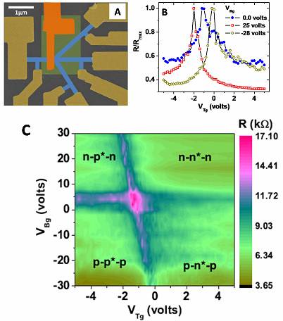
Graphene flakes were mechanically exfoliated from natural flake graphite and deposited on a Si wafer coated with 300 nm SiO2 gr_1 ; gr_3 . Single-layer flakes were identified by optical microscope and confirmed by Raman spectroscopy. Electrical leads were patterned by standard optical and e-beam lithography and the contacts were thermally evaporated (5nm Cr/ 75nm Au). Oxygen plasma (100 W for 45 sec) was used to pattern the graphene. To fabricate the top gate, 20 nm of Al2O3 was deposited as the top gate insulating layer, followed by deposition of a 200 nm wide gold electrode on top. Scanning electron microscope (SEM) image of a typical device is shown in Fig. 1A. The mobility in our samples is 2800 cmVs, which is typical for graphene on SiO2 substrates. This implies an average impurity concentration of 1010cm-2 disorder .
Electrical measurements were carried out at 4.2 K by placing the samples in vacuum in a He3 cryostat. The bias current was kept sufficiently low to avoid heating. Measurements were done in a four probe geometry with external voltage probes external_1 , using the SR 560 low noise preamplifier and PAR 124A analog lock-in amplifier equipped with an EG&G 116 preamplifier (operating in differential mode).
The resistance as a function of the back gate voltage () and the top gate voltage () is shown in Fig. 1B and 1C for a typical device, measured on the straight arm at 4.2 K. Normalized resistance as a function of is shown in Fig. 1B for three values of . For , the resistance is symmetric around the Dirac point, while for large positive and negative , it shows an asymmetry that has also been observed by others huard . Specifically, a larger resistance is found for the values of that induce carriers of the opposite polarity under the top gate, forming a p-n-p or an n-p-n junction. With a suitable combination of and , all portions of the graphene device can be p or n type, or one can make a p-n-p or an n-p-n structure, as indicated in Fig. 1C. The two crossing dark lines in Fig. 1C trace the resistance peaks corresponding to the Dirac points as a function of the top and back gate voltage, showing the regions of neutrality in the sample. The slope of the diagonal line, ( in our samples), represents the efficiency of the top gate control of the carrier density as compared to that of the back gate.
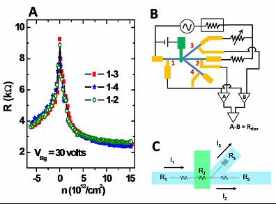
Our graphene device has four arms, one on the left side of the top gate (1) and three on the right side (2, 3 and 4). The top gate is placed over arm 1, just before the point at which arms 2, 3 and 4 branch out at different angles (arm 2 at 00, and arms 3 and 4 at 450). The resistance as a function of for = 30 volts, measured between arm 1 and each of the other three arms (in a standard four-probe configuration using non-invasive leads external_1 ) is shown in Fig. 2A. Since the three current paths share a common top-gated portion, the effect of the top gate on all three arms is almost identical. Any angle-dependent portion of this resistance would be included in the difference in the resistance as a function of of the straight arm and either of the angled arms, , or , but not in ) (arms 3 and 4 are both at 450), so the angle-dependent contribution should be identical). However, this difference would also include other angle-independent contributions (minor differences in size, geometry, or impurity configuration). As is evident in Fig. 2A, this difference is quite small, and also shows mesoscopic fluctuations that are typically observed in samples of this size savchenko .
In order to separate out the angle-dependent contribution, we use a balanced differential measurement as shown in the schematic in Fig. 2B. In each measurement, the current bias is applied between arm 1 and two of the arms on the right of the top gate, either one straight and one angled arm, or two angled arms (the schematic in Fig. 2B shows measurements that compare arms 2 and 3, while arm 4 is not connected). The resistances of the two paths are then balanced with the help of a variable resistor so that the voltage difference V between the two paths for is zero (limited by the background noise of a few nanovolts). The relevant resistances and the current branching schematic are shown in Fig. 2C. The resistance of arm 1 and the resistance of the entire p-n-p junction under the top gate are included in both current paths, and the resistances and will determine the current branching between the arms 2 and 3 at (here and are the resistances of the ballistic portions of the leads that are within the mean free path of the right p-n interface, while and are the resistances of the remaining diffusive portions of the leads). A differential measurement of the voltage drop between the two paths cancels out any common mode signal, including , and any external noise that affects both paths equally. Balancing the two arms at ensures that , with and cancelling out (being common to both paths). Applying a voltage to the top gate changes only the resistance under the top gate , which is shared by both paths and will not cause a deviation from the balanced condition - therefore, we are not measuring the resistance of the p-n-p junction, or either of the two p-n interfaces (all of which are common to both paths). A deviation from the balanced condition, , can only be caused by a redistribution of current between arms 2 and 3 as a function of the top gate. The current branching in arms 2 and 3 is determined by and , neither of which is directly affected by - any differences in geometry, size, impurity configurations and resistivity in the two arms are already cancelled out by balancing and , and neither arm is under the top gate. If, however, there were any gate-dependent difference in the transmission probability between the two arms, it would affect the distribution of current in the arms 2 and 3 within the distance from the junction of the order of the mean free path. More specifically, it would affect the current distribution through and , causing a difference in the voltage drop over and . This would cause a deviation from the balanced condition, which measures the difference in the voltage drop only over the ballistic portion (). It is this deviation from the balanced condition that we measure below. In order to relate the measurement to the transmission probability, we define a parameter with units of resistance. is then proportional to the difference in the transmission probability and reflects the current redistribution in the two leads as a function of .
For a particular back gate voltage, we begin by balancing two of the arms (2 and 3) at =0. Then, we study as a function of , shown in Fig. 3A (the balancing was done at = -28 volts and =0). shows reproducible fluctuations throughout the whole range of , which resemble mesoscopic conductance fluctuations savchenko (the amplitude of the fluctuations in units of conductance are on the order of 0.01 ). The amplitude of the fluctuations in visibly increases for positive values of , when we expect a p-n-p junction to have formed. If we balance the circuit at = 25 volts and =0, larger fluctuations in are observed below = -2 volts, when we have an n-p-n junction formed under the top gate (see Fig. 3B). In order to emphasize the amplitude of these fluctuations, we examine the derivative of as a function of (), as shown in Fig. 3C. is shown here as a function of , along with the corresponding change in resistance of the entire path to illustrate the proximity to the Dirac point. It is evident that the fluctuations are significantly larger in the p-n-p side than in the p-p-p side. Similarly, larger fluctuations are observed in the n-p-n side compared to the n-n-n side of the top gate voltage axis (Fig. 3D).
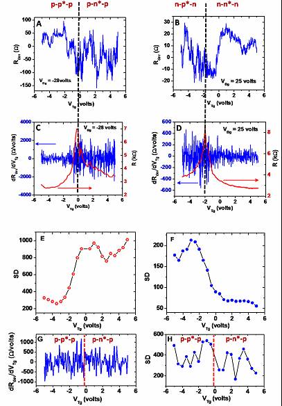
To obtain a more quantitative measure of the amplitude of these fluctuations, we divided the data points into small bins and calculated the standard deviation of as a function of . Figures 3E and 3F show the standard deviation calculated with twenty five data points per bin and averaged over four data points. It is evident that the standard deviation of the fluctuations increases by a factor of four as we cross from p-p-p to p-n-p or from n-n-n to n-p-n region (we note that the standard deviation of the fluctuations is overall larger when we have a p-n-p junction, than in the case of a n-p-n junction).
Similar results were obtained by comparing arms 2 and 4 (one straight and one angled arm). However, if we compare arms 3 and 4 (both at 450 angle with respect to the junction interface, we find that the variation in the remains nearly constant throughout the whole range of top and back gate voltages, as shown in Fig. 3G. This is also confirmed by the standard deviation shown in Fig. 3H.
There are two possible contributions to that could depend on : mesoscopic conductance fluctuations and angle-dependent transmission. The balanced differential measurement cancels out any other contributions due to the size, geometry, and other contributions that do not depend on the gate voltage. Mesoscopic conductance fluctuations are indeed expected in samples of similar size savchenko . These fluctuations are the consequence of quantum interference of electron wavefunctions scattered on impurities, and are reproducible as a function of gate voltage for a given impurity configuration. The top gate voltage in our sample does not affect the bulk of arms 2, 3 and 4, but it is likely to affect a small portion within the mean free path of the top gate. Since the top gate has a finite width, the impurity configuration along this width, while certainly similar, is not exactly identical. Therefore, would measure the difference in conductance fluctuations in small ballistic portions of two different arms. This would manifest as random, but reproducible fluctuations in as a function of , as is indeed observed in our measurement in the entire range of . In the case when a bipolar junction is formed under the top gate, the fluctuations are visibly increased. To see whether this increase reflects enhanced mesoscopic conductance fluctuations, we examine the measured by balancing different pairs of arms. Measuring all pairs of arms on three different devices, we find that increased fluctuations are observed only when the two arms are at a different angle - if we compare arms 3 and 4, the amplitude of the fluctuations remains the same throughout the whole range of . We therefore conclude that the difference in the mesoscopic conductance fluctuations in the ballistic portions of the leads is the cause of the baseline fluctuations, but cannot account for the increase in the fluctuation amplitude (leading to the four-fold increase in the standard deviation) observed when a bipolar junction has formed under the top gate.
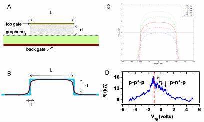
In order to examine the possibility that this increase is due to angle-dependent difference in the transmission detected on different arms of our devices, we need to consider the appropriate model for the potential barrier formed by the top gate (Fig 4A). A sharp, ballistic, rectangular barrier of length L and height d (shown in Fig. 4B in blue) would lead to perfect transmission at normal incidence and an oscillating transmission probability at other incident angles. A differential measurement of one straight and one angled arm would then result in oscillating resistance in the case of a bipolar junction, and no oscillations in the case of over-barrier transmission (p-p-p or n-n-n case). These oscillations would be superposed with the mesoscopic conductance fluctuations, resulting in increased fluctuation amplitude in the case of bipolar junction. This could, in principle, explain our results. However, given that the estimated mean free path is on the order of the top gate length, our devices are quasi-ballistic at best and it is not obvious that we can assume the potential to be sharp. Estimating the mean free path () from its relation to conductance , we find it to be around 100-200nm in our samples ( for the sample shown in Fig 2 A, evaluated at 3V). The width of the top gate in all samples is 200 nm. Therefore, we cannot assume that the entire p-n-p structure is ballistic, but we can think of it as quasi-ballistic, as some portion of carriers is likely to pass through the barrier without scattering. Alternatively, we may have to treat the p-n-p junction as two p-n junctions in series, as discussed below. A realistic barrier, however, would not have infinitely sharp edges - we expect the potential to rise over some distance (Fig. 4B). The edges can still be considered sharp if the electron wavelength is large compared to , or if . In our samples, (taking at 3V, away from the Dirac point), so we need to consider smooth edges.
Another important consideration is whether transport through each p-n junction is ballistic or diffusive. A good measure for this is a parameter , where n’ is the density gradient at zero energy, and is a parameter related to mobility through disorder . In order to observe ballistic transport through a p-n junction, it is required that . The mobility can be estimated from , where n is the carrier density and is the resistivity of the sample away from the Dirac point. The mobility in our samples is 2800 cmVs, and the top gate is placed at the height d=20nm away from graphene, as shown in Fig. 4B. The distance over which the potential increases at the p-n interface, t, can be taken to be on the order of d. Estimating the density gradient at the interface from the difference in the carrier densities on the two sides of each p-n junction over 20nm, we arrive at the value of 160, indicating that we should expect a significant ballistic contribution. This is confirmed by the calculation of the potential profiles under the top gate, shown in Fig. 4C.
A model for smooth ballistic p-n junctions was developed in reference klein_1 . This model predicts that a smooth p-n junction transmits only the carriers that approach it within a small incident angle smaller than . The transmission probability as a function of the incident angle is klein_1 : so we would expect perfect transmission for normally incident carriers, and suppressed transmission with increasing incident angle. In our samples , so we would expect efficient collimation within the mean free path away from the p-n interface. Our p-n-p (or n-p-n) junctions include two p-n interfaces - one on either edge of the top gate. The first p-n junction would then preferentially transmit more carriers that are nearly normally incident to the barrier. These carriers would arrive to the second p-n junction, which would again select more of the normally incident ones. As all the arms have the same width, and the branching point is less than away from the top-gated portion, most of the electrons coming from arm 1, that emerged in the direction normal to the second pn junction, will go straight into arm 2. The arm 3 (or 4) is placed at an angle with respect to the top gate (), so it will preferentially collect any electrons that emerged at angles close to . Here we also have to take into account the fact that the arms have a finite width, and the electrons can emerge anywhere along that width. Therefore, each arm will actually collect electrons that emerge at a small range of angles.
If we assume that the carriers tunnel through two independent p-n junctions in series, than we would expect most of the carriers to be collected by arm 2, with very few carriers going into arm 3 or 4. In this case, we would not expect to see oscillations in the transmission amplitude as a function of barrier height.
If, however, the transport through the p-n-p junction is coherent, one can expect to observe resonant tunneling through quasi-bound states due to Fabry-Perot interference klein_4 ; kim . In this case, the oscillating part of the resistance can be approximated by klein_4 ; kim :
| (1) |
where T is the transmission coefficient and is the semiclassical phase klein_4 ; kim . Taking into account nonlinear screening when evaluating T screening , this expression results in resistance oscillations with an approximate period in the carrier density of about cm-2. In our samples, this would result in oscillations with with a period of about 0.5V, which is indeed observed in four-terminal measurements of resistance on arm 2, as shown in Fig 4D. These oscillations are superimposed with the mesoscopic conductance fluctuations, as expected from Fabry-Perot resonances in the presence of disorder sds_1 . In the presence of disorder, it was found that the oscillations survive even at impurity concentrations that are by an order of magnitude larger than that observed in our samples, but become smeared by mesoscopic conductance fluctuations. Such fluctuations, in addition to inhomogeneous gate coupling due to the disorder, were also found to cause averaging over several Fabry-Perot fringes in all but the cleanest samples kim . In this picture, small-angle averaged irregular oscillations would be expected on arm 2 when a bipolar junction is formed under the top gate, with very few carriers making it to arm 3 or 4. Comparing arm 2 with either 3 or 4 would then result in the increased oscillation amplitude, while comparing arms 3 and 4 would not, as observed in our experiment.
We note that it is not necessary for the entire device to be ballistic in order to observe the angle dependence of the resistance. As long as the difference in the current distribution due to ballistic effects in a small portion of the straight and angled arms is large enough, it will manifest as the deviation from the balanced condition with changing top gate voltage. Therefore, our measurement technique specifically selects and only measures the ballistic contribution. Since all the arms share the same top-gated portion, the properties of the potential barrier are identical for straight and angled arms: there will be no differences in the pn-junction length, roughness, the nature of disorder, contact resistance and other issues that have to be taken into account when comparing different physical devices.
In conclusion, even though our measurements were limited by mesoscopic conductance fluctuations, we were able to observe angle-dependent transmission through a p-n-p junction in graphene. Using cleaner samples with higher mobility and a larger mean free path would make it possible to make more detailed angle-resolved measurements, which could lead to electron optics applications.
References
- (1) Novoselov K. S., Geim A. K., Morozov S. V., Jiang D., Zhang Y., Dubonos S. V., Grigorieva I. V., & Firsov A. A. Electric field effect in atomically thin carbon films. Science 306, 666-669 (2004).
- (2) Geim A. K., & Novoselov K. S., The rise of graphene. Nat. Mater. 6, 183-191 (2007).
- (3) Castro Neto A. H., Guinea F., Peres N. M. R., Novoselov K. S. & Geim A. K. The electronic properties of graphene. Rev. Mod. Phys. 81, 109-162 (2009).
- (4) Das Sarma S., Adam S., Hwang E. H. & Rossi E. Electronic transport in two-dimensional graphene. Rev. Mod. Phys. 83, 407-470 (2011).
- (5) Ando T., Nakanishi T., & Saito R. Berry’s Phase and Absence of Back Scattering in Carbon Nanotubes. J Phys. Soc. Jpn. 67, 2857-2862 (1998).
- (6) Suzuura H., & Ando T. Crossover from Symplectic to Orthogonal Class in a Two-Dimensional Honeycomb Lattice. Phys. Rev. Lett. 89, 266603 (2002).
- (7) Beenakker C. Andreev reflection and Klein tunneling in graphene. Rev. Mod. Phys. 80 1337-1354 (2008).
- (8) Cheianov V. V., & Fal’ko V. I. Selective transmission of Dirac electrons and ballistic magnetoresistance of n-p junctions in graphene Phys. Rev. B 74 041403 (2006).
- (9) Cheianov V. V., Fal’ko V. I., & Altshuler B. L. The Focusing of Electron Flow and a Veselago Lens in Graphene p-n Junctions. Science 315, 1252-1255 (2007).
- (10) Katsnelson M. I., Novoselov K. S., & Geim A. K. Chiral tunnelling and the Klein paradox in graphene. Nat. Phys. 2, 620-625 (2006).
- (11) Shytov A. V., Rudner M. S., & Levitov L. S. Klein Backscattering and Fabry-Perot Interference in Graphene Heterojunctions. Phys. Rev. Lett. 101, 156804 (2008).
- (12) Park C.-H., Son Y.-W., Yang L., Cohen M. L., & Louie S. G. Electron Beam Supercollimation in Graphene Superlattices. Nano. Lett. 8, 2920-2924 (2008).
- (13) Beenakker, C. W. J., Sepkhanov, R. A., Akhmerov, A. R. & Tworzydlo, J. Quantum Goos-Hänchen effect in graphene. Phys. Rev. Lett. 102, 146804 (2009).
- (14) Hartmann, R. R., Robinson, N. J. & Portnoi, M. E. Smooth electron waveguides in graphene. Phys. Rev. B 81, 245431 (2010).
- (15) Low T. & Appenzeller J. Electronic transport properties of a tilted graphene p-n junction. Phys. Rev. B 80, 155406 (2009).
- (16) Rossi E., Bardarson J. H. Brouwer P. W. & Das Sarma S. Signatures of klein tunneling in disordered graphene p-n-p junctions Phys. Rev. B 2010, 81, 121408 (2010).
- (17) Sajjad R. & Ghosh A. High efficiency switching using graphene based electron optics Appl. Phys. Lett. 99, 123101 (2011).
- (18) Huard B., Sulpizio J. A., Stander N., Todd K.,Yang B., & Goldhaber-Gordon D. Transport Measurements Across a Tunable Potential Barrier in Graphene. Phys. Rev. Lett. 98, 236803 (2007).
- (19) Stander N., Huard B., & Goldhaber-Gordon D. Evidence for Klein Tunneling in Graphene p-n Junctions.Phys. Rev. Lett. 102, 026807 (2009).
- (20) Young A. F., & Kim P. Quantum interference and Klein tunnelling in graphene heterojunctions. Nat. Phys. 5, 222-226 (2009).
- (21) Wu Y., Perebeinos V., Lin Y.-M., Low T., Xia F., & Avouris P. Quantum Behavior of Graphene Transistors near the Scaling Limit. Nano. Lett. 12, 1417-1423 (2012).
- (22) Gorbachev R. V., Mayorov A. S., Savchenko A. K., Horsell D. W., & Guinea F. Conductance of p-n-p Graphene Structures with ”Air-Bridge” Top Gates. Nano. Lett. 8, 1995-1999 (2008).
- (23) Williams J. R., Low T., Lundstrom M. S., & Marcus C. M. Gate-controlled guiding of electrons in graphene. Nat. Nano. 6, 222-225 (2011).
- (24) Sutar S., Comfort E. S., Liu J., Taniguchi T., Watanabe K., & Lee J. U. Angle-Dependent Carrier Transmission in Graphene pn Junctions. Nano. Lett. 12, 4460-4464 (2012).
- (25) Fogler M. M., Novikov D. S., Glazman L. I., & Shklovskii B. I. Effect of disorder on a graphene p-n junction. Phys. Rev. B 77, 075420 (2008).
- (26) Zhang L. M., & Fogler M. M. Nonlinear Screening and Ballistic Transport in a Graphene p-n Junction. Phys. Rev. Lett. 100, 116804 (2008).
- (27) Sonin E. B. Effect of Klein tunneling on conductance and shot noise in ballistic graphene. Phys. Rev. B 79, 195438 (2009).
- (28) Xia F., Perebeinos V., Lin Y.-M., Wu Y., & Avouris P. The origins and limits of metal-graphene junction resistance. Nat. Nano. 6, 179-184 (2011).
- (29) Giovannetti G., Khomyakov P. A., Brocks G., Karpan V. M., van den Brink J., & Kelly P. J. Doping Graphene with Metal Contacts. Phys. Rev. Lett. 101, 026803 (2008).
- (30) Lee E. J. H., Balasubramanian K., Weitz R. T., Burghard M., & Klaus Kern K. Contact and edge effects in graphene devices. Nat. Nano. 3, 486-490 (2008).
- (31) Huard B., Stander N., Sulpizio J. A., & Goldhaber-Gordon D., Evidence of the role of contacts on the observed electron-hole asymmetry in graphene. Phys. Rev. B 78, 121402(R) (2008).
- (32) Tikhonenko F. V., Horsell D. W., Gorbachev R. V.,& Savchenko A. K., Weak localization in graphene flakes. Phys. Rev. Lett. 100, 056802 (2008).