Signature of gate-tunable magnetism in graphene grafted with Pt-porphyrins
Abstract
Inducing magnetism in graphene holds great promises, such as controlling the exchange interaction with a gate electrode, and generating exotic magnetic phases. Coating graphene with magnetic molecules or atoms has so far mostly lead to decreased graphene mobility. In the present work, we show that Pt-porphyrin molecules adsorbed on graphene lead both to an enhanced mobility, and to gate-dependent magnetism. We report that porphyrins can act both as donor or acceptor molecules, depending on the initial doping of the graphene sheet. The porphyrins transfer charge and ionize around the charged impurities on graphene, and, consequently, the graphene doping is decreased and its mobility is enhanced.
In addition, ionized porphyrin molecules carry a magnetic moment. Using the sensitivity of mesoscopic transport to magnetism, in particular the superconducting proximity effect and conductance fluctuations, we explore the magnetic order induced in graphene by the interacting magnetic moments of the ionized porphyrin molecules.
Among the signatures of magnetism, we find two-terminal-magnetoresistance fluctuations with an odd component, a tell-tale sign of time reversal symmetry breaking at zero field, that does not exist in uncoated graphene samples. When graphene is connected to superconducting electrodes, the induced magnetism leads to a gate-voltage-dependent suppression of the supercurrent, modified magnetic interference patterns, and gate-voltage-dependent magnetic hysteresis. The magnetic signatures are greatest for long superconductor/graphene/superconductor junctions, and for samples with the highest initial doping, compatible with a greater number of ionized, and thus magnetic porphyrin molecules. Our findings suggest that long-range (of the order of the coherence length, or micrometers) magnetism is induced through graphene by the ionized porphyrins’ magnetic moment. This magnetic interaction is controled by the density of carriers in graphene, a tunability that could be exploited in spintronic applications.
I Introduction
Because of its conical band structure and the possibility to continuously tune the Fermi level with a gate voltage, graphene has opened a broad new field of investigation of 2D electronic transport. At low temperature the phase coherence length, of the order of one micron, offers the possibility to explore mesoscopic aspects of transport in graphene such as conductance fluctuations and proximity-induced superconductivity. More than classical transport, quantum transport is especially sensitive to the nature of scattering impurities on graphene, in particular to their charged, neutral or polar character imp . The spatial extent of the scattering potential also plays an important role: short-range neutral scatterers cause intervalley scattering, in contrast to long range charged impurities. Beyond the characterization of intrinsic impurities of graphene, it is tempting to add specific impurities to induce new functionalities and tune them in a controlled way. Adsorbates on graphene transistors have for instance been shown to affect the transport characteristics of graphene-based sensorssensors . On a more fundamental level, a longstanding goal is to induce and control physical properties involving spin degrees of freedom such as spin-orbit coupling and magnetism. Specific signatures of spin-orbit or magnetic scatterers are expected, whose effect should be tunable with the gate voltage castro08 ; Guinea12 ; Alicea ; Asmar . To reach this goal, graphene has been coated with magnetic (transition metal or rare earth) atoms LauKawakami ; Girit as well as molecular magnets, with mixed results. Adsorbed magnetic atoms reduce graphene’s mobility, with no clear concurrent magnetic signature. In contrast, the magnetisation reversal of molecular magnets has been detected in a graphene nanoconstriction Candini . Possible signatures of enhanced spin-orbit interactions have also been observed in graphene coated with small non magnetic metallic clusters Ozyilmaz . Magnetism could also be induced by creating vacancies in graphene Nair ; vacancies or adsorbing atomic hydrogen McCreary , with a doping-dependent magnetic signature. However in both cases this magnetism is induced at the cost of an unavoidable decrease of sample mobility.
In the present work, we functionalize graphene with a thin film of Pt-porphyrins. The first layer directly in contact with graphene can interact with graphene’s delocalised orbitals and is expected to form an ordered array mayne . Neutral Pt-porphyrins are non magnetic, but the ionized form carries a magnetic moment of one Bohr magneton ESR . At room temperature we find that the molecules dope the graphene, demonstrating that charge transfer occurs. Either electrons or holes can be transferred to the graphene layer, depending on its initial doping. More surprisingly, the graphene’s mobility increases upon molecules deposition. Using the high sensitivity of mesoscopic transport, in particular the superconducting proximity effect and conductance fluctuations lundberg , we show evidence of long range magnetism induced in several porphyrin-coated samples. This magnetism leads to field asymmetry of conductance fluctuations in samples with normal electrodes, and suppression of supercurrent or modified Fraunhoffer patterns in samples with superconducting electrodes. The signatures are largest for samples with high initial doping, for which more porphyrins ionize and thus become magnetic.
One implication of these findings is that it is possible to control the number of magnetic porphyrins by their degree of ionization. In all experiments this magnetism is found to depend on gate voltage, a tunability that could be exploited in spintronic devices. These findings also constitute evidence for Fermi-level controlled exchange interaction between localized spins and graphene.
II Sample preparation
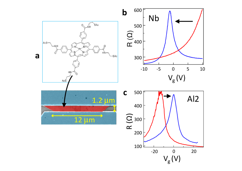
The samples are prepared by exfoliation of high quality graphite and deposition onto an oxidized doped silicon wafer (acting as a backgate). Monolayers are selected by optical microscopy. The metallic contacts are made by electron beam lithography followed by deposition of different metallic bilayers, Ti/Au, Ti/Al or Pd/Nb. All samples were measured at room temperature before deposition of the molecules. The Pt-porphyrin, see Fig.1, contains a Pt atom at the center of the characteristic cyclic organic cage of four pyrrole subunits interconnected via methine bridges (=CH). The porphyrins were prepared as described in prepaporphyrin1 . The electronic structure of porphyrins, as determined by optical absorption measurements and Scanning Tunneling Spectroscopy, is characterized by a HOMO (Highest Occupied Molecular Orbital) -LUMO (Lowest Unoccupied Molecular Orbital) gap of the order of 2 eV HomoLumo . We deposited Pt porphyrins at room temperature according to the following protocol. We first checked that deposition of the sole solvent tetrahydrofuran (THF) does not modify the gate voltage dependence of the sample’s conductance. We then deposited a 10 drop of a 1 mM solution of Pt porphyrins in THF. This corresponds to a few hundred layers of porphyrins covering the graphene after evaporation of the THF solvant. We have changed this number of layers by a factor 10 and find that the low temperature results (that demonstrate the gate-dependent magnetism) do not depend on the layer thickness, consistent with a porphyrin/graphene interaction restricted to the first layer. We have functionalised over twenty graphene samples. Among those samples, ten were investigated at low temperature both before and after functionalisation, and their characteristics are detailed in table 1.
III Charge transfer between graphene and porphyrins: Neutralization of graphene by porphyrins
At room temperature (RT), we systematically measured the gate voltage dependence of the resistance before and after porphyrin deposition. A striking neutralization effect, shown on Fig.1, was observed on all investigated samples : the Dirac point of all samples is shifted to nearly zero gate voltage after deposition. This means not only that charges are transferred between porphyrins and graphene, but also that porphyrins can be both electron donors or acceptors. Since the HOMO-LUMO gap of the porphyrin (2 eV) is much greater than the typical Fermi energy differences between the graphene samples we have investigated (0.1 eV), this implies a local pinning of the HOMO (LUMO) level of the porphyrins to the hole (electron) doped Fermi level of graphene. Electron transfer has already been reported for highly hole-doped porphyrin-grafted carbon nanotubesPrato ; Hecht , and, more recently, for highly hole-doped Zn-porphyrins-grafted grapheneapl . However, the possibility to also inject holes in graphene with porphyrins has, to our knowledge, not previously been demonstrated.
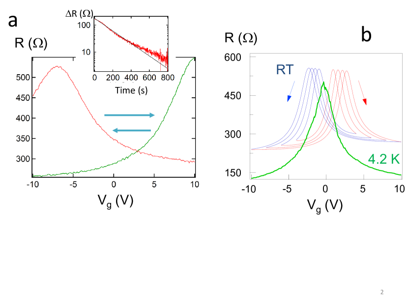
At room temperature the gate dependence of the resistance is hysteretic, with a slow exponential relaxation of the sample’s resistance in response to a fast gate voltage change. We relate the RT hysteresis and slow relaxation to hopping processes through neighboring moleculesCheccolia ; Sedghi , leading to a slow (hundred second time scale) charge transfer across porphyrin layers above the graphene. Fig.2 illustrates how the Dirac point is shifted to , with a broadened curve, after keeping the sample at a non-zero gate voltage at room temperature. This phenomenon can be seen as temporary, artificial doping of graphene by the transfer and storage of charges in the molecules. Similar effects have been observed with graphene samples functionalized with insulating nanoparticles (iron and titanium oxide, CdSe) showing evidence of charge neutralization of graphene, mobility increase and gate voltage dependent charge transfer between graphene and nanoparticles nanopart .
When cooling the sample at zero gate voltage, the Dirac point stays unchanged close to . In contrast to the RT behavior, there is no gate-dependent charge transfer at low T (below 4.2 K). This is demonstrated by magnetoresistance measurements in the quantum Hall regime, for which the carrier density , estimated with the same parameters as for the bare graphene sample (same capacitance, etc.) yields the Quantum Hall plateaus for the coated sample at exactly the same filling factors as before, see Fig. 3. Another important feature is the increase in sharpness of the curve after porphyrin deposition, with a higher resistance at the charge neutrality point (Dirac point) (see Fig.3a), implying that coating with Pt-porphyrins results in a higher sample mobility (from to near the Dirac point at 4.2 K). Hall plateaus are also better defined. These observations, along with the shift of the Dirac point to , prove that porphyrins ionize and neutralize charged impurities on graphene or on the silicon substrate, and therefore decrease the disorder scattering.
This neutralization of graphene by ionization of the porphyrins is concurrent with the formation of singly occupied impurity states close to the Dirac point (distributed between the initial and final Dirac points). Whether or not these impurity states generate a magnetic moment, corresponding to the spin of the unpaired electron delocalized over the molecule, will depend on the energy of the impurity state, as well as on graphene’s Fermi level, and thus gate voltage, as described by Uchoa et al.castro08 . In the following we present signatures of this magnetic moment and its gate-voltage dependence, detected via phase coherent transport measurements at low temperature.
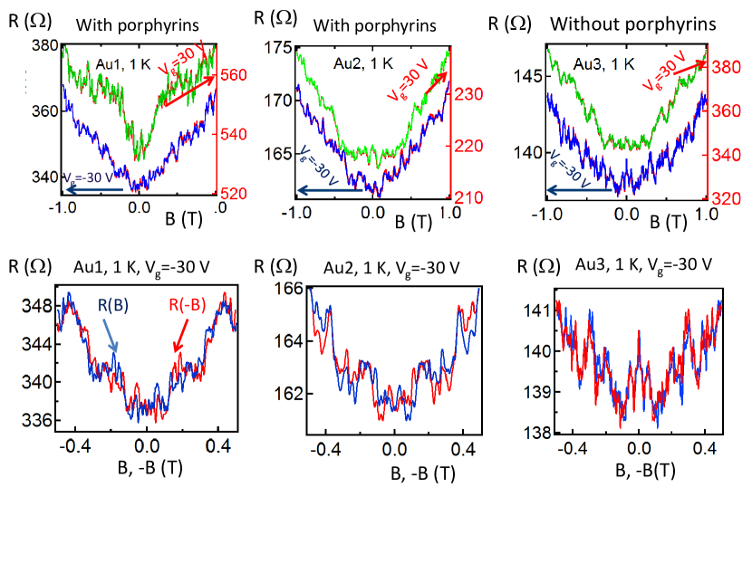
IV Signature of magnetism on samples with normal contacts
We first discuss 3 graphene samples, on the same Si substrate, with normal (non superconducting) Ti(6nm)/Au(100nm) contacts . Two of them (Au1, Au2) were coated with porphyrins, another (Au3) not. We find (see Fig. 4) that at 1 K the two-terminal resistance in perpendicular field of the uncoated sample exhibits reproducible mesoscopic magneto-resistance fluctuations due to interference between all the coherent trajectories across the samples. The amplitude of the conductance fluctuations is of the order of the conductance quantum. As for non magnetic mesoscopic samples, including graphene folk ; Ojeda2010 , the curves of the uncoated samples are even functions of magnetic field, as expected for 2 probes measurements on non magnetic mesoscopic samples that obey time reversal symmetry in zero field (see Fig.4). By contrast, the magnetoresistance of the coated samples Au1 and Au2 contains an odd component, whose amplitude is of the order of 1/3 of the even component. This indicates that time reversal symmetry is broken in those samples in zero magnetic field, a fact that we attribute to macroscopic magnetic moments perpendicular to the sample plane, extending on spatial scales comparable to the phase coherence and thermal lengths. Similar effects have been observed in mesoscopic spin glasses spinglass . This behavior must stem from frozen, long range magnetic correlations within the ionized porphyrins, whose physical origin we discuss further in the article. However, as shown in Fig.5, this asymmetry of the magnetoresistance in a perpendicular field is undetectable at very low temperature (100mK). Instead, we find a strong asymmetric and hysteretic magnetoresistance in parallel field, with a large odd component whose amplitude and sign depend on gate voltage (see supplementary materials Fig.S1). This asymmetric magnetoresistance in parallel field is not detectable at 1K. Thus, it appears that the porphyrins’ magnetic moment rotates from in-plane at 100 mK to nearly out-of-plane at 1K. Since the average distance between ionized porphyrins is a few nanometers, our findings suggest a relatively long-ranged magnetic interaction mediated by graphene’s conduction electrons or holes.
V Samples with superconducting contacts
We now turn to samples with superconducting electrodes (S/Graphene/S junctions), to exploit the sensitivity of the Josephson current to magnetism. Whereas small effects are found in short junctions of length smaller than the superconducting coherence length , (see samples Al1, Al2 and Al3 in supplementary materials), the most spectacular signatures of induced magnetism occur in long junctions for which or equivalently (with the superconducting gap, the Thouless energy and D the diffusion coefficient). This long junction regime can be achieved either with large gap electrodes such as Nb (sample Nb) or with very disordered samples with small (Ald1 and Ald2).
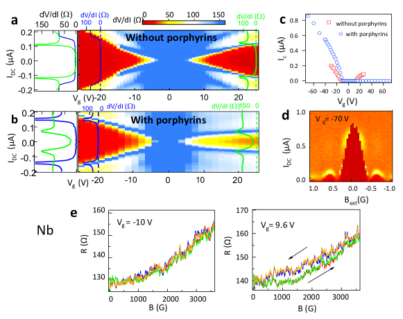
We first present a 1.2 long graphene sample connected to Pd/Nb superconducting electrodes (8nm Pd/70nm Nb, sample Nb), with 30 . Fig. 6 compares the gate voltage dependence of the differential resistance, at 100 mK, before and after porphyrins deposition. The resistance of the uncoated graphene junction is zero at low dc current, in highly doped regions (away from the Dirac point), both for hole and electron doping (Fig. 6a) Heersche ,Komatsu12 : this is the signature of a Josephson effect, a supercurrent running through the graphene because of the superconducting contacts. We previously reported that the amplitude of the maximal supercurrent, defined as the junction’s critical current, is strongly depressed in the region of the Dirac point. We attribute that effect, observed only in long junctions, to specular reflections of the Andreev pairs on very low carrier density regions (puddles) where the local Fermi energy is smaller than the proximity induced superconducting gap (see Komatsu12 for a detailed discussion of these findings). It is clear that at high doping () the supercurrent exists for both electron and hole doping, as also shown in fig 6c. In stark contrast to this bipolar Josephson effect through pristine graphene (Fig. 6a and 6c), we find that after deposition of the porphyrins, the Josephson current is enhanced in the hole doped region but suppressed in the electron-doped region. Only a dip in the differential resistance is visible at low current and high positive gate voltage, but no strictly zero resistance and no supercurrent(Fig. 6b). Fig. 6c, which displays the critical current amplitude as a function of gate voltage, shows this strong asymmetry of the gate voltage dependence of the supercurrent after deposition of the porphyrins. The absence of supercurrent in the electron doped region was checked for gate voltages up to 60V.
We attribute this extinction of the critical current, at high positive gate voltage only, to an inhomogeneous magnetic field on graphene created by the staggered magnetism of the porphyrins. This destroys the constructive interferences between the Andreev pairs that carry the Josephson current. This sensitivity of the critical current to small magnetic perturbations is illustrated by the field dependence of the supercurrent in this junction, and its narrow Fraunhoffer interference Fraunhoffer pattern (Fig.6d). It is clear that a field as small as a fraction of a Gauss can suppress the induced supercurrent through graphene, because of destructive interference between Andreev pairs diffusing across the graphene Chiodi . This explains how the porphyrin’s magnetic spins, if they lead to correlated magnetic regions at positive gate voltage, can create an inhomogeneous magnetic flux sufficient to destroy the proximity effect, thereby leading to the observed unipolar supercurrent.
Another indication of gate-voltage -dependent magnetism comes from the magnetoresistance in a perpendicular magnetic field, (Fig. 6e), which is a hysteretic function of field at , whereas there is no hysteresis for . This absence of magnetic hysteresis and the large Josephson current in the hole doped region consistently indicate either a quenched magnetic moment for the porphyrins or a reduced exchange interaction between porphyrin’s localised spins and the graphene holes. Moreover the magnetic hysteresis in the electron doped region () points to the formation of a magnetic order of the molecular spins, with partially oriented magnetic domains, generating a non uniform magnetic field that is revealed by the magnetoresistance of graphene, and explains the suppressed Josephson current for this doping. No such effect is visible at high hole doping, which we attribute to the absence of magnetism in this gate voltage range. The asymmetry of induced magnetism with respect to the sign of gate voltage is striking. It was not observed in samples Au1 and Au2 discussed in the previous section but exists in samples with TiAl contacts discussed in the next section. This gate voltage “polarity” is probably strongly dependent on the initial doping and mobility of the graphene before deposition of porphyrins, (see discussion below).
The signatures of magnetism are even more striking in data obtained on two last samples, Ald1 and Ald2, with Ti/Al contacts. These samples were initially highly electron-doped (Dirac point below , see inset of Fig. 7), as the result of oxygen plasma cleaning of the substrate before graphene deposition. Coating with porphyrins resulted in a shift of graphene’s Dirac point to nearly zero gate voltage, despite the strong initial doping. This spectacular observation attests the huge capacity of charge transfer and neutralization of porphyrins. In this case, the porphyrins must act as acceptors of electrons to neutralize these initially electron-doped graphene samples. We expect a much higher concentration of ionized porphyrins in these samples compared to the ones discussed above, where the Dirac point shift did not exceed 15 V. The high resistance at the Dirac point, (40 ), indicates a mobility at least 10 times smaller than the samples discussed previously. As a result we estimate a Thouless energy of the order of , much smaller than the superconducting contacts gap of the order of . The samples are thus also in the long junction limit. We do not observe a supercurrent, at any gate voltage, but see up to a drop of differential resistance at zero bias at high electron or hole doping. The low field magnetoresistance of sample Ald1 for different gate voltages is shown in Fig.7 . Whereas at high doping the magnetoresistance dips at zero field and displays oscillations typical of a Fraunhofer interference pattern, the magnetoresistance is clearly peaked at close to the Dirac point, and displays jumps at specific magnetic fields. Field asymmetry and hysteresis are observed for all gate voltages, indicating that this magnetoresistance is due to correlated magnetic regions in the graphene sample. This magnetism is however asymmetric with respect to the Dirac point. It is maximum for negative gate voltage and decreases for positive gate voltage. This is illustrated in the inset of Fig.7 showing the variance of the odd component of the magnetoresistance renormalized to the average total resistance as a function of the gate voltage. We attribute this asymmetry (opposite to Nb sample case) to the initial strong electron doping of the samples.
We have conducted similar investigations in short junction samples (see supplementary materials). Whereas porphyrins coating does not suppress the critical current at zero field, we do find distortions of the Fraunhofer patterns, as well as important asymmetries with respect to the electron/hole doping in finite magnetic field (at the edges of the Fraunhofer lobes).
VI Discussion
We attribute the doping-dependent asymmetries, hysteresis in magnetic field, and doping-dependent suppression of Josephson current, to a gate-voltage dependent magnetism due to the ionized porphyrin molecules. Moreover these results imply the existence of magnetic domains in the samples, and therefore interactions between the individual magnetic moments of the porphyrins. In addition, the data is consistent with magnetic moments preferentially aligned, at very low T, in the molecules’ plane, parallel to the graphene layer. This is evidenced by the strong hysteretic odd component of the in-plane magnetoresistance at low temperature in the graphene samples connected to normal electrodes (see supplementary materials). By contrast, when graphene is connected to superconducting electrodes, the hysteresis occurs also for perpendicular field. We explain this by the focusing and bending of the field lines by the superconducting electrodes, so that a perpendicular external field leads to a local field on the graphene sheet that contains both parallel and perpendicular components. Finally, we have also checked that there is no magnetic hysteresis or asymmetry both with normal or superconducting electrodes in the absence of porphyrins (see supplementary materials).
The physics of magnetic impurities on graphene has led to a variety of interesting theoretical predictions specific to the band structure of graphene. Unlike metals, the exchange coupling in graphene is expected to be controlled by gating Guinea12 . This effect has two important consequences. First, the amplitude of the magnetic moment of an individual impurity should strongly depend on gate voltage, causing a tunable Kondo effect. Depending on the relative energy of the impurity level with respect to the Dirac point, its magnetic state could be highly asymmetric with gate voltage castro08 with impurities which have a non zero magnetic moment for only one sign of gate voltage. Second, the long range magnetic Rudderman, Kittel, Kasuya,Yosida (RKKY) interactions mediated by the carriers should also be gate voltage dependent. Such interactions have been investigated theoretically and numerically by several groupsGuinea12 ; RKKY . Characteristic coupling energies in the Kelvin range are predicted between spins 1/2 a few nanometers apart. The magnetic hysteresis we observe could then be explained by a spin glass type of order taking place at low temperature.
Interestingly, it was recently shown yao2014 that exchange interactions in proximity induced superconducting graphene are enhanced on the scale of the coherence length compared to the normal state and acquire an antiferromagnetic sign in the vicinity of the Dirac point. Our results show that porphyrins coated graphene offers the possibility to explore this physics as well. Of course extrapolating these theoretical findings on the exchange coupling between localized spins on graphene to the case of Pt-porphyrins, where each spin is localized over the entire nanometer sized molecule is still a challenge Nickel .
At this stage, let us summarize our understanding of the non-systematic occurrence of the gate-voltage polarity in the magnetism we report. The gate-voltage polarity of magnetism is explained by the initial doping of graphene before porphyrins deposition, and the subsequent pinning of the HOMO or LUMO level of the Porphyrins upon coating and charge transfer. This leads to impurity states on average below the Dirac point for initially electron doped graphene (Nb sample), and above the Dirac point for initially hole-doped graphene (sample Ald1 and Ald2). As shown in castro08 , there is a limited gate range over which these impurity states are singly occupied and thus magnetic, and the range differs for both cases. The range nonetheless extends around the impurity levels energies, explaining why the magnetism should be more pronounced in positive gate voltage in the Nb sample, and negative gate voltage for the Ald1 and Ald2 samples. In contrast, samples with initially relatively broad Dirac peaks centered close to zero gate voltage due to both electron and hole pockets (such as Au1 and Au2 samples), are bound to have impurity levels both above and below the Dirac point, in a relatively wide range, and consequently magnetism is expected for both positive and negative gate voltage.
In conclusion, this gate voltage-dependent long-range order of magnetic porphyrins mediated by graphene’s carriers is of great potential interest and motivates further investigations of different porphyrin species, including metal free porphyrins or ones with a magnetic atom such as Fe or Co. Our findings show that it is possible to control the number of magnetic porphyrins by their degree of ionisation. This suggests interesting possibilities such as controling the magnetism by a gate voltage quench of graphene, or with a controlled concentration of charged defects. Finally we provide a new route for inducing gate-dependent long-range magnetism in graphene without destroying the sample mobility.
VII Acknowledgements
We acknowledge ANR Supergraph and CNRS for funding, Juan Manuel Aguilar, Alexei Chepelianskii, Richard Deblock, Andrew Mayne, Claude Pasquier, Laurent Simon and Alberto Zobelli for helpful discussions, and M. Feigelmann for suggesting that the suppressed proximity effect could be due to the molecules’ magnetism.
References
- (1) A. H. Castro Neto, F. Guinea, N. M. R. Peres, K. S. Novoselov, and A. K. Geim, “The electronic properties of graphene”, Rev. Mod. Phys. 81, 109. M. Monteverde, C. Ojeda-Aristizabal, R. Weil, K. Bennaceur, M. Ferrier, S. Guéron, C. Glattli, H. Bouchiat, J. N. Fuchs, and D. L. Maslov, “ Transport and Elastic Scattering Times as Probes of the Nature of Impurity Scattering in Single-Layer and Bilayer Graphene”, Phys. Rev. Lett.104, 126801 (2010).
- (2) Schedin, F.; Geim, A. K. Morozov, S. V. Hill,E. W.; Blake, P. Katsnelson, Novoselov, K. S., “ Detection of individual gas molecules adsorbed on graphene”, Nat. Mater. 6 (9), 652 (2007).
- (3) Kotov V. N., Uchoa B., Pereira V. M. , Guinea F. , Castro Neto A.H., “ Electron-electron interactions in graphene: current status and perspectives”, Rev. Mod. Phys. 84, 1067-1124 (2012).
- (4) Weeks, C., Hu, J., Alicea, J., Franz, M., and Wu, R., “Engineering a Robust Quantum Spin Hall State in Graphene via Adatom Deposition”, Phys. Rev. X 1, 021001 (2011).
- (5) Asmar, Mahmoud M., Ulloa, Sergio E., ” Spin-Orbit Interaction and Isotropic Electronic Transport in Graphene”, Phys. Rev. Lett. 112, 136602 (2014).
- (6) Bruno Uchoa, Valeri N. Kotov, N. M. R. Peres, and A. H. Castro Neto, “Localized Magnetic States in Graphene”, Phys. Rev. Lett. 101, 026805 (2008).
- (7) Pi K. et al.,” Electronic doping and scattering by transition metals on graphene”, Phys. Rev. B. 80, 075406 (2009).
- (8) Alemani M. et al. , “Effect of gadolinium adatoms on the transport properties of graphene”, Phys. Rev. B 86, 075433 (2012).
- (9) Jayakumar Balakrishnan, Gavin Kok Wai Koon, Ahmet Avsar, Yuda Ho, Jong Hak Lee, Manu Jaiswal, Seung-Jae Baeck, Jong-Hyun Ahn, Aires Ferreira, Miguel A. Cazalilla, Antonio H. Castro Neto and Barbaros Ozyilmaz:, ”Giant Spin Hall Effect in Graphene Grown by Chemical Vapor Deposition”,Nature Communications 5, 4748 (2014).
- (10) M. B. Lundeberg, R. Yang, J. Renard, and J. A. Folk, Defect-Mediated Spin Relaxation and Dephasing in Graphene, Phys. Rev. Lett. 110, 156601 (2013).
- (11) R. R. Nair, M. Sepioni, I-Ling Tsai, O. Lehtinen, J. Keinonen, A. V. Krasheninnikov, T. Thomson, A. K. Geim and I. V. Grigorieva, “Spin-half paramagnetism in graphene induced by point defects”, Nature Physics 8, 199-202 (2012).
- (12) A. Candini, C. Alvino, W. Wernsdorfer, and M. Affronte, “Hysteresis loops of magnetoconductance in graphene devices”, Phys. Rev. B 83, 121401(R) (2011).
- (13) Kathleen M. McCreary, Adrian G. Swartz, Wei Han, Jaroslav Fabian and Roland K. Kawakami, “Magnetic Moment Formation in Graphene Detected by Scattering of Pure Spin Currents”, Phys. Rev. Lett. 109, 186604 (2012).
- (14) Candini A., Klyatskaya S., Ruben M., Wernsdorfer W., and Affronte M., “Graphene spintronic devices with molecular nanomagnets”, Nano Lett., 11 (7), 2634 (2011).
- (15) Mayne A. et al., to be published.
- (16) Chen P., Finikova O. S. , Ou A., Vinogradov S. A. , and Kadish K. M., “ Electrochemistry of platinum(II) porphyrins: effect of substituents and -extension on redox potentials and site of electron transfer”, Inorg. Chem. 51, 6200 (2012).
- (17) G. Clavé, G. Delport, C. Roquelet, J.-S. Lauret, E. Deleporte, F. Vialla, B. Langlois, R. Parret, C. Voisin, P. Roussignol, B. Jousselme, A. Gloter, O. Stephan, A. Filoramo, V. Derycke and S. Campidelli, “Functionalization of Carbon Nanotubes through Polymerization in Micelles: A Bridge between the Covalent and Noncovalent Methods”, Chem. Mater., 25, 2700-2707 (2013): PtII tetrakis (4-carboxyphenyl)-porphyrin (15 mg, 10.8 mol) was dissolved in NMP (4 ml). S-acetylcysteamine hydrochloride (13.54 mg, 86 mol), benzotriazol-1-yl-oxytripyrrolidinophosphonium hexafluorophosphate (PyBOP) reagent (44.7 mg, 86 mol) and dry DIEA (30 l, 172 mol) were sequentially added and the resulting reaction mixture was stirred at room temperature for 4 h. The reaction was checked for completion by TLC (/MeOH, 96:4, v/v). Thereafter, the crude was diluted with AcOEt (40 ml), washed by aq. 10 citric acid (40 ml), aq. sat. (40 ml) and brine (40 ml). The organic layer was dried over , filtrated and evaporated to dryness. The resulting residue was purified by chromatography on a silica gel, eluent (/MeOH: 100/0 to 97/3), yielding porphyrins as a brown-orange solid (9.9 mg, 7.1 mol, yield = 66 ). NMR (300 MHz, ): = 3.64 (s, 3H), 3.85 (t, J = 5.1 Hz, 2H), 4.16-4.19, (m, 2H), 8.09 (s, 8H), 8.15-8.23 (m, 12H), 8.70 (s, 4H). MS (MALDI-TOF) m/z = 1387.26 [M]+, calculated for Pt: 1387.28 g/mol.
- (18) Scudiero L., Barlow Dan E., Mazur Ursula, and Hipps, “K. W. Scanning Tunneling Microscopy, Orbital-Mediated Tunneling Spectroscopy, and Ultraviolet Photoelectron Spectroscopy of Metal(II) Tetraphenylporphyrins Deposited from Vapor”, J. Am. Chem. Soc. 123, 4073 2001.
- (19) Tasis D., Tagmatarchis N., Bianco N., and Prato M., “Chemistry of carbon nanotubes”, Chem. Rev. 106, 1105 (2006).
- (20) Hecht D.S. et al. , “Bioinspired Detection of Light Using a Porphyrin-Sensitized Single-Wall Nanotube Field Effect Transistor”, Nano Lett. 6, 2031-2036 (2006).
- (21) P. Checcolia P. et al., “Tetra-phenyl porphyrin based thin film transistors”, Synth. Metals 138, 261-266 (2003).
- (22) Sedghi G. et al. , “Long-range electron tunnelling in oligoporphyrin molecular wires”, Nature Nanotechnology 6, 517-523 (2011).
- (23) Choi M. S. et al., “Gate-dependent photoconductivity of single layer graphene grafted with metalloporphyrin molecules”, Appl. Phys. Lett. 100, 163116 (2012).
- (24) Mark B. Lundeberg and Joshua A. Folk, Spin-resolved quantum interference in graphene Nature Physics 5, 894 (2009)
- (25) Deqi Wang, Xinfei Liu, Le He, Yadong Yin, Di Wu and Jing Shi, Manipulating Graphene Mobility and Charge Neutral Point with Ligand-Bound Nanoparticles as Charge Reservoir Nano Lett. 10, 4989 (2010).
- (26) C. Ojeda-Aristizabal, M. Monteverde, R. Weil, M. Ferrier, S. Guéron, and H. Bouchiat, “ Conductance Fluctuations and Field Asymmetry of Rectification in Graphene”, Phys. Rev. Lett. 104, 186802 (2010).
- (27) P. G. N. de Vegvar, L. P. Levy, and T. A. Fulton, “ Conductance Fluctuations of Mesoscopic Spin Glasses”, Phys. Rev. Lett. 66, 2380 (1991).
- (28) All reported experiments with supercurrents induced through graphene found a bipolar proximity effect. The first report is Heersche Hubert B., Jarillo-Herrero P., Oostinga Jeroen B., Vandersypen Lieven M. K. and Morpurgo Alberto F., “Bipolar supercurrent in graphene”, Nature 446, 56-59 (2007). Other references are given in Komatsu12 .
- (29) Komatsu K., Li C., Autier-Laurent S., Bouchiat H. , and Guéron S., “Superconducting proximity effect in long superconductor/graphene/superconductor junctions: From specular Andreev reflection at zero field to the quantum Hall regime”, Phys. Rev. B 88, 115412 (2012).
- (30) A flux quantum through the area of the sample ( corresponds to a field of 3 Gauss, which is much larger than the value of 0.4 Gauss measured experimentally. We understand this effect (also reported in many other papers on the proximity effect in 2D materials) as due to the focusing of field lines between the 2 massive Nb superconducting electrodes whose width is equal to 5 microns.
- (31) Chiodi F. et al. , “Geometry-related magnetic interference patterns in long SNS Josephson junctions”, Phys. Rev. B 86, 064510 (2012).
- (32) Black-Schaffer A. M., “ RKKY coupling in graphene”, Phys. Rev. B 81, 205416 (2010).
- (33) N. Y. Yao,1 L. I. Glazman, E. A. Demler,1 M. D. Lukin, and J. D. Sau, “Enhanced anti-ferromagnetic exchange between magnetic impurities in a superconducting host”, Phys. Rev. Lett. 113, 087202 (2014).
- (34) Christian F. Hermanns, Kartick Tarafder, Matthias Bernien, Alex Krüger, Yin-Ming Chang, Peter M. Oppeneer, and Wolfgang Kuch, Advanced Materials 25, 3473 (2013).


| Sample | Contact | Length () | width () | ||
| Ti/Au | 0.8 | 3.5 | 2000 | -10 | |
| Ti/Au | 0.7 | 8 | 1400 | ||
| Ti/Au | 0.8 | 3.5 | 1600 | no porph. | |
| Pd/Nb | 1.2 | 12 | 5000 | -10 | |
| Ti/Al | 0.5 | 3.4 | 3000 | no porph. | |
| Ti/Al | 0.45 | 4 | 2000 | 15 | |
| Ti/Al | 0.5 | 4 | 2000 | 15 | |
| Ti/Al | 0.4 | 2.6 | 150 | ||
| Ti/Al | 0.6 | 4 |