Theoretical Model of Superconducting Spintronic SIsFS Devices
Abstract
Motivated by recent progress in development of cryogenic memory compatible with single flux quantum (SFQ) circuits we have performed a theoretical study of magnetic SIsFS Josephson junctions, where ’S’ is a bulk superconductor, ’s’ is a thin superconducting film, ’F’ is a metallic ferromagnet and ’I’ is an insulator. We calculate the Josephson current as a function of s and F layers thickness, temperature and exchange energy of F film. We outline several modes of operation of these junctions and demonstrate their unique ability to have large product of a critical current and a normal-state resistance in the state, comparable to that in SIS tunnel junctions commonly used in SFQ circuits. We develop a model describing switching of the Josephson critical current in these devices by external magnetic field. The results are in good agreement with the experimental data for Nb-Al/AlOx-Nb-Pd0.99Fe0.01-Nb junctions.
pacs:
74.45.+c, 74.50.+r, 74.78.Fk, 85.25.CpPractical applications of superconducting digital circuits were significantly limited by the relatively low capacity of superconducting memory. This motivated initial proposals to use superconductor/ferromagnet (S/F) hybrid structures as basis for the development in cryogenic magnetic Random Access Memories (RAMs) Oh ; Tagirov ; Held . Following the first experimental realization of SFS Josephson junctions RyazanovU ; Ryazanov , much attention was paid to realize Josephson devices with complex magnetic barriers allowing switching between high and low critical currents. A number of different device structures were considered VolkovAF ; GKF1 ; VolkovAF2 ; Houzet ; Karminskaya1 ; Karminskaya2 ; Gabor ; BirgeLR ; Bolginov based either on superconducting spintronics effects or singlet-triplet switching within the magnetic barrier. However, these approaches were based on structures with reduced characteristic voltage of junctions.
Recently, successful realization of switchable Nb-Al/AlOx-Nb-Pd0.99Fe0.01-Nb junctions was reported in Larkin ; Vernik ; Ryazanov3 . These junctions are of SIsFS type, i.e., a serial connection of the SIs tunnel junction and sFS sandwich. SIsFS structure has high characteristic voltage, due to the presence of tunnel barrier ’I’. At the same time the whole structure behaves as a single junction with respect to an external magnetic field and magnetic flux penetrating into the structure, since the intermediate layer s is too thin to screen magnetic field. As a result, the magnetic field entering the Pd0.99Fe0.01 layer will modify its effective magnetization, facilitating the critical current control of the whole double-barrier SIsFS structure. According to Ref. Uspenskaya , effective magnetization in the dilute Pd0.99Fe0.01 is controlled by Fe-rich Pd3Fe nanoclusters, which can be easily reordered by a weak magnetic field.
The purpose of this paper is to develop a theory describing various modes of operation of SIsFS Josephson devices. We propose a quasiclassical model for a double-barrier Josephson structure in which magnetic and spin states of the F-film in an sFS part of the structure can change the properties and even the ground state of its Sis part. As a result, an external magnetic field may switch the junction from a superconducting to a resistive state or may transform a conventional current-phase relation to an inverted one. We compare the results with experimental data recently obtained for for Nb-Al/AlOx-Nb-Pd0.99Fe0.01-Nb junctions.
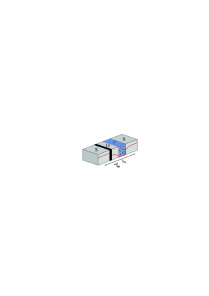
We consider the multilayered structure presented in Fig.1. It consists of two superconducting electrodes ’S’ separated by a tunnel barrier ’I’, an intermediate thin superconducting film ’s’ and a ferromagnetic layer ’F’. To describe the supercurrent transport in the structure, we assume that the conditions of a dirty limit are fulfilled for all metals. We also assume that all superconducting films in the structure are made from identical materials, i.e., they can be described by the same critical temperature, and coherence length, , where is the electronic diffusion coefficient. The tunnel barrier I and the sF and FS interfaces are characterized, respectively, by the following parameters and Here and are the area and the resistances of the interfaces, and are the coherence lengths and normal state resistivities of S and F materials, respectively. Under the above conditions the Josephson effect in the SIsFS junctions can be described by solving the Usadel equations Usadel ; RevG ; RevB ; RevV with Kupriyanov-Lukichev (KL) boundary conditions KL at Is, sF and FS interfaces and with the bulk pair potential in the depth of S-electrodes.
The formulated above boundary problem has been solved numerically. The results are summarized in Figs.2-4, where various modes of operation of the structure are defined according to chosen materials and layer thicknesses. These modes are clearly defined by the dependencies of characteristic voltage on thickness of intermediate superconductor, and ferromagnetic, layers (see Fig.2 - Fig.4).
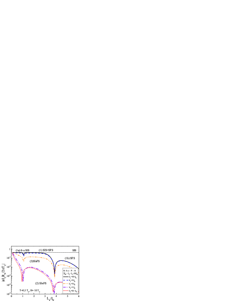
Mode (1) in Fig.2. If the thickness of the middle s-electrode, , is much larger than the critical thickness of s layer, which separates the different modes of operation in SIsFS structures, the pair potential in the s layer is close to that of bulk material. Note that the critical thickness in an sN (sF) bilayer at a given temperature is generally defined as a minimal thickness of an s-layer when superconductivity still exists. In the mode (1) the structure can be considered as a pair of SIs and sFS junctions connected in series. Therefore, the properties of the structure in parameter range (1) are almost independent on the thickness and are determined by the junction with smallest critical current. It is seen from Fig.2 that for the given parameter set, the critical thickness of the s layer, is close to
Mode (1a) in Fig.2. In the ordinary case of , the behavior of the structure coincides with that of conventional SIS junction with one important distinction - the sFS junction can turn the SIsFS structure into a -state. At the same time, other properties like high product and sinusoidal current-phase relation are preserved in the -state. Therefore the structure can be called switchable - SIS junction.
Mode (1b) in Fig.2. Another limiting case is realized for large values and high exchange fields . Namely, the structure transforms into a standard SFS-junction without any influence of tunnel barrier.
Mode (2) in Fig.2. The absence of superconductivity in the s-electrode in the opposite case () leads to formation of the complex -InF- weak link area, where n marks the intermediate s film in the normal state. It results in much smaller critical current value , with the magnitude close to that in well-known SIFS junctions Vasenko . The dependence of on the thickness is weak due to large decay length in the n-region with suppressed superconductivity.
Mode (3) in Fig.2. Conversely, in the intermediate case () the properties of the structure are extra sensitive to variations of the decay lengths parameters. Within the considered intermediate thickness range the system may transform from the mode (1) to the mode (2). Moreover, in this situation the system is sensitive to the F-layer parameters (thickness and exchange field ), since these parameters control the suppression of superconductivity in the sF bilayer.
This sensitivity allows one to change an operation mode by changing the parameters such as effective exchange field and temperature Note, that depending on the domain structure of a ferromagnet and morphology of the F-film it might be possible to control the effective exchange field .
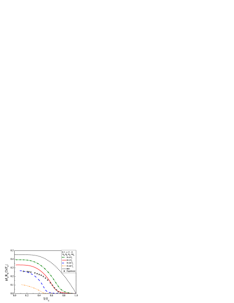
Fig.3 demonstrates the temperature dependence of the critical current in the structures with thickness around critical one ( ) for different values of exchange field . These structures are characterized by the existence of the effective critical temperature which corresponds to the appearance of superconductivity in middle s-layer and, correspondingly, to an exponential growth of the current. Therefore, may significantly shift during remagnetization of the system (due to changing of H, as pointed out above). Thus, system can exist either in the superconducting or in the normal state depending on the history of the application of a magnetic field. On the other hand, from point of view of practical applications, the - SIS mode (1a) seems more relevant.
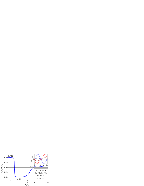
Fig.4 demonstrates that change of F-layer thickness leads to 0- transition. The system can be switched into a -state keeping the value of product, i.e., Josephson frequency, on the level characteristic for tunnel SIS junctions. Moreover, it should be noted that this property of the considered structure is unique. In the conventional SFS devices in order to reach the -state it is necessary to realize either or very large values of the parameter at the SF interfaces. In both cases the product in the -state is strongly reduced RevG ; RevB ; RevV ; Vasenko .
External magnetic field. In the parameter range when SIsFS junction is in (1a) mode and far from the transition, current-phase relation has a sinusoidal form, . To calculate the dependence of from external magnetic field, , we may use the standard Fraunhofer expression,
| (1) |
where
| (2) |
is magnetic flux inside of SIsFS junction, is flux quantum, , is London penetration depth of S electrodes, is thickness of I layer, is the full number of clusters, are the concentrations of clusters in the F layer oriented parallel () or antiparallel () to the direction of in the saturation region and is an average magnetic field generated by a single magnetic cluster. In our simple model, is assumed to be a constant, while and are functions of . We assume further that the probability density of a flip of a cluster in is described by a Gaussian distribution
| (3) |
where is the value of magnetic field, at which the flip of a cluster takes place. The expectation, and the standard deviation, in (3) are independent on values. These parameters, as well as product (i.e. saturation of the magnetization magnitude) in Eq.(2) can be found by fitting the magnetization curve
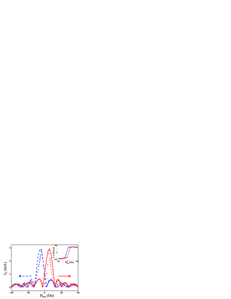
We apply this model to explain the data experimentally observed in Ref.Vernik in SIsFS structures having cross-section area m2 and F layer thickness nm. Figure 5 demonstrates the experimental dependencies of critical current versus increasing (open circles) and decreasing (open squares) external magnetic field . Solid and dashed lines present the microscopic fitting of the data. From hysteretic dependencies of F layer magnetization shown in insert in Fig. 5 we get Oe, Oe and product G. Remaining fitting parameters can be set from the current magnitude in the main maximum mA and from the difference between zeros of dependence in the saturation region, where oscillation period depends entirely on the effective length of structure nm.
The initial strong magnetic field remagnetize all clusters of F layer into the homogeneous state . Gradual growth of the external field provides the conventional Fraunhofer pattern (solid line) with expected maximum at the positive value corresponding to zero flux . However, the clusters start to flip around the point . As a result, the period of Fraunhofer oscillations decreases. Similar situation takes place during field sweeping in the opposite direction (dashed line), from large positive to negative values. The densities and can be described by the expression, for forward and backward remagnitizations, respectively. Here is the error function.
In this paper we have demonstrated a number of unique properties of SIsFS Josephson junctions. These structures exhibit a large product in the state comparable to that in SIS tunnel junctions commonly used in SFQ devices. Moreover, the whole structure behaves as a single junction with respect to an external magnetic field . Based on that, we have developed simple model describing the behavior of the critical current in these junctions in external field taking into account remagnetization of the F-layer. The model explains asymmetric Fraunhofer oscillations in Nb-Al/AlOx-Nb-Pd0.99Fe0.01-Nb junctions reported in Larkin ; Vernik ; Ryazanov3 . These effects provide the possibility to realize magnetic memory compatible with energy-efficient SFQ digital circuits Mukhanov1 with high switching speed.
This work was supported by the Russian Foundation for Basic Research, Russian Ministry of Education and Science, Dynasty Foundation, Scholarship of the President of the Russian Federation and Dutch FOM.
References
- (1) S. Oh, D. Youm, and M. Beasley, Appl. Phys. Lett. 71, 2376 (1997).
- (2) L. R. Tagirov, Phys. Rev. Lett. 83, 2058 (1999).
- (3) R. Held, J. Xu, A. Schmehl, C.W. Schneider, J. Mannhart, and M. Beasley, Appl. Phys. Lett. 89, 163509 (2006).
- (4) V.V. Ryazanov, Physics - Uspekhi 42, 825 (1999).
- (5) V.V. Ryazanov, V.A. Oboznov, A.Yu. Rusanov, A.V. Veretennikov, A.A. Golubov, J. Aarts, Phys. Rev. Lett. 86, 2427 (2001).
- (6) F. S. Bergeret, A. F. Volkov, and K. B. Efetov, Phys. Rev. Lett. 86, 3140 (2001).
- (7) A. A. Golubov, M. Yu. Kupriyanov, and Ya. V. Fominov, Pis’ma v ZhETF 75, 223 (2002) [JETP Letters 75, 190 (2002)].
- (8) A. F. Volkov, F. S. Bergeret, and K. B. Efetov, Phys. Rev. B 64, 134506 (2001).
- (9) M. Houzet and A. I. Buzdin, Phys. Rev. B 76, 060504(R) (2007).
- (10) T. Yu. Karminskaya and M. Yu. Kupriyanov, Pis’ma v ZhETF 85, 343 (2007) [JETP Lett. 85, 286 (2007)].
- (11) T. Yu. Karminskaya, M. Yu. Kupriyanov, and A. A. Golubov, Pis’ma v ZhETF 87, 657 (2008) [JETP Lett. 87, 570 (2008)].
- (12) G. B. Halasz, M. G. Blamire, and J. W. A. Robinson, Phys. Rev. B 84, 024517 (2011).
- (13) T. S. Khaire, M. A. Khasawneh, W. P. Pratt, Jr., and N. O. Birge, Phys. Rev. Lett. 104, 137002 (2010).
- (14) V. V. Bol’ginov, V. S. Stolyarov, D. S. Sobanin, A. L. Karpovich, and V. V. Ryazanov, Pis’ma v ZhETF 95, 408 (2012) [JETP Lett. 95, 366 (2012)].
- (15) T. I. Larkin, V. V. Bol’ginov, V. S. Stolyarov, V. V. Ryazanov, I. V. Vernik, S. K. Tolpygo, and O. A. Mukhanov, Appl. Phys. Lett. 100, 222601 (2012).
- (16) I. V. Vernik, V. V. Bol’ginov, S. V. Bakurskiy, A. A.Golubov, M. Y. Kupriyanov, V. V. Ryazanov, O. A. Mukhanov, IEEE Trans. Appl. Supercond. 23, 1701208 (2013).
- (17) V. V. Ryazanov, V. V. Bol’ginov, D. S. Sobanin, I. V. Vernik, S. K. Tolpygo, A. M. Kadin, O. A. Mukhanov, Physics Procedia 36, 35 (2012).
- (18) L. S. Uspenskay, A. L. Rahmanov, L. A. Dorosinskiy, A. A. Chugunov, V. S. Stolyarov, O. V. Skryabina, and S. V. Egorov, Pis ma v ZhETF 97, 176 (2013) [JETP Lett. 97, 155 (2013)].
- (19) K. D. Usadel, Phys. Rev. Lett. 25, 507 (1970).
- (20) A. A. Golubov, M. Yu. Kupriyanov, E. Il’ichev, Rev. Mod. Phys. 76, 411 (2004).
- (21) A. I. Buzdin, Rev. Mod. Phys. 77, 935 (2005).
- (22) F. S. Bergeret, A. F. Volkov, K. B. Efetov, Rev. Mod. Phys. 77, 1321 (2005).
- (23) M. Yu. Kuprianov and V. F. Lukichev, Zh. Eksp. Teor. Fiz. 94, 139 (1988) [Sov. Phys. JETP 67, 1163 (1988)].
- (24) A. S. Vasenko, A. A. Golubov, M. Yu. Kupriyanov, and M. Weides, Phys. Rev. B 77, 134507 (2008).
- (25) O.A. Mukhanov, IEEE Trans. Appl. Supercond. 21, 760 (2011).