Scaling of the Kondo zero bias peak in a hole quantum dot at finite temperatures
Abstract
We have measured the zero bias peak in differential conductance in a hole quantum dot. We have scaled the experimental data with applied bias and compared to real time renormalization group calculations of the differential conductance as a function of source-drain bias in the limit of zero temperature and at finite temperatures. The experimental data show deviations from the calculations at low bias, but are in very good agreement with the finite calculations. The Kondo temperature extracted from the data using calculations, and from the peak width at maximum, is significantly higher than that obtained from finite calculations.
pacs:
72.15.Qm, 73.63.-b, 75.70.TjThe Kondo effect arises due to interaction of a single localized electron spin with a sea of delocalized electron spins Kondo64 , and it was first observed through a nonmonotonic temperature dependence of the resistivity of a metal doped with magnetic impurities Haas33 . The strength of this interaction is characterized by a single parameter called the Kondo temperature . In metals the Kondo effect is due to the contribution of many magnetic impurities, so it is interesting to ask: What happens in the case of a single impurity? This question was answered experimentally in low temperature STM experiments MadhavanScience98 where individual Co atoms were placed at Au surface and were probed with an STM tip. Alternatively, a quantum dot can be used to study the Kondo effect GoldhaberNat98 ; CronenwettScience98 . Here, a single unpaired electron spin trapped in the dot interacts with spins of electrons in the source and drain resulting in a many-body state which enhances conductance through the dot at low temperature. The major advantage of a quantum dot is the ability to tune the Kondo temperature over a wide range by changing a bias on one of the gate electrodes forming the dot KouwenhovenPhysWorld .
The usual method for measuring in a quantum dot is to study the temperature dependence of the conductance and compare to theory using an empirical expression with as a fitting parameter GoldhaberPRL98 . Recently a much simpler technique has become available based on analysing the conductance as a function of source-drain bias instead of temperature. The Kondo enhanced conductance is suppressed by a source drain bias across the dot, producing a characteristic peak in the differential conductance - the zero bias peak (ZBP). Recently PletyukhovPRL12 , a two-loop real time renormalization group theory (RTRG) has been applied to a Kondo- model and provided numerical results for the bias dependence of differential conductance in the limit of zero temperature . These calculations have been used in recent experiments on InAs nanowires KretininPRB12 to extract values of and compare to the values obtained from the linear conductance measured as a function of temperature. Here we measure the zero bias peak in differential conductance in a spin- hole quantum dot. We scale the zero bias peak as a function of and compare to RTRG calculations in the limit of and at finite . We observe deviations between our experimental data and the calculations PletyukhovPRL12 at low bias. We show that these deviations arise from the finite measurement temperature and can be taken into account by scaling the experimental data to newly available finite calculations Reininghaus12 . These results suggest that the Kondo effect in a spin- GaAs hole quantum dot can be accurately described by a Kondo- model.
The system studied here is a hole quantum dot defined in the two-dimensional (2D) hole system at a GaAs-AlGaAs heterojunction. It is technically difficult to fabricate small hole quantum dots to access the single hole regime due to the large hole effective mass () and poor electrical stability of hole nanodevices EnsslinNP06 . Instead, we form a very small quantum dot in a quantum wire near pinch-off due to the roughness of the wet etching used to define the wire (see e.g. Ref. SfigakisPRL08 ). The wire is etched nm deep through degenerately doped cap layer used to induce the carriers electrostatically, which results in rather stable devices KlochanAPL06 . Details of the fabrication can be found in Ref. KlochanPRL11 . All measurements were taken in a dilution refrigerator at a top gate voltage V corresponding to a two dimensional density cm-2 and mobility cm2/Vs.
It is not obvious that Kondo physics will be the same for holes as for spin- electrons, since holes in GaAs have a -type wave function and non zero orbital momentum , giving a total angular momentum . Holes have much stronger spin-orbit coupling, and very different spin properties, to electrons: In a two dimensional hole system the fourfold degeneracy of the hole bands is split into two doubly degenerate bands with projections of (heavy holes) and (light holes). We work in the low carrier density regime where only the heavy hole band is occupied. The holes are then confined to lower dimensions using surface gates, which give a weaker confinement potential than the self-consistent triangular well at the heterointerface. This suggests that the nature of the hole states remains predominantly heavy hole like. This is consistent with the anisotropy of the splitting of the one-dimensional subbands with in-plane field ChenNJP10 being the same as the anisotropic response of the ZBP KlochanPRL11 . Therefore it is possible a Kondo- model can be applied, since the Kondo effect only requires a doubly degenerate level to facilitate transport, independent of the exact nature of the spin or pseudospin.
Figure 1(a) shows the differential conductance as a function of applied source drain bias bias measured for a series of side-gate voltages corresponding to . A clear zero bias peak centered at V is present in all traces. It is important to note that the zero bias peak reported here is distinct from the zero bias anomaly observed in quantum wires. In quantum wires the zero bias anomaly shows a linear splitting in magnetic field that is exponentially dependent on CronenwettPRL02 ; SarkozyPRB09 . The zero bias anomaly in electron quantum dots, and in the hole dot studied here, also splits with an applied magnetic field, but the splitting is independent of GoldhaberNat98 ; CronenwettScience98 ; KlochanPRL11
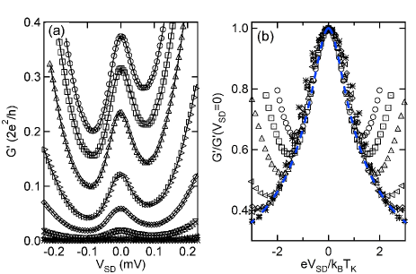
Observation of the signatures of the Kondo effect in magnetic field KlochanPRL11 indicates that the dot is small enough to see Kondo physics, and that we sit in a single Kondo valley where the dot occupancy is odd odd . The zero bias peak in Fig. 1(a) is superimposed on a rising background, which has been attributed to charge fluctuations in the mixed-valence regime in quantum dots GoldhaberPRL98 ; KretininPRB11 , or enhanced tunneling through a single barrier MartinMorenoJPCM92 . The conductance traces are asymmetric with respect to due to self-gating MartinMorenoJPCM92 , which we eliminate in our analysis by symmetrizing the experimental data with respect to V. We can estimate the Kondo temperature from the width of the zero bias peak. The theory PletyukhovPRL12 ; KretininPRB12 gives the full width at maximum as FW2/3M. As we go down from the top trace to the bottom in Fig. 1(a), the conductance drops by almost three orders of magnitude whereas the FW2/3M does not change significantly. Because depends exponentially on the coupling between the dot and the leads it should change drastically GoldhaberPRL98 . This implies that the dot is coupled asymmetrically to the leads with the more opaque barrier controlling the overall conductance while the more transparent barrier defines the Kondo temperature PustilnikJPC04 . When the conductance exceeds one of the barriers becomes completely transparent and we measure transport through a single barrier only, therefore to probe quantum dot physics we need to stay in the low conductance regime below . Thus the Kondo enhancement in these measurements cannot reach the unitary conductance limit .
We scale our data to numerically calculated in the limit of using as a single fitting parameter PletyukhovPRL12 , following a similar procedure to Ref. KretininPRB12 . To account for the asymmetric barriers we first normalize each ZBP trace by its zero bias value to obtain (even when the system is asymmetric this procedure is still valid as shown previously KretininPRB12 ; PletyukhovPRL12 , since the fit is primarily driven by the steepness of the conductance drop with applied source drain bias). Second, we plot both the experimental and the calculated as a function of scaled bias on a semi-log scale. Third, we shift each experimental trace along the -axis (adjust ) until it overlaps with the theoretical curve (because the ZBP is superimposed onto the rising background, the experimental data should always be above the calculations, particularly at large biases). The value of the shift required to make the experimental and calculated traces overlap then gives .
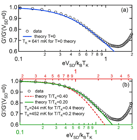
The results of scaling are presented in Fig. 1(b). Note that although the scaling is performed on a semi-log scale, the scaled data is shown on a linear scale to highlight the ZBP. At first sight the scaling of the experimental data (black symbols) to the calculated trace for (blue dashed line) looks very good, apart from the upturn due to the rising background in the experimental data at high bias (). However, closer inspection of Fig. 1(b) reveals that the experimental data are consistently above the calculations in the low bias window , where the agreement between theory and experiment should be best. An example of this is shown in Fig. 2(a), where a single experimental trace measured for V (the top trace in Fig. 1(a)) is fitted to the theory using as the only adjustable parameter. We can see that the experimental data lie above the theory for most of the low bias region. The fact that our data in Fig. 2(a) deviate from the calculated trace for suggests that the measurements are not in the low limit. Previous experiments KretininPRB11 which showed good agreement between the theory and experiment were performed in a system with . In contrast, we performed experiments on a system with smaller and higher measurement temperature so that we can reach higher .
The RTRG calculations of the differential conductance in Ref. PletyukhovPRL12 only consider the limiting cases where either the bias voltage or the temperature are zero. Very recently Reininghaus12 it has become possible to extend these calculations so that can be computed for all and . We have used 21 numerically calculated traces of in the range in steps of to find the best fit to each of our experimental traces. To demonstrate the improved agreement between the finite theory and the experimental data we show different calculated traces fitted to a single experimental trace in Fig. 2(b). We recall that the calculations for in Fig. 2(a) lie below the experimental data, because the ratio is too small to produce a good fit – on the semi-log axes of Fig 2(a) changing only shifts the experimental data sideways, without altering the slope of the curve. In Fig. 2(b) the same experimental data are plotted against both the top (red) the bottom (green) x-axis, along with the optimal theory calculations for (green solid line, bottom x-axis) and (red dashed line, top x-axis). Note that the experimental data in Fig. 2(b) can be read off either top or bottom axes, since is different for the experimental data when comparing with the two theoretical traces. For , we find very good agreement over the entire bias range, and extract mK. Increasing to 0.4 (red dashed line, top x-axis) fits the experiment well for but deviates significantly at higher biases, indicating that the ratio is too high. The error in is estimated by fitting the experimental trace to the two traces on each side of the optimal ratio and taking the average of the extracted .
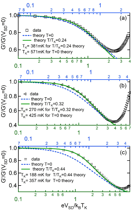
We perform the same fitting procedure for different side gate voltages, as shown in Fig. 3. We consistently get a better fit of experiment to theory when using calculations for (solid green lines, bottom x-axis), compared to (dashed blue lines, top x-axis). Using the values of and obtained from Figs. 2(b) and 3 we can estimate the hole temperature for each of the experimental traces. We obtain mK consistent with the temperature obtained by analysing Shubnikov de Haas oscillations from a GaAs two dimensional hole system performed in the same setup.
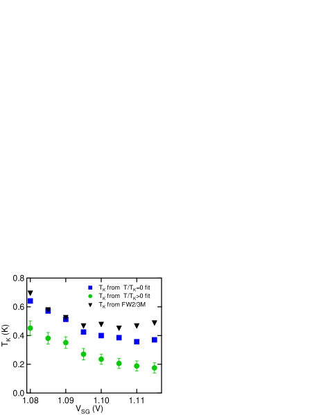
In Fig. 4 we compare the values of obtained from fitting to the and theory with those obtained from the peak width at maximum. From the shape of the universal conductance trace obtained from the theory (blue line in Fig. 1(b)), it can easily be seen that occurs at . Therefore the values of obtained from FW2/3M (black triangles) and the complete fit (blue squares) in Fig. 4 should coincide as long as is small. We can see in Fig. 4 that both traces follow the same trend, although the two traces separate from each other at larger , where is small. This is because the theory does not fit the experimental data well in this regime (see Fig. 3). Furthermore, both FW2/3M and the fit significantly overestimate the value of the real obtained from fitting to the finite theory (green circles). This shows that the zero bias peak width can not be used as an accurate estimate of the Kondo temperature at finite measurement temperatures.
To conclude, we have measured the zero bias peak in differential conductance in a hole quantum dot. We have scaled the experimental data and compared it to real time renormalization group calculations of differential conductance as a function of source-drain bias in the limit of zero temperature and at finite temperatures. Our experimental data show deviations from the calculations at low bias and are in very good agreement with the finite calculations. The Kondo temperature obtained from fitting the data to finite calculations is significantly lower than that extracted from the peak width at maximum and calculations.
This work was funded by the Australian Research Council through the DP, FT, APF and DORA schemes. Three co-authors (F.R, M.P., and H.S.) acknowledge the financial support from the DFG via the project FOR 723.
References
- (1) J. Kondo, Prog. Theor. Phys. 32, 37 (1964).
- (2) W. J. de Haas, J. de Boer and G. J. Van den Berg, Physica 1, 1115 (1933).
- (3) V. Madhavan, W. Chen, T. Jamneala, M. F. Crommie and N. S. Wingreen, Science 280, 567 (1998).
- (4) D. Goldhaber-Gordon, H. Shtrikman, D. Mahalu, D. Abusch-Magder, U. Meirav and M. A. Kastner, Nature 391, 156 (1998).
- (5) S. M. Cronenwett, T. H. Oosterkamp and L. P. Kouwenhoven, Science 281, 540 (1998).
- (6) L. P. Kouwenhoven and L. I. Glazman, Phys. World 14, 33 (2001).
- (7) D. Goldhaber-Gordon, J. Göres, M. A. Kastner, Hadas Shtrikman, D. Mahalu, and U. Meirav, Phys. Rev. Lett. 81, 5225 (1998).
- (8) M. Pletyukhov and H. Schoeller, Phys. Rev. Lett. 108, 260601 (2012).
- (9) A. V. Kretinin, H. Shtrikman, and D. Mahalu, Phys. Rev. B 85, 201301(R) (2012).
- (10) F. Reininghaus, M. Pletyukhov and H. Schoeller, in preparation (2013).
- (11) J. C. H. Chen, O. Klochan, A. P. Micolich, A. R. Hamilton, T. P. Martin, L. H. Ho, U. Zülicke, D. Reuter and A. D. Wieck, New J. Phys. 12, 033043 (2010).
- (12) O. Klochan, A. P. Micolich, A. R. Hamilton, K. Trunov, D. Reuter, and A. D. Wieck, Phys. Rev. Lett. 107, 076805 (2011).
- (13) K. Ensslin, Nat. Phys. 2, 587 (2006).
- (14) F. Sfigakis, C. J. B. Ford, M. Pepper, M. Kataoka, D. A. Ritchie, M. Y. Simmons, Phys. Rev. Lett. 100, 026807 (2008).
- (15) O. Klochan, W. R. Clarke, R. Danneau, A. P. Micolich, L. H. Ho, A. R. Hamilton, K. Muraki and Y. Hirayama, Appl. Phys. Lett. 89, 092105 (2006).
- (16) A series resistance of k due to ohmic contacts is used to calculate the voltage drop across the dot.
- (17) S. M. Cronenwett, H. J. Lynch, D. Goldhaber-Gordon, L. P. Kouwenhoven, C. M. Marcus, K. Hirose, N. S. Wingreen and V. Umansky, Phys. Rev. Lett. 88, 226805 (2002).
- (18) S. Sarkozy, F. Sfigakis, K. Das Gupta, I. Farrer, D. A. Ritchie, G. A. C. Jones and M. Pepper, Phys. Rev. B 79, 161307(R) (2009).
- (19) If the dot occupancy were even, the Kondo effect could also arise due to single-triplet degeneracy which can be tuned either by magnetic field SasakiNature00 or confinement potential KoganPRL03 . However, the even Kondo effect is characterized by nonmonotonic dependence of the ZBP in magnetic field and temperature GrangerPRB05 . We do not observe these signatures. Moreover in our device, the splitting of the ZBP in magnetic field is double the Zeeman energy, which is only expected for odd dot occupancy KlochanPRL11 .
- (20) S. Sasaki, S. De Franceschi, J. M. Elzerman, W. G. van der Wiel, M. Eto, S. Tarucha and L. P. Kouwenhoven, Nature 405, 764 (2000).
- (21) A. Kogan, S. Amasha, D. Goldhaber-Gordon, G. Granger, M. A. Kastner, and H. Shtrikman, Phys. Rev. Lett. 67, 113309 (2003).
- (22) G. Granger, M. A. Kastner, I. Radu, M. P. Hanson, and A. C. Gossard, Phys. Rev. B 72, 165309 (2005).
- (23) A. V. Kretinin, H. Shtrikman, D. Goldhaber-Gordon, M. Hanl, A. Weichselbaum, J. von Delft, T. Costi, and D. Mahalu, Phys. Rev. B 84, 245316 (2011).
- (24) L. Martin-Moreno, J. T. Nicholls, N. K. Patel and M. Pepper, J. Phys.: Condens. Matter 4, 1323 (1992).
- (25) M. Pustilnik and L. Glazman, J. Phys.: Condens. Matter 16, R513 (2004).