Unoccupied topological surface state in Bi2Te2Se
Abstract
Bias voltage dependent scattering of the topological surface state is studied by scanning tunneling microscopy/spectroscopy for a clean surface of the topological insulator Bi2Te2Se. A strong warping of constant energy contours in the unoccupied part of the spectrum is found to lead to a spin-selective scattering. The topological surface state persists to higher energies in the unoccupied range far beyond the Dirac point, where it coexists with the bulk conduction band. This finding sheds light on the spin and charge dynamics over the wide energy range and opens a way to designing opto-spintronic devices.
pacs:
73.20.-r, 72.10.Fk, 71.20.Nr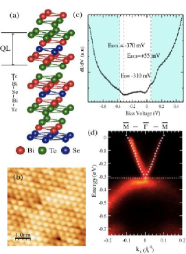
Three-dimensional topological insulators (3D TIs) represent a recently discovered state of matter, whose hallmark is the surface state in the absolute bulk energy gap, which has a spin non-degenerate Dirac-cone energy dispersion and helical spin texture Hasan10 ; Moore10 ; Fu07 ; Hasan11 ; Qi11 ; Okuda13 . The topological surface state (TSS) is protected by time-reversal symmetry and is robust against nonmagnetic perturbations.
Of all the 3D TIs, the most extensively studied is Bi2Se3 owing to its large energy gap and the single TSS Xia09 ; Kuroda10 . However, in spite of significant efforts to realize the surface isolated transport in Bi2Se3, the progress has been hampered by a too small surface contribution to the total conductance compared to the uncontrolled bulk contribution from the carrier doping due to the Se vacancies Butch10 ; Eto10 .
Here we focus on Bi2Te2Se, which has been theoretically predicted to be a 3D TI Lin-Lin Wang11 and confirmed by angle-resolved photoemission spectroscopy (ARPES) Arakane12 ; Neupane12 ; Niesner12 . A highly spin polarized TSS in Bi2Te2Se has been observed in recent spin-resolved ARPES (SARPES) measurements Miyamoto12 . Bi2Te2Se has an ordered tetradymite structure, derived from Bi2Te3 by replacing the central Te layer with a Se layer. Because here the Se atoms are confined in the central layer the formation of Se vacancies and the antisite defects between Bi and Te atoms is expected to be less probable Ren10 , which would suppress the bulk conductivity. Indeed, this compound has been found bulk insulating, and surface-derived quantum oscillations have been observed in a magnetotransport experiment Ren10 . This makes Bi2Te2Se very promising for spintronic applications.
Interband optical excitation of topological surface states by pulsed laser light is expected to generate longer-lived spin-polarized carriers at the surface Hosur11 ; Sobota12 . To understand the photoexcited spin and charge dynamics, knowledge of unoccupied topological surface state far above the Dirac point and the unoccupied bulk continuum is crucial. Note that photoelectron spectroscopy, with which most of the studies on topological insulators have been performed, cannot access unoccupied states or provide a direct information on the in-plane electron scattering. Thus, there has been a dearth of measurements on the unoccupied electronic states of 3D TIs, and the present study is motivated by the necessity of getting the information about the unoccupied spectrum.
Scanning tunneling microscopy (STM)/ spectroscopy (STS) has been widely used to study the surfaces of 3D TIs as the most surface sensitive technique providing direct information on the electronic structure of topological surface states and their scattering properties. One can unveil the spin structure of surface states through the presence or absence of standing waves both for occupied and unoccupied states. Fourier transformed images of the observed standing waves give bias-dependent scattering vectors in momentum space. For an isotropic TSS, the backscattering is strongly suppressed, while a spin-conserving scattering is allowed, and it has actually been observed in several topological insulators with warped constant energy contours (CECs) Fu09 ; Zhang09 ; Roushan09 ; Alpichshev10 ; Kim11 ; Beidenkopf11 ; Alpichshev12 ; Ye12 . A non-spin-conserving scattering can also occur if the time reversal symmetry is broken, i.e., in the presence of magnetic impurities Okada11 .
In this Letter, a quasiparticle interference pattern due to surface scattering is revealed on Bi2Te2Se with a low-temperature STM experiment over a wide sample bias energy range. A strong warping of CECs of the TSS explains the anisotropic spin-conserving scattering, which persists into the unoccupied state region, where the surface state coexists with bulk conduction band.
Our experiments were performed using an LT-STM (Omicron NanoTechnology GmbH) operated at 4.5 K in ultrahigh vacuum. Bi2Te2Se crystal was grown by modified vertical Bridgman method as described elsewhere Kokh05 . The STM images were obtained in a constant-current mode, and the differential conductance maps were measured simultaneously with recording the STM images using a standard lock-in technique. ARPES experiments were conducted using the synchrotron radiation at BL-7 equipped with a hemispherical photoelectron analyzer (VG-SCIENTA SES2002) of Hiroshima Synchrotron Radiation Center (HSRC). Samples were cleaved in ultra-high vacuum in situ at room temperature for the STM and at 10-20 K for ARPES measurement.
Similar to Bi2Se3 and Bi2Te3, Bi2Te2Se forms a rhombohedral crystal structure with the space group (, with the basis quintuple layer (QL) unit of Te-Bi-Se-Bi-Te, as depicted in Fig. 1(a). Inside the QL the bonds are predominantly ionic-covalent, and adjacent QLs are bound by van der Waals forces. Figure 1(b) is the atomic-resolution image ( mV, nA) of the Bi2Te2Se surface area of 5 nm nm. The scanning tunneling spectrum gives a measure of the local density of states near the Fermi energy as shown in Fig. 1(c). The resulting STS data were averaged over 10 spectra to improve statistics. The dashed lines show approximate energy locations of the top of the bulk valence band (BVB), Dirac point (DP) and the bottom of bulk conduction band (BCB) around the point. Figure 1(d) depicts the surface state energy dispersion of Bi2Te2Se measured by ARPES at the photon energy of eV [open circles indicate the band dispersion by our ab initio calculation (see Fig. 3) shifted downward by 0.24 eV to match the measured Dirac point position]. The DP energies from ARPES and STS spectra are equal Jia12 .
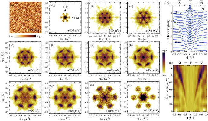
Figure 2(a) shows the differential conductance () map at a bias voltage of mV. It exhibits a standing wave spreading anisotropically around point defects. (All the spectroscopic maps at the bias voltages from to mV were obtained for the same surface without changing any other experimental parameters.) In order to get the momentum space information and obtain the scattering wave vectors, we have performed Fast Fourier Transformation (FFT) of the maps, see Figs. 2(b)–2(l). These scattering images provide information on bias-dependent quasiparticle interference. For bias voltages below mV the interference effect around the point defects is weak, and the FFT image shows a circular pattern with small vectors, which mainly come from the statistical noise. At mV, flower shaped patterns emerge [Fig. 2(b)] with six broad petals along . Note that the pattern becomes sharp and intensive at bias voltages between and mV. Starting with mV, with increasing the bias voltage the spots get gradually broader.
The evolution of the scattering vectors with is visualized by the FFT power profiles in Figs. 2(m) and 2(n). In Fig. 2(m), in the direction (rightwards) the scattering vectors become larger as increases, while there is practically no scattering along (leftwards). In Fig. 2(n) we show the ratio of the intensity profiles along and . The intensities ratio damps the background and makes the scattering more clear: we distinctly see the dispersion of with the bias voltage.
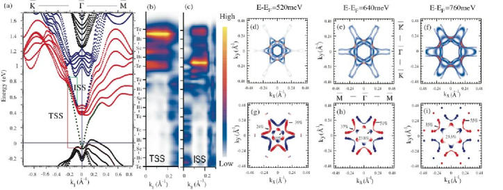
In order to elucidate the origin of scattering pattern and the effect of the helical spin texture of the TSS, we have performed a first-principles calculation of the electronic structure of a 7 formula units slab of Bi2Te2Se method . Figure 3(a) shows the band structure along (leftwards) and (rightwards). The magenta arrows show the energy and momentum ranges of the TSS, and the green arrows indicate the range of the inner surface state (ISS), which splits off from the top of the conduction band. Here, the DP is localized 0.065 eV below the calculated Fermi energy, i.e., the experimental energy scale is shifted by 0.24 eV relative to the theoretical scale. Figures 3(b) and 3(c) show the depth-momentum distribution (in the direction) of the charge density for the upper-cone TSS [Fig. 3(b)] and for the ISS [Fig. 3(c)]. The upper-cone surface state exists up to Å-1, and the ISS between 0.08 and 0.2 Å-1.
Figures 3(d)–3(f) show calculated momentum distributions of the spatially-resolved spectral density at three constant energies . The function is defined as a sum over all (discrete) states with energy and Bloch vector weighted with the probability of finding the electron in this state in the surface region: . (For the sake of presentation, the function is replaced by a Gaussian of 0.05 eV full width at half maximum.) The integral over the surface region comprises two outermost atomic layers and vacuum.
The angular distribution of the spin polarization perpendicular to the surface for the two surface states, TSS and ISS, is shown in Figs. 3(g)–3(i). Here the net spin density is integrated over a half of the slab, and the net spin is normalized to the electron charge in the integration region.
The TSS is somewhat stronger localized than the ISS [cf. Figs. 3(b) and 3(c)], and it exhibits a higher out-of-plane spin polarization. It is most interesting that the magnitude of the out-of-plane spin polarization of the TSS may be as large as 55%.
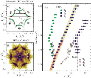
The bias-dependent quasiparticle scattering is characterized by scattering vectors that connect the vectors of the initial and final scattering states at the CEC. Figure 4(a) shows schematic CECs of the TSS. Three characteristic scattering vectors denoted as , , and explain the features in Fig. 4(b). The most intense croissant-shaped features can only be explained by and , which connect two flat segments of the contour as shown in Fig. 4(a). Other scattering features along the direction characterized by and , can also be explained as due to the warping of TSS. The scattering originating from ISS can be excluded because its CEC has no parallel fragments to cause a large joint density of states, and its convex shape does not lead to the croissant-shaped structures.
To clarify the relation between experimental and theoretical results, the intensity maxima of the FFT power profiles in the direction in Fig. 2(m) are compared with the values extracted from the slab calculation, see Fig. 4(c). By shifting the calculated points upward by 0.1 eV we were able to reproduce all the experimentally observed scattering features. (A discrepancy of the same order between the two photon photoemission measurements of the unoccupied Dirac cone and calculations was reported in Ref. [12].)
The presence of the FFT features in the direction and their absence in the direction tells us that the scattering is strongly spin selective. This scattering scenario holds for the whole energy interval from to mV above the Fermi energy, and no significant surface to bulk scattering is observed, in contrast to Bi2Se3, for which a bulk-related scattering has been reported Kim11 . This indicates that a coupling of the TSS with the bulk continuum states is negligible even in the unoccupied region, which energetically overlaps with the bulk conduction band.
In conclusion, our scanning tunneling microscopy/spectroscopy experiment and the first-principles calculation of Bi2Te2Se reveal a scattering pattern that originates from the strongly warped constant energy contours of the topological surface state with substantial out-of-plane spin polarization. The topological surface state is thus found to survive up to energies far above the Dirac point. This finding provides a deeper understanding of optically excited spin and charge dynamics at the surface of topological insulators.
STM and ARPES measurements were performed with the approval of the Proposal Assessing Committee of HSRC (Proposal No.11-B-40, No.10-A-32). This work was financially supported by KAKENHI (Grant No. 20340092, 23340105), Grant-in-Aid for Scientific Research (B) of JSPS and by RFBR, research project No. 13-02-92105 a. The authors acknowledge partial support from the Spanish Ministerio de Ciencia e Innovación (Grant No. FIS2010-19609-C02-02).
References
- (1) M.Z. Hasan and C.L. Kane, Rev. Mod. Phys. 82, 3045 (2010).
- (2) J.E. Moore, Nature 464, 194 (2010).
- (3) L. Fu, C.L. Kane, and E.J. Mele, Phys. Rev. Lett. 98, 106803 (2007).
- (4) X.L. Qi and S.C. Zhang, Rev. Mod. Phys. 83, 1057 (2011).
- (5) M.Z. Hasan and J.E. Moore, Ann. Review. Condensed Matter Physics.2, 55-78 (2011).
- (6) T. Okuda and A. Kimura, J. Phys. Soc. Jpn 82, 021002 (2013).
- (7) Y. Xia, D. Qian, D. Hsieh, L. Wray, A. Pal, H. Lin, A. Bansil, D. Grauer, Y. S. Hor, R. J. Cava, and M. Z. Hasan, Nature Phys. 5, 398 (2009).
- (8) K. Kuroda, M. Arita, K. Miyamoto, M. Ye, J. Jiang, A. Kimura, E.E. Krasovskii, E.V. Chulkov, H. Iwasawa, T. Okuda, K. Shimada, Y. Ueda, H. Namatame, and M. Taniguchi, Phys. Rev Lett 105, 076802 (2010).
- (9) N. P. Butch, K. Kirshenbaum, P. Syers, A. B. Sushkov, G. S. Jenkins, H. D. Drew, and J. Paglione, Phys. Rev. B 81, 241301(R) (2010).
- (10) K. Eto, Z. Ren, A. A. Taskin, K. Segawa, and Y. Ando, Phys. Rev. B 81, 195309 (2010).
- (11) L.L. Wang, and D.D. Johnson, Phys. Rev. B 83, 241309(R) (2011)).
- (12) T. Arakane, T. Sato, S. Souma, K. Kosaka, K. Nakayama, M. Komatsu, T. Takahashi, Z. Ren, K. Segawa, and Y. Ando, Nature Comms. 3, 636 (2012).
- (13) M. Neupane, S.-Y. Xu, L. A. Wray, A. Petersen, R. Shankar, N. Alidoust, C. Liu, A. Fedorov, H. Ji, J.M. Allred, Y.S. Hor, T.R. Chang, H.T. Jeng, H. Lin, A. Bansil, R.J. Cava, and M.Z. Hasan, Phys. Rev. B 85, 235406 (2012).
- (14) D. Niesner, Th. Fauster, S.V. Eremeev, T.V. Menshchikova, Yu.M. Koroteev, A.P. Protogenov, E.V. Chulkov, O.E. Tereshchenko, K.A. Kokh, O. Alekperov, A. Nadjafov, and N. Mamedov, Phys. Rev. B. 86, 205403 (2012).
- (15) K. Miyamoto, A. Kimura, T. Okuda, H. Miyahara, K. Kuroda, H. Namatame, M. Taniguchi, S.V. Eremeev, T.V. Menshchikova, E.V. Chulkov, K.A. Kokh, and O.E. Tereshchenko, Phys. Rev. Lett. 109, 166802 (2012).
- (16) Z. Ren, A.A. Taskin, S. Sasaki, K. Segawa, and Y. Ando, Phys. Rev. B. 82, 241306(R) (2010).
- (17) P. Hosur, Phys. Rev. B 83, 035309 (2011)
- (18) J.A. Sobota, S. Yang, J.G. Analytis, Y.L. Chen, I.R. Fisher, P.S. Kirchmann, and Z.X. Shen, Phys. Rev. Lett. 108, 117403 (2012)
- (19) T. Zhang, P. Cheng, X. Chen, J.F. Jia, X.C. Ma, K. He, L.L. Wang, H.J. Zhang, X. Dai, Z. Fang, X.C. Xie, and Q.K. Xue, Phys. Rev. Lett. 103, 266803 (2009).
- (20) L. Fu, Phys. Rev. Lett. 103, 266801 (2009).
- (21) P. Roushan, J. Seo, C.V. Parker, Y.S. Hor, D. Hsieh, D. Qian, A. Richardella, M.Z. Hasan, R.J. Cava and A. Yazdani, Nature 460, 1106 (2009).
- (22) Z. Alpichshev, J.G. Analytis, J.H. Chu, I.R. Fisher, Y.L. Chen, Z.X. Shen, A. Fang, and A. Kapitulnik, Phys. Rev. Lett. 104, 016401 (2010).
- (23) S. Kim, M. Ye, K. Kuroda, Y. Yamada, E.E. Krasovskii, E.V. Chulkov, K. Miyamoto, M. Nakatake, T. Okuda, Y. Ueda, K. Shimada, H. Namatame, M. Taniguchi, and A. Kimura, Phys. Rev. Lett. 107, 056803 (2011).
- (24) H. Beidenkopf, P. Roushan, J. Seo, L. Gorman, I. Drozdov, Y.S. Hor, R.J. Cava and A. Yazdani, Nature 7, 939-943 (2011).
- (25) Z. Alpichshev, R.R. Biswas, A.V. Balatsky, J.G. Analytis, J.H. Chu, I.R. Fisher, and A. Kapitulnik, Phys. Rev. Lett. 108, 206402 (2012).
- (26) M. Ye, S.V. Eremeev, K. Kuroda, E.E. Krasovskii, E.V. Chulkov, Y. Takeda, Y. Saitoh, K. Okamoto, S.Y. Zhu, K. Miyamoto, M. Arita, M. Nakatake, T. Okuda, Y. Ueda, K. Shimada, H. Namatame, M. Taniguchi, and A. Kimura, Phys. Rev. B, 85, 205317 (2012).
- (27) Y. Okada, C. Dhital, W.W. Zhou, E.D. Huemiller, H. Lin, S. Basak, A. Bansil, Y.B. Huang, H. Ding, Z. Wang, S.D. Wilson, and V. Madhavan, Phys. Rev. Lett. 106, 206805 (2011).
- (28) K.A. Kokh, B.G. Nenashev, A.E. Kokh, and G.Y. Shvedenkov, J. Crystal Growth 275, e2129 (2005).
- (29) S. Jia, H. Beidenkopf, I. Drozdov, M.K. Fuccillo, J. Seo,J. Xiong, N.P. Ong, A. Yazdani, and R.J. Cava Phys. Rev. B. 86, 165119 (2012).
- (30) Self-consistent calculation within the local density approximation were performed with the full-potential augmented plane wave method described in E.E. Krasovskii, F. Starrost, and W. Schattke, Phys. Rev. B 59, 10504 (1999).