Bimodal substrate biasing to control -Al2O3 deposition during reactive magnetron sputtering
Abstract
Al2O3 thin films have been deposited at substrate temperatures between 500∘C to 600∘C by reactive magnetron sputtering using an additional arbitrary substrate bias to tailor the energy distribution of the incident ions. The films were characterized by X-ray diffraction (XRD) and Fourier transform infrared spectroscopy (FTIR). The film structure being amorphous, nanocrystalline, or crystalline was correlated with characteristic ion energy distributions. The evolving crystalline structure is connected with different levels of displacements per atom (dpa) in the growing film as being derived from TRIM simulations. The boundary between the formation of crystalline films and amorphous or nanocrystalline films was at 0.9 dpa for a substrate temperature of 500∘C. This threshold shifts to 0.6 dpa for films grown at 550∘C.
I Introduction
Reactive magnetron sputtering (RMS) is a prominent technique to deposit many thin film materials as for examples oxides and nitrides using metal targets and the addition of oxygen and/or nitrogen as a reactive component to the argon plasma gas Koski et al. (1999); Clarke (1994); Wallin et al. (2008); Zywitzki et al. (1996). The film stoichiometry and its structure can be adjusted by controlling the ion-to-neutral ratio in the film forming growth flux and the energy of the incident ions given by the ion energy distribution function (IED). Incident ions may enhance the adatom mobility and promote thereby crystallinity and/or a certain crystalline orientation Wallin et al. (2008); Rosén et al. (2005a, b). This is often quantified by the energy per deposited atom . This energy depends on the ion energy and on the ion-to-neutral ratio / in the growth flux with = /. Here, is the flux of incident ions and the total flux of incorporated atoms in the film.
Under variation of the average parameter and the ion to neutral ratio , it was shown by Adibe et al. Adibi et al. (1993) and Petrov et al. Petrov et al. (1993) that the average energy per incorporated atom is no universal parameter for the formation of titanium nitride (Ti0.5Al0.5N). However, in addition to Musil et al. Musil et al. (1990), the average energy per incorporated atom is suggested to define the formation of crystallinity by several authors Poulek et al. (1989, 1991); Grigorov et al. (1991).
Recently, we devised an experiment to very accurately control the growth flux and the energy distribution of the incident ions Prenzel et al. (2013a) by keeping the average energy per deposited atom , the average energy of the incident ions , the total ion flux and the ion-to-neutral ratio constant, but changing only the ion energy distribution (IED), for details see Prenzel et al. (2013a).
We applied this concept to RMS of Al2O3 films as a prominent material with applications ranging from microelectronics, wear resistant coatings to catalytic surfaces Zywitzki et al. (1996). The most common phases of Al2O3 are the - and -phase. -Al2O3 with its hexagonal closed package (hcp) Gautier et al. (1994) structure is often used as hard coating on machining tools.
In 2005 Rosen et al. have reviewed phase formation data reported for vapor phase deposited alumina Rosén et al. (2005b) and summarize that the majority of authors observe that the crystalline growth temperature appears to be reduced as the mobility of surface species through energetic ion bombardment is increased. In 2010 Jiang et al. report an alpha alumina formation temperature of 560∘C by utilizing large ion fluxes during PACVD Jiang et al. (2010) as discharge power densities of 19 Wcm-2 resulted in an increase in the energy and the flux of the bombarding species towards the growing film, as well as in a more efficient precursor dissociation Jiang et al. (2010). In the same year, Sarakinos et al. reported an alpha alumina formation temperature of 720∘C by cathodic arc deposition Sarakinos et al. (2010) for substrate bias potentials between -40 V and -200 V. Based on ab initio molecular dynamics calculations Music et al. (2011) subplantation of the impinging Al is identified to cause significantly larger irradiation damage and hence larger mobility in the gamma alumina as compared to alpha alumina. Consequently, the enhanced mobility results in the growth of the alpha phases at the expense of the gamma phase.
From the above discussion it can be learned that in addition to the well-established mechanism of ion bombardment mediated surface diffusion the previously overlooked subplantation mechanism Sarakinos et al. (2010); Music et al. (2011) was suggested to be relevant for the formation of crystalline alumina thin films.
Previously Prenzel et al. (2013a), we monitored the transition from X-ray amorphous to -alumina to assess the influence of the ion energy distribution on thin film growth, indicating that typically one displacement per incorporated atom (dpa) is necessary for that transition to occur. In this paper, we expand the data set and measured a comprehensive set of XRD and FTIR data to also identify nanocrystalline samples, which appear as being crystalline in the FTIR measurement although they are still X-ray amorphous. Based on this large data set, the hypothesis of characteristic dpa levels to allow for a certain structural transitions in the films can be more thoroughly tested. Formation of amorphous films, of nanocrystalline films or of X-ray -crystalline Al2O3 films was observed by FTIR and XRD. It has to be emphasized that our parameter interval is restricted to only the variation of the ion energy distribution function of the incoming ions and the substrate temperature. Therefore, it is possible to isolate the effect of the transfer of kinetic energy on the film growth.
II Experimental methods
II.1 Film deposition
Thin aluminum oxide films were deposited using a dual frequency magnetron sputter experiment employing 13.56 MHz and 71 MHz for plasma generation, as described in detail in Prenzel et al. (2013a). The discharge was operated at 0.1 Pa at a constant argon flow rate of 9 sccm. The base pressure in the deposition chamber was 210-5 Pa. Based on Rosén et al. (2006); Prenzel et al. (2013a) this is expected to lead to H incorporation of 2at.%. The incorporated H atoms from water in the residual gas Schneider et al. (1999) is small enough that the effect of incorporated water in the films can be neglected. A feedback loop regulated the oxygen flow into the chamber to avoid target poisoning by monitoring a constant intensity of the Al I emission line at 396.2 nm using a narrow band pass filter and a photomultiplier. The adjusted oxygen partial pressure in the deposition chamber was determined as 8.610-3 Pa in average. Thereby, stoichiometric Al2O3 coatings were prepared as being verified by ex-situ X-ray Photoelectron Spectroscopy (XPS).
The distance between target and the p-doped Si(100) substrate was 50 mm. The substrate temperature during the deposition process was regulated to 500 ∘C, 550 ∘C and 600 ∘C, respectively. The substrate temperature was directly measured by analyzing the temperature dependent refraction index of silicon at 632.8 nm by ellipsometry Kroesen et al. (1991). This is non intrusive and measures directly the surface temperature. Any thermocouple at the substrate holder my read a different temperature due to improper thermal contacts. Pyrometry remain ambiguous because the emissivity of the coated silicon wafer is not well defined and silicon becomes transparent in the infrared wavelength range at high temperatures.
II.2 Substrate biasing and ion energy distribution
The substrate electrode was intentionally biased to tailor the ion energy distribution function (IEDF) of the incident ions. Rectangular waveforms were generated by a waveform generator and amplified using a broadband amplifier. A coupling capacitor was used to connect the biasing signal to the substrate electrode.
The kinetic energy of the impinging ions is controlled as follows: a rectangular biasing signal can be divided into an on-time () and an off-time (). The frequency of the pulsing is given as . In our experiments, the on-time was fixed to a value of 500 ns and a change in frequency of the applied biasing signal was realized by changing the off-time only. Thereby, the fluence () of energetic ions during growth remains identical in all experiments. The maximum ion energy , in case of collisionless sheaths, corresponds to the voltage drop between the biasing signal and the plasma potential. Consequently, was used as parameter to uniquely characterize the ion bombardment during film growth.
A typical bias signal for a frequency =1.01 MHz and a maximum voltage of is shown in Figure 1 (a) as being measured at the substrate electrode by an oscilloscope. The signal is not perfectly rectangular due to the low pass filtering effect of the coupling capacitor. The resulting IEDF was simulated from the voltage signal at the electrode by a sheath model, as described by Shihab et al. Shihab et al. (2012). The resulting IEDF is shown in Figure 1 (b) as ion flux per ion energy interval versus ion energy.
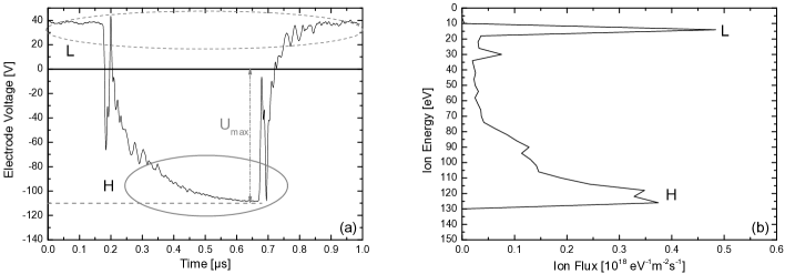
Two prominent peaks (regions H and L in Figure 1) in the IEDF can be identified. The maximum ion energy within the IEDF in Figure 1 (b) corresponds to the maximum bias voltage applied to the substrate electrode (region H). During this time period, ions are accelerated by the voltage drop between plasma potential (18 V) and maximum bias voltage to the substrate electrode (). This results in a maximum ion energy of . In addition, a low energetic peak (region L) originates from ions accelerated during the off-time with an ion energy corresponding to the voltage drop between plasma potential and floating potential.
Frequencies between 0.80 MHz and 1.60 MHz were applied to regulate the ratio between the ion flux at high vs. low ion energies. The ion energy of the high energetic peak within the IEDF was adjusted to a desired ion energy by a defined tailoring of the maximum bias voltage . Therefore, any ratio between the two peaks within the IEDF and any position of the high energetic peak can be reached by tailoring frequency and maximum bias voltage .
The energy impact during film growth is usually defined by the mean energy per incorporated atom depending on the maximum ion energy of the ions , the total growth flux , the ion flux and the duty cycle according to:
| (1) |
The growth flux is defined by the incorporated flux of aluminum and oxygen atoms during Al2O3 film formation. This is deduced from the total film thickness, as measured ex situ by a profilometer, divided by the overall deposition time. The growth rate expressed in nm s-1 is converted into the growth flux in cm-2s-1 using the density of the film and the average mass of Al2O3 via . A residual thickness inhomogeneity of 4% is observed which converts into an error of the growth flux of 5%.
Because XRD analysis of our films exhibits good crystalline quality of -alumina (see below), the film density value from literature of =3.66 gcm-3 as being reported by Levin et al. Levin and Brandon (1998) seems to have reasonable good agreement with our films and is taken for the further discussion.
Finally, the ion flux to the substrate surface is required when determining the mean ion energy per incorporated atom . The ion flux was measured using a retarding field analyzer within a previous work Prenzel et al. (2013b). It was determined as =13.5 m-2s-1.
II.3 Thin film analysis
Phase formation was studied by XRD with a Bruker D8 General Area Diffraction System (GADDS) on the deposited Al2O3 thin films. The incident angle of the beam was 15∘ and the analyzed 2 angle range was 20∘ to 75∘. The applied voltage and current settings were 40 kV and 40 mA, respectively. Three different peaks which can be associated to the phase of Al2O3 are identified in the diffraction patterns of our samples. The (311) direction can be found within the XRD pattern at an angle of 37.30∘. Moreover, peaks at 45.86∘ and 67.03∘ are identified as (400) and (440) orientations, respectively. Peak positions agree with the JCDPS file number 10-0425 for -Al2O3 at 45.9∘ and 67.0∘.
Further analysis of the Al2O3 samples was realized by ex situ FTIR transmission measurements using a Bruker IFS 66/S spectrometer. A polarizer was placed in front of the sample, so that only s polarized light reached the sample. The angle of incidence normal to the surface was 60∘. Measurements were performed in the wavenumber range between 400 cm-1 and 6,000 cm-1. Background spectra of non-coated silicon wafers were used.
Brüesch et al. Bruesch et al. (1984) investigated FTIR spectra of amorphous and -aluminum oxide. The evolution of a sharp peak (or dip within transmission spectra) at 950 cm-1 is characteristic for -Al2O3. Further broad oscillations at lower wavenumbers being characterized by Chu et al. Chu et al. (1988) at 357 cm-1, 536 cm-1 and 744 cm-1 were identified.
XRD and FTIR assess the crystallinity of the samples on distinct length scales: (i) in XRD, the coherent scattering of the incident X-radiation from a crystal leads to pronounced peaks in the XRD diffractogram. In case of nanocrystalline samples, significant line broadening occurs which complicates the evaluation of X-ray profiles. As a consequence, the distinction between crystalline and amorphous samples depends on the employed diagnostic method and nanocrystalline samples may not be detected by XRD. (ii) in FTIR, the signal originates from the absorption of single Al-O bonds at a frequency depending on the configuration of the next neighbors. If nanocrystallites are formed, characteristic LO or TO phonon peaks may appear in the infrared spectrum, whereas the coherent overlap of the scattered light in XRD by crystalline region and amorphous sites may still show X-ray amorphous diffraction patterns.

Based on the different measurement principles of XRD and FTIR, the transition from amorphous, nanocrystalline, to crystalline samples can be assessed, as illustrated in Figure 2 for films deposited at different deposition conditions, as described below: (i) Figure 2 show the spectra for amorphous films, since no distinct peaks in the XRD diffractogram (a) and no sharp absorption for TO phonon at approximately 950 cm-1 is found (b) ; (ii) Figure 2 shows an XRD diffractogram (c) for a nanocrystalline film, which appears XRD-amorphous. Infrared absorption at a wavenumber of 950 cm-1 reflects the formation of nanocrystallites, which is shown in Figure 2 (d); (iii) Figure 2 shows an XRD diffractogram (e) for a crystalline film with sharp peaks in the XRD diffractogram at position characteristic to -alumina. In addition to the XRD signature, pronounced absorptions for TO phonon become also visible in the IR spectrum (f).
It is important to note that the identification of the nanocrystalline phase from a comparison of the XRD and FTIR data remains ambiguous for very few cases, because the sharpness of the TO-phonon peak in FTIR is not as distinct as the analysis of the diffraction peaks in the XRD diffractogram. Those samples are marked in the presented data sets.
III Results and Discussion
A large set of 73 samples was prepared in the substrate temperature range between 500 ∘ and 600 ∘C at a pressure of 0.1 Pa. The IEDF was tailored using frequencies in the range between 0.80 MHz and 1.60 MHz for the pulsed bias and maximum bias voltages between -25 V to -280 V. The range of operating parameters and the resulting average energies are listed in Table 1. The samples were analyzed ex situ by XRD and FTIR with respect to their structure. The deposition is characterized by the maximum ion energy and the average energy per incorporated atom . Figure 4 shows the results for the amorphous samples (open triangle), the nanocrystalline samples (half filled squares), and the crystalline samples (solid squares) for three different substrate temperatures of 500 ∘C (Figure 4a), of 550 ∘C (Figure 4b), and of 600 ∘C (Figure 4c). The dashed areas in Figure 4 indicate deposition parameters, which are not reasonable, because the average energy cannot be larger than the maximum energy .
Finally, the correlation of the deposition parameters with the structure of the deposited films may be affected by nucleation phenomena.
| Deposition/ | Adjusted values |
|---|---|
| Biasing parameter | |
| Temperature T | 500 ∘C, 550 ∘C, 600 ∘C |
| Biasing frequency f | 0.80 MHz, 1.01 MHz, |
| 1.20 MHz, 1.40 MHz, | |
| 1.60 MHz | |
| Mean energy per incor- | 10 eV…30 eV…60 eV |
| porated atom | |
| Maximum Biasing | -25 V…-280 V |
| voltage | |
| Maximum ion | 7 eV…262 eV |
| energy |
The data in Figure 4 indicate that crystalline films are usually obtained if the average energy and the maximum energy are above a certain threshold. This becomes more critical at lower substrate temperatures, where also amorphous films are observed at low and . The films at intermediate values for and show nanocrystalline behavior. At a temperature of 600 ∘C, aluminum oxide is deposited in the phase even for very low ion bombardment and only very few samples remain amorphous.
This rough analysis already illustrates that an increasing energy input during film growth induces a transition of the film structure from an amorphous to a nanocrystalline and finally to a crystalline structure. This is in agreement with the current general understanding of energetic film deposition.
The ion-induced formation of a nanometer size crystal or the phase could be induced by displacement events within a collision cascade. These displacements generate mobility and may turn enable the the formation of a crystalline structure. This very general picture can be tested with our data by comparing the samples, as plotted in Figure 4, with TRIM simulations Möller and Eckstein (1984) to calculate the displacements per incorporated atoms in the growing films.
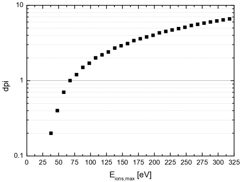
TRIM simulations were performed for argon ions, which initiate a collision cascade in an stoichiometric Al2O3 film. Surface binding energies for Al atoms and O were assumed as 3.36 eV and 2.00 eV, respectively. A density of 3.66 g cm-3 was assumed Levin and Brandon (1998) and mono energetic argon ions with energies between 28 eV and 308 eV. This corresponds to maximum voltages at the substrate electrode of -10 V to -300 V, respectively. The displacement per ion (dpi) for the different ion energies was calculated and plotted versus ion energy in Figure 3. No distinction between displacing aluminum or oxygen is made. A threshold energy of 32 eV for aluminum oxide is necessary to induce a displacement event within the Al2O3 film. Ion bombardment by a rectangular bias signal establishes two distinct peaks with different ion energies impinging onto the substrate surface. Ions with low energies with 18 eV are below the threshold to initiate a displacement within the aluminum oxide film. Only ions with ion energies above the critical value of 32 eV have enough energy to initiate a displacement within the film. The low energetic ions are accelerated within the off period of the bias signal, whereas high energetic ions are produced during the on-time of the signal. Therefore, only ions from the high energetic peak within the IEDF account to the dpi within the Al2O3 films.
The displacements per ion (dpi) are converted into displacements per atom (dpa) during film growth by multiplying it with the ratio between energetic ion fluence per puls and the growth fluence :
| (2) |
Equation 1 can be combined with eq. 2 yielding a dependence of the dpa level on the control parameters and :
| (3) |
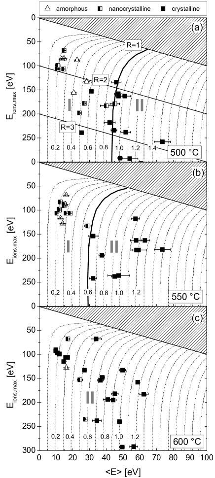
The resulting dpa levels are then plotted as contour lines in Figure 4, separating the samples into two regions (indicated as I and II in Figure 4) for different substrate temperatures:
-
•
Deposition at 500∘C: in region I (dpa 0.9), most films are amorphous or nanocrystalline, while in region II (dpa 0.9) all films are crystalline. The threshold may also be aligned to a certain mean energy per deposited atom , which might be detected at 43 eV.
The observation of different dpa threshold values being necessary for a structural transformation from amorphous to nanocrystalline or from nanocrystalline to amorphous, respectively, is consistent with the current understanding of energetic film formation: a certain energy input is required to allow for the formation of a specific phase of the material.
The separation of the samples into different regions depending on the dpa level is similar to a criterion solely based on the average energy per deposited atoms for ion energies above 150 eV. This is illustrated by the contour lines being almost parallel to the y-axis due to the linear relationship between dpi and ion energy at high energies (see Figure 3).
The separation of the samples into different regions may be regarded in more detail. Petrov et al. Adibi et al. (1993) made an observation indicating that besides an average energy, the absolute energy has to be at least high enough for the incident ion to penetrate into the material and to displace atoms. This criterion, however, is already the basis of the dpa contour plots. In our case, we still see structural changes although the dpa level remains the same if we follow individual contour lines at the border between the regions. The only remaining difference for those samples is the fact that the dissipated energy is distributed among several species for 200 eV, but dissipated only by a few atoms for 150 eV. The number of atoms that dissipate the ion energies are given by the flux ratios, which are additionally plotted in Figure 4 (a).
-
•
Deposition at 550∘C: in region I (dpa 0.6) most films are amorphous or nanocrystalline, while above a dpa value of 0.6 all films become crystalline. One can clearly see that the boundaries between amorphous or nanocrystalline films to crystalline films shifts to lower dpa levels. This is consistent with the current understanding of film formation that less ion-induced mobility is required at higher substrate temperatures.
-
•
Deposition at 600∘C: all films become crystalline, irrespective of the dpa level. Apparently, the substrate temperature is high enough so that even very small dpa levels are already sufficient to induce the formation of crystalline films. A clear transition between region II and I cannot be identified anymore in our data set.
A close inspection of Figure 4 shows that very few samples are not located consistently in the respective region - crystalline films in region I instead of II, or amorphous/ nanocrystalline films in region II instead of I. This deviation may be induced by two effects, the variation in the nucleation process or the variation in the grain size distribution:
-
(a)
In nucleation a delicate competition between amorphous and crystalline phases can occur, where small deviations in the initial condition such as substrate morphology, contamination etc. may lead to growth of completely different film structures.
-
(b)
The distinction between crystalline and amorphous films by XRD depends very sensitive on the grain size distribution. For small grains or low grain size density, a crystalline phase might easily be undetected by XRD. However, it should be emphasized that the vast majority of samples can consistently be located in region I and II, respectively.
The mapping of the film structure on the parameters of the energy input during film growth expressed in and and its comparison to the dpa levels that are induced during film growth shows good agreement. One may extrapolate this scaling to Al2O3 deposition in general, to predict the film structure in the plasma based on the operating parameters of the system. The description of the IEDF with a maximum ion energy is only reasonable for rectangular bias. The underlying important quantity however is the dpa level in the film, which can be uniquely calculated using TRIM calculations for any ion energy distribution function. The extrapolation of the proposed scaling approach for other bias waveforms is currently under way.
IV Conclusion
Al2O3 thin films have been deposited at substrate temperatures between 500∘C and 600∘C by reactive magnetron sputtering using an additional arbitrary substrate bias to tailor the energy distribution of the incident ions. The formation of crystalline films as opposed to amorphous or nanocrystalline films depends on a critical threshold of 0.9 displacement per incorporated atom at 500∘C substrate temperature. This threshold shifts to 0.6 dpa with increasing substrate temperature to 550∘C. One can conclude that for fixed neutral to ion fluxes to the film surface, the dpa value is a predictor for the formation of crystalline Al2O3 films. The driving mechanism of the formation of crystalline structures is the enhanced mobility of surface atoms due to Ar ion bombardment. As the dpa value increases, the formation temperature of crystalline Al2O3 thin films is decreased.
V Acknowledgment
The authors would like to thank Norbert Grabkowski for his technical support within the experimental setup.
This project is supported by DFG (German Research Foundation) within the framework of the Special Research Field SFB-TR 87 and the Research Department ‘Plasmas with Complex Interactions’ at Ruhr-Universit t Bochum.
Finally, the authors like to thank M. Shihab and R.P. Brinkmann for their support in modeling the ion energy distribution functions for a given bias signal at the electrodes.
References
- Koski et al. (1999) K. Koski, J. Hölsä, and P. Juliet, Thin Solid Films 339, 240 (1999), ISSN 00406090, URL http://linkinghub.elsevier.com/retrieve/pii/S0040609098012322.
- Clarke (1994) P. J. Clarke, Journal of Vacuum Science & Technology A: Vacuum, Surfaces, and Films 12, 594 (1994), ISSN 07342101, URL http://link.aip.org/link/?JVA/12/594/1&Agg=doi.
- Wallin et al. (2008) E. Wallin, T. I. Selinder, M. Elfwing, and U. Helmersson, EPL (Europhysics Letters) 82, 36002 (2008), ISSN 0295-5075, URL http://stacks.iop.org/0295-5075/82/i=3/a=36002?key=crossref.fada472bbee68e1835daeba98887bc9a.
- Zywitzki et al. (1996) O. Zywitzki, G. Hoetzsch, F. Fietzke, and K. Goedicke, Surface and Coatings Technology 82, 169 (1996), ISSN 02578972, URL http://linkinghub.elsevier.com/retrieve/pii/0257897295002707.
- Rosén et al. (2005a) J. Rosén, J. M. Schneider, and K. Larsson, Solid State Communications 135, 90 (2005a), ISSN 00381098, URL http://linkinghub.elsevier.com/retrieve/pii/S0038109805003078.
- Rosén et al. (2005b) J. Rosén, S. Mráz, U. Kreissig, D. Music, and J. M. Schneider, Plasma Chemistry and Plasma Processing 25, 303 (2005b), ISSN 0272-4324, URL http://www.springerlink.com/index/10.1007/s11090-004-3130-y.
- Adibi et al. (1993) F. Adibi, I. Petrov, J. E. Greene, L. Hultman, and J.-E. Sundgren, Journal of Applied Physics 73, 8580 (1993), ISSN 00218979, URL http://jap.aip.org/resource/1/japiau/v73/i12/p8580_s1http://link.aip.org/link/JAPIAU/v73/i12/p8580/s1&Agg=doi.
- Petrov et al. (1993) I. Petrov, F. Adibi, J. E. Greene, L. Hultman, and J.-E. Sundgren, Applied Physics Letters 63, 36 (1993), ISSN 00036951, URL http://apl.aip.org/resource/1/applab/v63/i1/p36_s1http://link.aip.org/link/APPLAB/v63/i1/p36/s1&Agg=doi.
- Musil et al. (1990) J. Musil, S. Kadlec, V. Valvoda, R. Kužel, and R. Černý, Surface and Coatings Technology 43-44, 259 (1990), ISSN 02578972, URL http://linkinghub.elsevier.com/retrieve/pii/025789729090079R.
- Poulek et al. (1989) V. Poulek, J. Musil, R. Černý, and R. Kuzel, Thin Solid Films 170, L55 (1989), ISSN 00406090, URL http://linkinghub.elsevier.com/retrieve/pii/0040609089907384.
- Poulek et al. (1991) V. Poulek, J. Musil, V. Valvoda, and R. Kuzel, Thin Solid Films 196, 265 (1991), ISSN 00406090, URL http://linkinghub.elsevier.com/retrieve/pii/004060909190370D.
- Grigorov et al. (1991) G. Grigorov, I. Martev, M. Stoyanova, J.-L. Vignes, and J.-P. Langeron, Thin Solid Films 198, 169 (1991), ISSN 00406090, URL http://linkinghub.elsevier.com/retrieve/pii/004060909190335U.
- Prenzel et al. (2013a) M. Prenzel, A. Kortmann, A. von Keudell, F. Nahif, J. M. Schneider, M. Shihab, and R. P. Brinkmann, Journal of Physics D: Applied Physics 46, 084004 (2013a), ISSN 0022-3727, URL http://stacks.iop.org/0022-3727/46/i=8/a=084004?key=crossref.3977466fb5377ee9197df775317007f8.
- Gautier et al. (1994) M. Gautier, G. Fenaud, L. Pham Van, B. Villette, M. Pollak, N. Thromat, F. Jollet, and J.-p. Duraud, Journal of the American Ceramic Society 77, 323 (1994), ISSN 0002-7820, URL http://doi.wiley.com/10.1111/j.1151-2916.1994.tb06999.x.
- Jiang et al. (2010) K. Jiang, K. Sarakinos, S. Konstantinidis, and J. M. Schneider, Journal of Physics D: Applied Physics 43, 325202 (2010), ISSN 0022-3727.
- Sarakinos et al. (2010) K. Sarakinos, D. Music, F. Nahif, K. Jiang, a. Braun, C. Zilkens, and J. M. Schneider, physica status solidi (RRL) - Rapid Research Letters 4, 154 (2010), ISSN 18626254, URL http://doi.wiley.com/10.1002/pssr.201004133.
- Music et al. (2011) D. Music, F. Nahif, K. Sarakinos, N. Friederichsen, and J. M. Schneider, Applied Physics Letters 98, 111908 (2011), ISSN 00036951, URL http://link.aip.org/link/APPLAB/v98/i11/p111908/s1&Agg=doi.
- Rosén et al. (2006) J. Rosén, E. Widenkvist, K. Larsson, U. Kreissig, S. Mráz, C. Martinez, D. Music, and J. M. Schneider, Applied Physics Letters 88, 191905 (2006), ISSN 00036951, URL http://link.aip.org/link/APPLAB/v88/i19/p191905/s1&Agg=doi.
- Schneider et al. (1999) J. M. Schneider, B. Hjörvarsson, X. Wang, and L. Hultman, Applied Physics Letters 75, 3476 (1999), ISSN 00036951, URL http://link.aip.org/link/APPLAB/v75/i22/p3476/s1&Agg=doi.
- Kroesen et al. (1991) G. M. W. Kroesen, G. S. Oehrlein, and T. D. Bestwick, Journal of Applied Physics 69, 3390 (1991), ISSN 00218979, URL http://link.aip.org/link/JAPIAU/v69/i5/p3390/s1&Agg=doi.
- Shihab et al. (2012) M. Shihab, D. Ziegler, and R. P. Brinkmann, Journal of Physics D: Applied Physics 45, 185202 (2012), ISSN 0022-3727, URL http://stacks.iop.org/0022-3727/45/i=18/a=185202?key=crossref.32271c08a9a890ec429db0cee1751d5b.
- Levin and Brandon (1998) I. Levin and D. Brandon, Journal of the American Ceramic Society 81, 1995 (1998), ISSN 00027820, URL http://dx.doi.org/10.1111/j.1151-2916.1998.tb02581.xhttp://doi.wiley.com/10.1111/j.1151-2916.1998.tb02581.x.
- Prenzel et al. (2013b) M. Prenzel, A. Kortmann, A. von Keudell, F. Nahif, J. M. Schneider, M. Shihab, and R. P. Brinkmann, Journal of Physics D: Applied Physics 46, 084004 (2013b), ISSN 0022-3727, URL http://stacks.iop.org/0022-3727/46/i=8/a=084004?key=crossref.3977466fb5377ee9197df775317007f8.
- Bruesch et al. (1984) P. Bruesch, R. Koetz, H. Neff, and L. Pietronero, Physical Review B 29, 4691 (1984).
- Chu et al. (1988) Y. T. Chu, J. B. Bates, C. W. White, and G. C. Farlow, Journal of Applied Physics 64, 3727 (1988), ISSN 00218979, URL http://jap.aip.org/resource/1/japiau/v64/i7/p3727_s1http://link.aip.org/link/JAPIAU/v64/i7/p3727/s1&Agg=doi.
- Möller and Eckstein (1984) W. Möller and W. Eckstein, Nuclear Instruments and Methods in Physics Research Section B: Beam Interactions with Materials and Atoms 2, 814 (1984), ISSN 0168583X, URL http://linkinghub.elsevier.com/retrieve/pii/0168583X84903215.