Role of MgO barriers for spin and charge transport in Co/MgO/graphene non-local spin-valve devices
Abstract
We investigate spin and charge transport in both single and bilayer graphene non-local spin-valve devices. An inverse dependence of the spin lifetime on the carrier mobility is observed in devices with large contact resistance area products (). Furthermore, we observe an increase of with increasing values demonstrating that spin transport is limited by spin dephasing underneath the electrodes. In charge transport, we measure a second contact-induced Dirac peak at negative gate voltages in devices with larger values demonstrating different transport properties in contact covered and bare graphene parts. We argue that the existence of the second Dirac peak complicates the analysis of the carrier mobilities and the spin scattering mechanisms.
Graphene has drawn strong attention because of measured spin diffusion length of some m at room temperature. While most spin transport devices only exhibit spin lifetimes up to several hundred picoseconds at room temperature Tombros et al. (2007); Dlubak et al. (2012); Han and Kawakami (2011); Han et al. (2012); Guimaraes et al. (2012); Swartz et al. (2013); Birkner et al. (2013); Jo et al. (2011); Neumann et al. (2013) there are only few reports with spin lifetimes above one nanosecond.Wojtaszek et al. (2013); Maassen et al. (2012a); Yang et al. (2011) Nevertheless, all experimental values of the spin lifetimes are some orders of magnitude shorter than theoretically predicted Huertas-Hernando et al. (2009); Ertler et al. (2009) indicating that in present devices spin transport is limited by extrinsic sources of spin scattering. These include spin-orbit coupling by adatoms, edge effects and ripples. Wojtaszek et al. (2013); Huertas-Hernando et al. (2009); Swartz et al. (2013); Pi et al. (2010); Castro Neto and Guinea (2009); Zhang and Wu (2012); Avsar et al. (2011) Additionally, spin scattering may result from the underlying substrate or the spin injection and detection contacts. Ertler et al. (2009); Han et al. (2010); Maassen et al. (2012b) The importance of the latter might be indicated by recent electron spin resonance (ESR) experiments on graphene nanoribbons and small flakes that were only weakly coupled to the substrate and had no electrodes. Rao et al. (2012); Augustyniak-Jablokow et al. (2013) Interestingly, the measured spin lifetimes of localized spin states are at least while the estimated spin lifetimes of conduction electrons are , which is larger than any reported values from electrical Hanle spin precession measurements.
In this Rapid Communication, we investigate the influence of MgO barriers on spin and charge transport properties by fabricating both single layer (SLG) and bilayer graphene (BLG) non-local spin-valve devices with variable contact resistance area products of the MgO/Co electrodes. We explore the relationship between spin lifetime and charge carrier mobility in SLG and find a similar dependence as seen in previous spin transport studies on exfoliated bilayer graphene (BLG) devices. Yang et al. (2011) This dependence is only seen in samples with . In fact, we observe that devices with long additionally exhibit a second Dirac peak in charge transport, which stems from the electrodes. This contact-induced Dirac peak overlaps with the Dirac peak of the bare graphene which complicates the analysis of the carrier mobility and thus complicates a clear assignment of the dominant spin scattering mechanism in graphene. For devices with low we find an overall strong decrease of showing that transparent contacts yield additional spin dephasing in graphene underneath the contacts.
We have fabricated exfoliated SLG and BLG devices on ()/ wafers. The number of graphene layers is determined by optical contrast measurement which is calibrated by Raman spectroscopy. After e-beam lithography we use molecular beam epitaxy to first grow an MgO spin injection/detection barrier with varying thicknesses from up to followed by thick ferromagnetic Co contacts. The rather thick barrier is necessary due to the fact that MgO on graphene growths in the Volmer-Weber mode (island formation) if no wetting layer is used. Wang et al. (2008) We have evidence that even devices with large contacts that show non-linear differential I-V-curves still exhibit pinholes in the barrier. 111Paper in preparation. Thus the exact current distribution through the contact areas is unknown, which complicates the assignment of the correct values.Nagashio et al. (2010) For the sake of simplicity, we assume a homogeneous current distribution for our analysis.
All transport measurements are performed under vacuum condition at room temperature (RT) using standard lock-in techniques. 222See Supplemental Material for a more detailed description of device fabrication, measurement methods and supporting measurements. The highly doped -wafer is used as a backgate which allows changing the charge carrier density in the graphene sheet according to the established capacitor model Novoselov et al. (2004) with , being the applied gate voltage and being the gate voltage position of the maximum resistivity at the charge neutrality point, also called Dirac point. By a linear fit of the conductance , we extract the charge carrier mobility at an electron density of . Hanle spin precession measurements are performed in standard non-local 4-terminal geometry and are fitted by a simplified analytical solution Fabian et al. (2007); Johnson and Silsbee (1988) of the steady-state Bloch-Torrey equation: 22footnotemark: 2
| (1) |
where is the net spin vector, the Larmor frequency, the spin diffusion constant and the transverse spin lifetime. Recent experiments indicate that the effective g-factor in graphene-based spin transport devices may differ from the free electron value at low temperatures after a hydrogen treatment. McCreary et al. (2012) As ESR measurements for untreated graphene show even for low temperatures Rao et al. (2012); Augustyniak-Jablokow et al. (2013) and we also restrict ourselves to RT, we assume for all devices in this study.
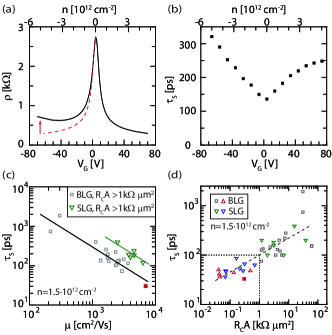
In Figs. 1(a)-(c) we show typical transport data for a SLG device with .22footnotemark: 2 We first note that there is a strong electron-hole asymmetry in charge transport (Fig. 1(a)) as seen by the increase of the graphene resistivity for hole doping towards large negative values. Its origin will be discussed further below. Spin lifetimes are extracted from Hanle curves,Yang et al. (2011) which have been measured in perpendicular magnetic fields. The gate voltage dependent times in Fig. 1(b) show a minimum at the Dirac point and increase with both electron and hole doping. This general trend is observed for most large devices.
We next evaluate the dependence of on the electron mobility at for all SLG devices in Fig. 1(c) (green triangles) on a log-log scale. For easier comparison we include results on BLG (gray squares in Fig. 1(c)), which some of us had previously measured. Yang et al. (2011) The most striking observation is that like in BLG depends inversely on in our SLG devices. This relationship was previously attributed to the dominance of D’yakonov-Perel’ (DP) like spin dephasing in graphene.
Remarkably, SLG devices exhibit longer spin lifetimes than BLG devices of equal mobility. The vertical offset between SLG and BLG in Fig. 1(c) can be analyzed within the DP spin dephasing mechanism. For this we replace the momentum scattering time in the DP formula with the Boltzmann expression of the mobility and take the logarithm: Fabian et al. (2007)
| (2) |
where e is the elementary charge, the effective Larmor frequency which is dependent on the spin-orbit coupling and is the effective mass. With this expression it is obvious that the vertical offset in Fig. 1(c) can either result from a smaller effective mass or a smaller overall spin-orbit coupling strength in the SLG devices. We note that SLG is expected to exhibit massless Dirac fermions near the Dirac point only in simple tight-binding approximations. It has been shown that even the small intrinsic spin-orbit coupling in SLG gives rise to a small effective mass of the charge carriers,Gmitra et al. (2009); Konschuh et al. (2010) which supports our simple approach in Eq. 2. Even stronger effects are expected from extrinsic sources such as contacts, adatoms, and the underlying substrate. Zhang and Wu (2012); Castro Neto and Guinea (2009); Ertler et al. (2009) As all experimental values of are well below theoretical predictions, we expect that spin relaxation and dephasing is governed by extrinsic sources in present devices. Because of the dominant extrinsic contribution to the spin-orbit coupling slight changes in the fabrication steps between the BLG and SLG devices (in our case another batch of wafer, another resist for lithography) might be the reason for the observed offset in the lifetime. These changes in sample fabrication may also explain the overall larger carrier mobilities in the new series of SLG devices seen in 1(c) (no device under ).
In the following, we will focus on the influence of on . Several groups have suggested to use high resistive tunneling contacts to avoid the backflow of charge carrier spins into the ferromagnetic electrodes which otherwise yields a reduction of the spin lifetime.Popinciuc et al. (2009); Han et al. (2010); Dlubak et al. (2012); Maassen et al. (2012b) As mentioned above, all of our SLG devices exhibit large values. Revisiting our previous BLG measurements also reveals values above for almost all BLG data points in Fig. 1(c) (gray squares). Only the BLG device with the highest mobility (red, filled square in Fig. 1(c)) has low contacts with a flat differential d/d-curve. 22footnotemark: 2
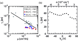
At first sight this red data point seems to follow the DP like trend of the large BLG devices. To explore this in further detail we fabricated additional SLG and BLG samples with a thinner MgO barrier but otherwise same fabrication procedure. All of those show (Fig. 1(d) blue and red data points). As seen in Fig. 2(a), they exhibit strongly reduced values which vary between 30 and (upward pointing triangles for BLG and downward pointing ones for SLG) and lie well below all large devices with no significant difference between SLG and BLG devices. Furthermore, the data do not follow the 1/ dependence. It is therefore obvious that devices with exhibit short spin lifetimes in which the above dependence of the large devices is hidden by an additional spin dephasing channel which most likely results from the contacts.
The strong influence of low contacts on the spin transport can also be seen by the charge density dependence of (Fig. 2(b)), which is similar for all low devices. In contrast to all large devices at room temperature (see Fig. 1(b)), does not increase away from the Dirac point, but it rather decreases and may increase again at larger carrier densities. Although we presently do not understand this qualitative change in the density dependence, we note that such a decrease of has previously also been observed in BLG devices with large contacts at low temperatures. Yang et al. (2011)
While we have seen that devices with low and large values show a distinctly different mobility dependence of the spin lifetime (Fig. 1(c) and 2(a)), we now discuss the dependence of on which is shown in Fig. 1(d) for all devices with measured values. We note that even within a single device the respective values for different contacts may vary significantly. The plotted values in Fig. 1(d) are thus mean values of the respective injector and detector contacts of each device. Remarkably, we observe a significant increase of with for all devices suggesting that the contacts are even the bottleneck for the large devices. However, these devices also showed the pronounced inverse dependence of on (see Fig. 1(c)). It is therefore interesting to study if the influence of the contacts also becomes evident in charge transport.
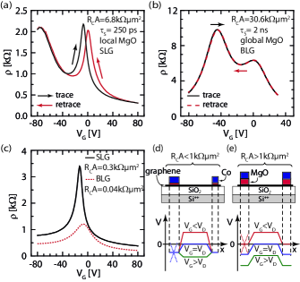
In Figs. 3(a) to (c), we summarize the gate voltage dependent graphene resistivity for both large and low SLG and BLG devices. While we only observe one Dirac peak around zero gate voltage in all low devices (see Fig. 3(c)), we typically observe a second Dirac peak at larger negative gate voltages for SLG and BLG devices with large (Figs. 3(a) and (b)). Such a second Dirac peak has already been observed in spin-valve devices by another group.Vera-Marun et al. (2012) The resistivity ratio of both Dirac peaks varies significantly from device to device. Not all large devices show the maximum of the second Dirac peak for (cp. to Fig. 1(a)). But the general trend is that the separation between both Dirac peaks gets smaller for devices with larger . Consistent with the additional scaling between and , the smallest peak separation has been observed in the device with the longest of (Fig. 3(b)).
The left Dirac peak most likely results from the magnetic electrodes while the right Dirac peak is due to charge transport through the graphene sheet between the electrodes. This notion is supported by hysteresis measurements when comparing different devices with local and global MgO barriers. In the former case MgO is only deposited underneath the ferromagnetic electrodes (see Fig. 3(a) for corresponding SLG device) while in the latter case MgO completely covers the graphene flake (see Fig. 3(b)). A hysteresis is only observed for the right Dirac peak in the device with local MgO barriers (Fig. 3(a)). It can originate from a thin water film on top of the graphene flake. Wang et al. (2010) Although we measure under vacuum condition, such a hysteresis is initially always observed before the water will eventually evaporate after a few hours. However, no hysteresis for the left Dirac peak at negative gate voltages is observed. If this peak results from the contact area, this is also expected as water cannot cover the graphene underneath the contact area. Consistent with this assignment, we do not observe any hysteresis for global MgO devices (see Fig. 3(b)).
We next link the appearance of the second Dirac peak to the measured spin lifetime and the contact characteristics. It is well known that the contact material has a great influence on the transport properties in graphene. Scanning photocurrent microscopy experiments, for example, directly probe contact-induced doping and show Fermi level pinning from metallic electrodes. Mueller et al. (2009) A gate voltage dependent doping profile of the electrostatic potential for devices with low ohmic contacts is depicted in Fig. 3(d). Here equals to the position of the Fermi level in the graphene band structure. Although this profile can successfully explain an electron-hole-asymmetry in the resistivity,Nouchi and Tanigaki (2010) which we also observe in our low devices, it cannot explain the second Dirac peak as the carrier density underneath the electrodes is not affected by the gate voltage.
As noted above, there is an island growth of our MgO barriers. In particular for thin barriers this favors the formation of conducting Co pinholes with presumably direct contact of the Co to the graphene layer. As shown by recent angle-resolved photoemission spectroscopy the Dirac cone of graphene is strongly shifted into the valence band for Co/graphene interfaces and its band hybridizes with 3d bands of Co near the Fermi level.Varykhalov and Rader (2009); Varykhalov et al. (2012) This hybridization is consistent with the Fermi level pinning in our low devices. It furthermore might account for the reduced spin lifetimes in Fig. 2(a) (red and blue data points) as the injected spins might be scattered by the 3d states in the graphene layer.
For large devices with thicker MgO oxide barriers the formation of pinholes is suppressed. Accordingly the 3d-hybridization of Co with graphene states gets diminished which can yield longer spin lifetimes. Furthermore, we expect a gradual depinning of the Fermi level. Together with the weaker Co induced n-doping with increasing oxide thicknessGiovannetti et al. (2008); Bokdam et al. (2013) this also explains the appearance of the second Dirac peak. This situation is illustrated in Fig. 3(e) where the backgate voltage now also tunes the carrier density underneath the contacts. We note that the transition between pinning and depinning should in principal be continuous with increasing . In other words, the appearance of the second Dirac peak does not necessarily imply a complete depinning. Considering the spatially inhomogeneous barrier thickness due to the Volmer-Weber island growth and remaining pinholes even for large devices all current devices might not be in the regime of complete depinning. The rough Co/MgO interface may also result in inhomogeneous local magnetic fields which can be an additional source of spin dephasing.Dash et al. (2011) Finally, we do not observe a systematic dependence of the amplitude of the spin signal on the values 22footnotemark: 2, which excludes a backflow of spins into the ferromagnetic electrode as a possible explanation of the observed dependence on .Popinciuc et al. (2009); Han et al. (2010); Maassen et al. (2012b)
Next we address the calculation of for devices with a second Dirac peak. In Figs. 1(d) and 2(a) we determined and from the right Dirac peak which we attribute to the bare graphene part. This might be a good approach for devices with only one Dirac peak (Fig. 3(c)) or for devices where the left Dirac peak is strongly separated in gate voltage as in Fig. 1(a). In particular for devices with long , however, the two Dirac peaks are not well separated but strongly overlap as seen in Figs. 3(a) and 3(b) for large SLG and BLG devices, respectively. This overlapping has significant influence on the slope of the right Dirac peak at (). The smaller the separation between both Dirac peaks becomes the smaller the respective slope and carrier mobility will be. We note that this results in an underestimation of the mobility of the bare graphene part. It is important to emphasize that the contact-induced left Dirac peak might thus partially be responsible for the decrease in observed carrier mobility for devices with longer spin lifetimes.
There are more elaborated models to determine carrier mobilities including contact-induced pinning and depinning of the Fermi level and the respective potential profiles of the graphene along the device. Thiele et al. (2010); Jimenez (2011); Nouchi and Tanigaki (2011); Li et al. (2011); Vera-Marun et al. (2012) However, there are too many unknown quantities which currently hinder to extract reliable values for the respective carrier mobilities in the different graphene parts from a single gate dependent resistivity measurement.22footnotemark: 2 Without further measurements of the potential profile we thus cannot give a more precise evaluation of the influence of the contact induced Dirac peak on the carrier mobility. This, on the other hand, would be important for identifying intrinsic spin dephasing mechanisms in graphene. Our findings show that the understanding of spin transport in graphene based non-local spin-valve devices requires independent understanding of both spin and charge transport properties which may significantly differ in graphene underneath the spin injection and detection electrodes and graphene between the electrodes. Guimaraes et al. (2012)
In summary, we have studied spin and charge transport in graphene-based non-local spin-valves by tuning the values of MgO injection/detection barriers. For low contacts, there is a significant spin dephasing in graphene underneath the contacts, while SLG and BLG devices with large values show long spin lifetimes at RT. The latter devices exhibit a second Dirac peak at negative gate voltages. As the peak separation is smallest for devices with the longest spin lifetimes, it might partially account for the observed dependence of .
This work was supported by DFG through FOR 912.
References
- Tombros et al. (2007) N. Tombros, C. Jozsa, M. Popinciuc, H. T. Jonkman, and B. J. van Wees, Nature 448, 571 (2007).
- Dlubak et al. (2012) B. Dlubak, M.-B. Martin, C. Deranlot, B. Servet, S. Xavier, R. Mattana, M. Sprinkle, C. Berger, W. A. De Heer, F. Petroff, A. Anane, P. Seneor, and A. Fert, Nat Phys 8, 557 (2012).
- Han and Kawakami (2011) W. Han and R. K. Kawakami, Phys. Rev. Lett. 107, 047207 (2011).
- Han et al. (2012) W. Han, J.-R. Chen, D. Wang, K. M. McCreary, H. Wen, A. G. Swartz, J. Shi, and R. K. Kawakami, Nano Letters 12, 3443 (2012).
- Guimaraes et al. (2012) M. H. D. Guimaraes, A. Veligura, P. J. Zomer, T. Maassen, I. J. Vera-Marun, N. Tombros, and B. J. van Wees, Nano Letters 12, 3512 (2012).
- Swartz et al. (2013) A. G. Swartz, J.-R. Chen, K. M. McCreary, P. M. Odenthal, W. Han, and R. K. Kawakami, Phys. Rev. B 87, 075455 (2013).
- Birkner et al. (2013) B. Birkner, D. Pachniowski, A. Sandner, M. Ostler, T. Seyller, J. Fabian, M. Ciorga, D. Weiss, and J. Eroms, Phys. Rev. B 87, 081405 (2013).
- Jo et al. (2011) S. Jo, D.-K. Ki, D. Jeong, H.-J. Lee, and S. Kettemann, Phys. Rev. B 84, 075453 (2011).
- Neumann et al. (2013) I. Neumann, J. Van de Vondel, G. Bridoux, M. V. Costache, F. Alzina, C. M. S. Torres, and S. O. Valenzuela, Small 9, 156 (2013).
- Wojtaszek et al. (2013) M. Wojtaszek, I. J. Vera-Marun, T. Maassen, and B. J. van Wees, Phys. Rev. B 87, 081402 (2013).
- Maassen et al. (2012a) T. Maassen, J. J. van den Berg, N. IJbema, F. Fromm, T. Seyller, R. Yakimova, and B. J. van Wees, Nano Letters 12, 1498 (2012a).
- Yang et al. (2011) T.-Y. Yang, J. Balakrishnan, F. Volmer, A. Avsar, M. Jaiswal, J. Samm, S. R. Ali, A. Pachoud, M. Zeng, M. Popinciuc, G. Güntherodt, B. Beschoten, and B. Özyilmaz, Phys. Rev. Lett. 107, 047206 (2011).
- Huertas-Hernando et al. (2009) D. Huertas-Hernando, F. Guinea, and A. Brataas, Phys. Rev. Lett. 103, 146801 (2009).
- Ertler et al. (2009) C. Ertler, S. Konschuh, M. Gmitra, and J. Fabian, Phys. Rev. B 80, 041405 (2009).
- Pi et al. (2010) K. Pi, W. Han, K. M. McCreary, A. G. Swartz, Y. Li, and R. K. Kawakami, Phys. Rev. Lett. 104, 187201 (2010).
- Castro Neto and Guinea (2009) A. H. Castro Neto and F. Guinea, Phys. Rev. Lett. 103, 026804 (2009).
- Zhang and Wu (2012) P. Zhang and M. W. Wu, New Journal of Physics 14, 033015 (2012).
- Avsar et al. (2011) A. Avsar, T.-Y. Yang, S. Bae, J. Balakrishnan, F. Volmer, M. Jaiswal, Z. Yi, S. R. Ali, G. Güntherodt, B. H. Hong, B. Beschoten, and B. Özyilmaz, Nano Letters 11, 2363 (2011).
- Han et al. (2010) W. Han, K. Pi, K. M. McCreary, Y. Li, J. J. I. Wong, A. G. Swartz, and R. K. Kawakami, Phys. Rev. Lett. 105, 167202 (2010).
- Maassen et al. (2012b) T. Maassen, I. J. Vera-Marun, M. H. D. Guimarães, and B. J. van Wees, Phys. Rev. B 86, 235408 (2012b).
- Rao et al. (2012) S. S. Rao, A. Stesmans, J. van Tol, D. V. Kosynkin, A. Higginbotham-Duque, W. Lu, A. Sinitskii, and J. M. Tour, ACS Nano 6, 7615 (2012).
- Augustyniak-Jablokow et al. (2013) M. A. Augustyniak-Jablokow, K. Tadyszak, M. Mackowiak, and S. Lijewski, Chemical Physics Letters 557, 118 (2013).
- Wang et al. (2008) W. H. Wang, W. Han, K. Pi, K. M. McCreary, F. Miao, W. Bao, C. N. Lau, and R. K. Kawakami, Applied Physics Letters 93, 183107 (2008).
- Note (1) Paper in preparation.
- Nagashio et al. (2010) K. Nagashio, T. Nishimura, K. Kita, and A. Toriumi, Appl. Phys. Lett. 97, 143514 (2010).
- Note (2) See Supplemental Material for a more detailed description of device fabrication, measurement methods and supporting measurements.
- Novoselov et al. (2004) K. S. Novoselov, A. K. Geim, S. V. Morozov, D. Jiang, Y. Zhang, S. V. Dubonos, I. V. Grigorieva, and A. A. Firsov, Science 306, 666 (2004).
- Fabian et al. (2007) J. Fabian, A. Matos-Abiague, C. Ertler, P. Stano, and I. Zutic, ACTA PHYSICA SLOVACA 57, 565 (2007).
- Johnson and Silsbee (1988) M. Johnson and R. H. Silsbee, Phys. Rev. B 37, 5312 (1988).
- McCreary et al. (2012) K. M. McCreary, A. G. Swartz, W. Han, J. Fabian, and R. K. Kawakami, Phys. Rev. Lett. 109, 186604 (2012).
- Gmitra et al. (2009) M. Gmitra, S. Konschuh, C. Ertler, C. Ambrosch-Draxl, and J. Fabian, Phys. Rev. B 80, 235431 (2009).
- Konschuh et al. (2010) S. Konschuh, M. Gmitra, and J. Fabian, Phys. Rev. B 82, 245412 (2010).
- Popinciuc et al. (2009) M. Popinciuc, C. Józsa, P. J. Zomer, N. Tombros, A. Veligura, H. T. Jonkman, and B. J. van Wees, Phys. Rev. B 80, 214427 (2009).
- Vera-Marun et al. (2012) I. J. Vera-Marun, V. Ranjan, and B. J. van Wees, Nat Phys 8, 313 (2012).
- Wang et al. (2010) H. Wang, Y. Wu, C. Cong, J. Shang, and T. Yu, ACS Nano 4, 7221 (2010).
- Mueller et al. (2009) T. Mueller, F. Xia, M. Freitag, J. Tsang, and P. Avouris, Phys. Rev. B 79, 245430 (2009).
- Nouchi and Tanigaki (2010) R. Nouchi and K. Tanigaki, Applied Physics Letters 96, 253503 (2010).
- Varykhalov and Rader (2009) A. Varykhalov and O. Rader, Phys. Rev. B 80, 035437 (2009).
- Varykhalov et al. (2012) A. Varykhalov, D. Marchenko, J. Sanchez-Barriga, M. R. Scholz, B. Verberck, B. Trauzettel, T. O. Wehling, C. Carbone, and O. Rader, Phys. Rev. X 2, 041017 (2012).
- Giovannetti et al. (2008) G. Giovannetti, P. A. Khomyakov, G. Brocks, V. M. Karpan, J. van den Brink, and P. J. Kelly, Phys. Rev. Lett. 101, 026803 (2008).
- Bokdam et al. (2013) M. Bokdam, P. A. Khomyakov, G. Brocks, and P. J. Kelly, Phys. Rev. B 87, 075414 (2013).
- Dash et al. (2011) S. P. Dash, S. Sharma, J. C. Le Breton, J. Peiro, H. Jaffrès, J.-M. George, A. Lemaître, and R. Jansen, Phys. Rev. B 84, 054410 (2011).
- Thiele et al. (2010) S. A. Thiele, J. A. Schaefer, and F. Schwierz, Journal of Applied Physics 107, 094505 (2010).
- Jimenez (2011) D. Jimenez, Electron Devices, IEEE Transactions on 58, 4377 (2011).
- Nouchi and Tanigaki (2011) R. Nouchi and K. Tanigaki, Japanese Journal of Applied Physics 50, 070109 (2011).
- Li et al. (2011) Q. Li, E. H. Hwang, E. Rossi, and S. Das Sarma, Phys. Rev. Lett. 107, 156601 (2011).