Coherent Flux Tunneling Through NbN Nanowires
Abstract
We demonstrate evidence of coherent magnetic flux tunneling through superconducting nanowires patterned in a thin highly disordered NbN film. The phenomenon is revealed as a superposition of flux states in a fully metallic superconducting loop with the nanowire acting as an effective tunnel barrier for the magnetic flux, and reproducibly observed in different wires. The flux superposition achieved in the fully metallic NbN rings proves the universality of the phenomenon previously reported for . We perform microwave spectroscopy and study the tunneling amplitude as a function of the wire width, compare the experimental results with theories, and estimate the parameters for existing theoretical models.
pacs:
74.78.Na, 42.50.PqIntroduction. Superconducting electrical circuits containing Josephson tunnel junctions have provided an ideal testing ground for investigating the quantum mechanics of macroscopic variables, starting with the observation of quantum coherence of the superconducting phase difference across a Josephson junction martinis87 and leading to the development of superconducting qubits clarke08 . Recently, it was realized that due to the fundamental charge–phase duality exhibited by Josephson devices, exactly dual physics can be observed in circuits containing narrow nanowires of highly disordered superconductors in which coherent quantum phase slips (CQPS) can have a significant probability amplitude mooij06 . Thermally activated phase slips (PS) of the order parameter, corresponding to passage of a quantum of magnetic flux over the energy barrier represented by the wire, are a well-known origin of resistance below the critical temperature in superconducting wires little67 ; tinkhambook ; arutyunov08 . At the lowest temperatures, transport measurements indicate a transition to PS by incoherent quantum tunneling giordano88 ; bezryadin00 ; altomare06 ; zgirski08 . Very recently CQPS was observed directly for the first time in strongly disordered nanowires embedded into superconducting loops astafiev12 , demonstrating the concept of a PS flux qubit mooij05 , dual to the single Cooper pair box nakamura99 . However, several basic questions remain open, e.g., universality and reproducibility in different materials. Moreover, strongly disordered superconductors such as exhibit a number of properties different from conventional superconductors, in particular the role of dissipation driessen12 , which make the study of QPS an interesting problem in itself.
In this Letter, we report the observation of coherent flux superpositions in fully metallic NbN loops, each containing a nanowire section as the tunnel barrier for magnetic flux (cf. Fig. 1). We observe the behavior in several loops on the same chip, characterize the dependence of the flux tunneling on the wire width, and compare the measurement results with the expected exponential dependence on the barrier width. Each of the two main findings of this work, (i) demonstration of coherent flux tunneling in a material different from and (ii) its wire-width dependence are of significant importance. They are crucial for developing more involved CQPS devices hriscu11 ; kerman12 ; hongisto12 ; lehtinen12 , utilizing physics dual to conventional Josephson ones. Reproducing the flux superposition in the fully metallic superconducting rings shows that CQPS is a generic property of strongly disordered superconductors with large gap. Furthermore our results show an exponential dependence on the wire width that further proves the tunneling nature of the phase slip process which can be visualized as a virtual vortex crossing the wire. It is remarkable that such process that involves the rearrangement of many electrons remain nevertheless coherent.
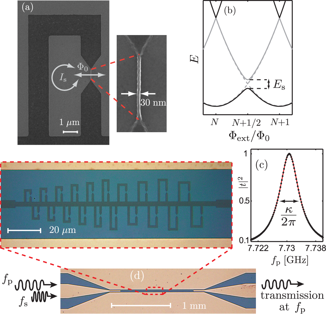
The device. The scanning electron micrograph of a typical loop in Fig. 1 illustrates the working principle of a PS flux qubit mooij05 ; mooij06 ; matveev02 ; arutyunov12 . A loop of NbN with nominal area and high kinetic inductance is placed in a perpendicular magnetic field . Due to flux quantization in superconducting loops tinkhambook , the total flux through the loop is an integer () multiple of the magnetic flux quantum , and the energy of the loop is , expressed in terms of the external flux with and the inductive energy lgnote . The CQPS process in the nanowire, described by the amplitude , lifts the degeneracy of the fluxoid states and at . The resulting energy band diagram is shown in Fig. 1 , characterized by an avoided crossing of magnitude mooij05 .
At the ground and first excited states correspond to symmetric and antisymmetric superpositions of and , respectively. The energy splitting of this effective two level system is . Here, , with the persistent current and , gives the difference away from the degeneracy. To probe and hence , we couple the loop to a coplanar NbN resonator via a section of shared kinetic inductance [bottom loop edge in Fig. 1], enabling readout of multiple qubits located close to each other on a single chip astafiev12 . We perform dispersive readout of the coupled qubit–resonator system by monitoring the amplitude and phase of transmitted microwaves wallraff04 while varying .
Experimental methods. Generally, the materials optimal for CQPS should be highly disordered and characterized by large normal state resistivity that translates into large impedance in superconducting state mooij05 . At the same time this high degree of disorder should not suppress the superconducting gap or introduce subgap states as this would introduce dissipation and decoherence astafiev12 . Transport data gantmakher10 ; semenov01 in combination with STM measurements sacepe08 ; sacepe10 ; sacepe11 ; noat12 indicate that materials favorable for CQPS include , TiN, and NbN films.
Our samples were patterned from a NbN film of thickness , deposited on a Si substrate by DC reactive magnetron sputtering supplement . The overview in Fig. 1 displays coplanar lines connecting to the external microwave circuit as well as the CPW resonator groundplanes. The resonator chip was enclosed in a sample box, and microwave characterization was performed in a dilution refrigerator at the base temperature of .
We focus on two out of several measured devices, fabricated simultaneously from the same film and cooled down at the same time, with identified qubits (two-level systems with transition controlled by microwave photons) belonging to 7 (10) out of the 20 loops for sample A (B), respectively. Referring to the enlarged view in Fig. 1 , they are numbered from 1 to 20, starting from the smallest, i.e., the leftmost loop. The nominal wire width increases from in loop 1 to in loop 20.
To characterize the qubits, we use a vector network analyzer and measure the complex microwave transmission coefficient through the resonator as a function of the frequency and the external field . In addition, a second continuous microwave tone at can be used to excite the qubits through the resonator. The resonant modes are given by , , where is the resonator length ( and for sample A and B, respectively), the effective speed of light, and () the inductance (capacitance) per unit length supplement . Figure 1 shows the squared amplitude of for sample A, at probing frequencies in a narrow range around , and normalized by the maximum transmission at . A Lorentzian fit to the peak of gives the photon decay rate , corresponding to a loaded quality factor .
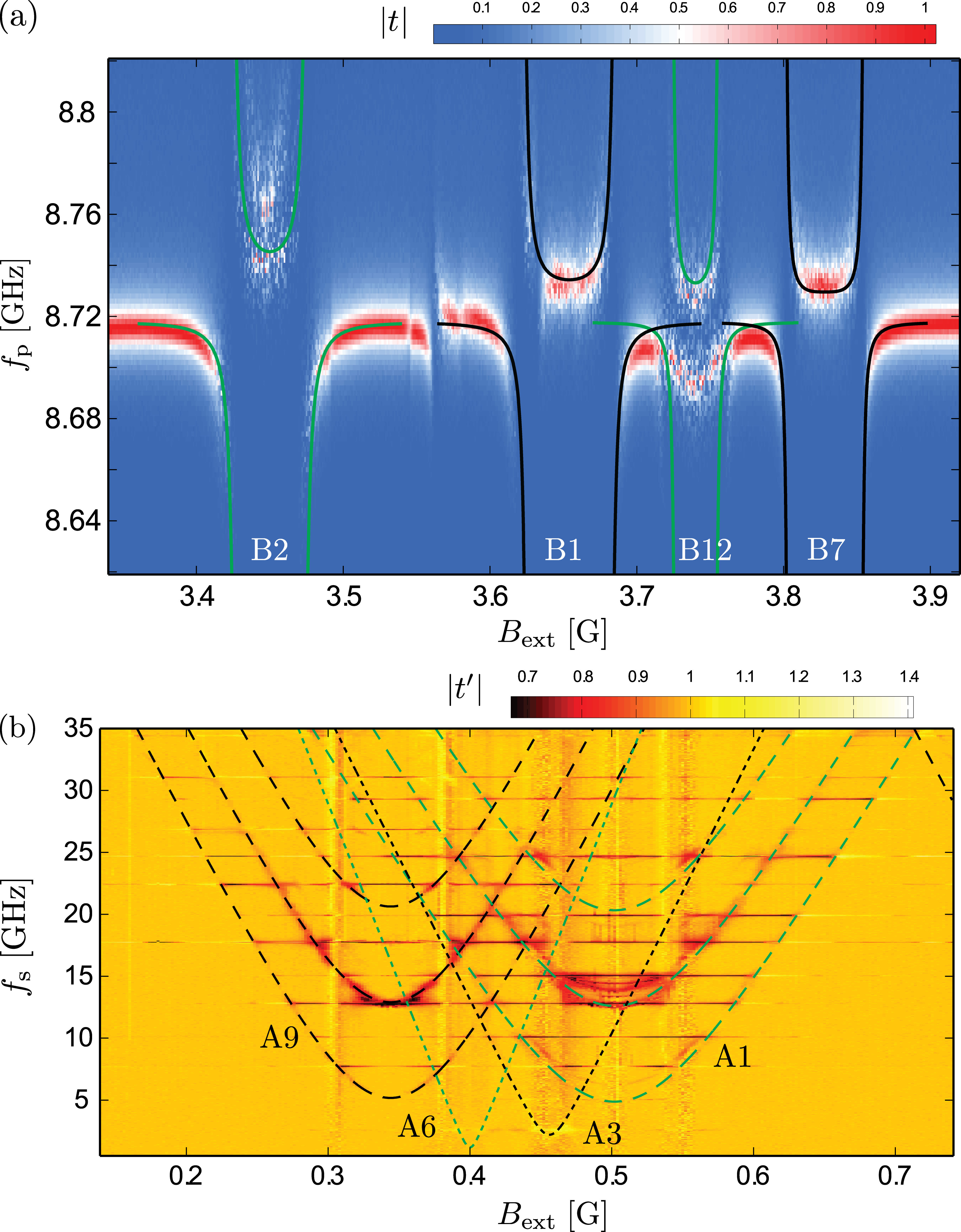
Transmission measurements. Figure 2 displays the result of the main qubit characterization measurement of sample B: in a range of around , and over a range of . Avoided crossings typical for coherently coupled qubit–resonator systems are observed, with corresponding features present also in (not shown). Measuring over a wider range of and extracting the periodicity in field of each feature in Fig. 2 allows us to identify the loop from which they originate. Our calculations agree reasonably with the measured transmission supplement . For 4 qubits, the lines in Fig. 2 show the two lowest transitions, calculated according to the Jaynes–Cummings model wallraff04 by considering at a time only a single qubit coupled to the resonator.
To determine and of the qubits (from the minimum value and slope of vs. , respectively), we perform two-tone spectroscopy by continuously monitoring transmission at the fixed frequency , while simultaneously sweeping the frequency of the additional spectroscopy tone over a wide range astafiev10 . The result for sample A over a short range of is shown Fig. 2 , including calculated for selected qubits. denotes the transmission amplitude normalized separately at each magnetic field by its value when is far detuned from any qubit or resonator transitions. The vertically offset curves with the same line type correspond to multiphoton processes with . In some cases, telegraph noise typical for two-level fluctuations is observed. We attribute this to background charge fluctuators affecting .
| Loop | 111Re-measurement of sample B after thermal cycling to | ||||
|---|---|---|---|---|---|
| A1 | 27.4 | 21.6 | 2.3 | 12.6 | |
| A2 | 26.8 | 20.2 | 2.6 | – | |
| A3 | 29.2 | 25.1 | 2.0 | 2.3 | |
| A4 | 30.0 | 24.9 | 2.2 | 1.0 | |
| A5 | 34.0 | 29.6 | 2.0 | – | |
| A6222Wire length by design ( for wires 1–5); normalized by 750/500 | 31.5 | 27.2 | 1.9 | 0.9 | |
| B1 | 28.0 | 22.2 | 2.4 | 7.0 | 7.0 |
| B2 | 29.6 | 23.2 | 3.0 | 7.3 | 5.5 |
| B3333 determined from -measurement to approximately accuracy (vs. with two-tone spectroscopy) | 29.0 | 24.1 | 1.7 | 1.4 | 0.9 |
| B4333 determined from -measurement to approximately accuracy (vs. with two-tone spectroscopy) | 29.1 | 24.8 | 2.2 | 0.8 | 1.0 |
| B5333 determined from -measurement to approximately accuracy (vs. with two-tone spectroscopy) | 30.7 | 26.8 | 1.9 | 1.6 | 2.5 |
| B6222Wire length by design ( for wires 1–5); normalized by 750/500333 determined from -measurement to approximately accuracy (vs. with two-tone spectroscopy) | 30.8 | 26.2 | 1.5 | – | 1.3 |
Analysis of the phase slip amplitude. Table 1 and Fig. 3 summarize the results. In Table 1 we collect the average wire widths , the minimum widths , and the width standard deviations , together with the experimentally derived and , the latter obtained after thermal cycling of sample B to . Figure 3 shows versus . For both samples, we focus on the qubits from loops 1–6 with wires of better quality (sample A: A1–A6 and B: B1–B6), featuring smallest relative roughness in width. During EBL, the nominally narrowest wires in these loops were written as single pixel lines, resulting in . In contrast, of the other detected qubits (from loops 7–12, patterned in area mode with sub-optimal dose, yielding ) do not follow any apparent dependence on , indicating that these wires behave as multiply constricted rather than uniform barriers for the flux tunneling. We take the SEM resolution into account in the wire width derivation, while additional unknown systematic error can remain in the absolute values of . Effective can also be reduced by a few nanometers due to oxidation at the edges. Nevertheless, it should not affect the overall dependence. Note that almost all wires 1–6 work as good tunnel barriers for the magnetic flux. However, signatures from loops A2 and A5 with minimal and maximal are not found. We suppose that this is due to too high (more than ) and too low (less than ) to be detected by our methods, consistent with our expectations.
We now compare the data with the theoretical expectations. As any quantum tunneling, the phase slip process is expected to be exponential in the tunnel barrier width:
| (1) |
where is related to an attempt frequency and gives the width at which the wire becomes essentially a one dimensional channel characterized by large quantum fluctuations. Qualitatively, the trend in Fig. 3 agrees with this exponential dependence. However, the –values exhibit large scatter. It can originate from small non-uniformities in material parameters or film thickness, or the remaining wire width roughness. In addition, because of the exponential dependence of the tunneling rate on the number of conduction channels , mesoscopic fluctuations of the conductance altshuler85 are expected to result in large fluctuations .
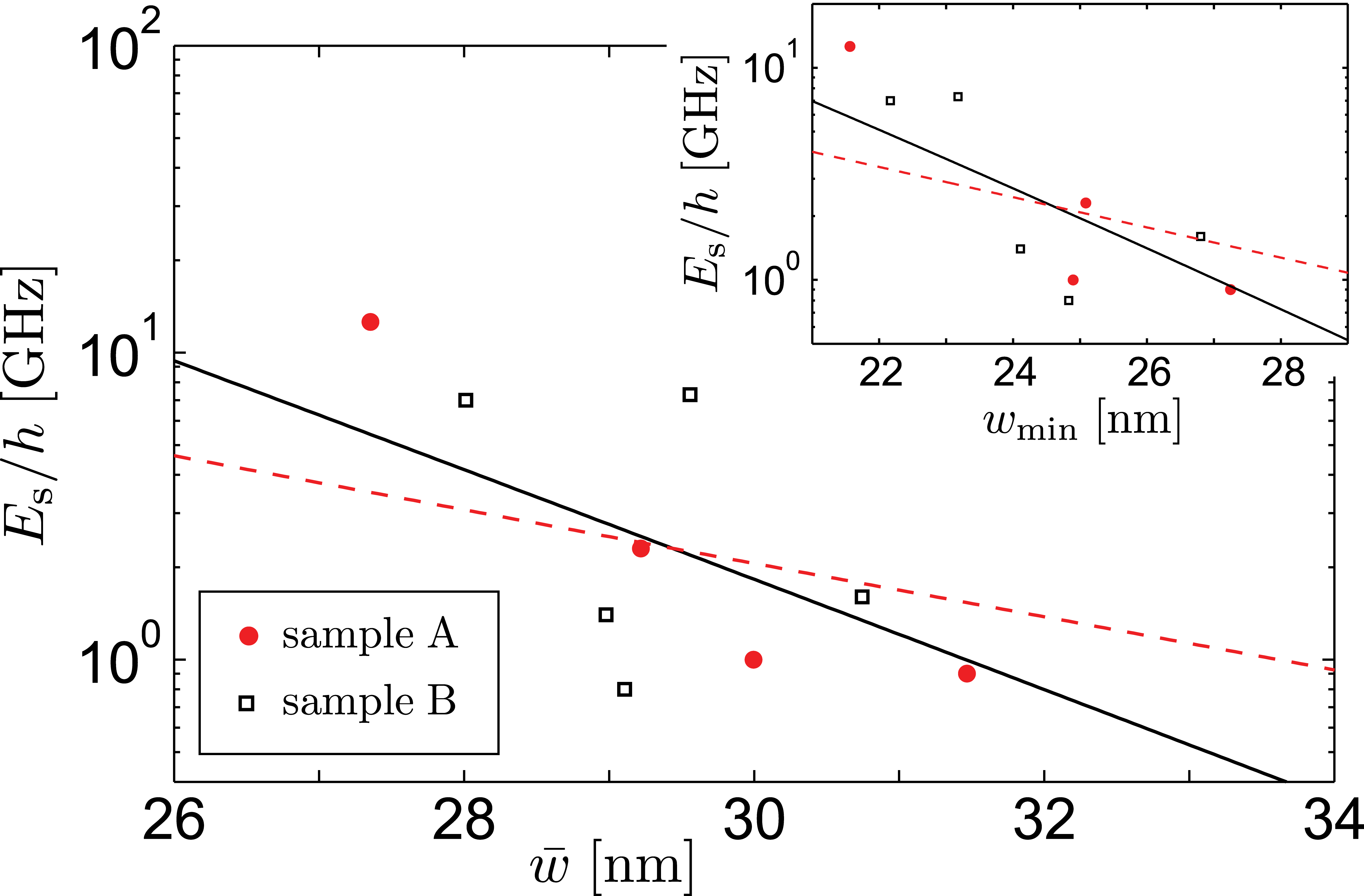
The BCS–based theory of QPS in moderately disordered superconductors zaikin97 ; golubev01 ; arutyunov08 gives the parameters in Eq. (1) for : and . Here, is the superconducting energy gap, the quantum resistance, the normal state sheet resistance of the film, the wire length, the superconducting coherence length, and denotes a dimensionless parameter of order unity. We use inferred from direct measurements of the gap in NbN films similar to those used here, known for thicker films bell07 , and the approximate low temperature resistance . A linear fit to yields the reasonable value (solid black line in Fig. 3), whereas the corresponding kinetic inductance expected from BCS theory deviates from the measured . Poor applicability of the BCS theory, however, is not surprising for the strongly disordered material, and not strictly one-dimensional wires. Here also random charge distribution along the wire is not accounted, which results in . Moreover, recent extension semenov13 of the microscopic model zaikin97 ; golubev01 indicates that interaction of individual phase-slip events can become relevant and affect the observable .
Now, we compute according to the phenomenological model ioffe10 ; feigelman10 of the strongly disordered superconductors, where the measured enters directly as an input parameter. In this model and , where is the superfluid stiffness , the numerical parameter , and is the Cooper pair density of states astafiev12 ; nupnote . Based on the diffusion coefficient of the films semenov01 we fix . A fit then yields the reasonable value (dashed red line in Fig. 3). Next, in the inset of Fig. 3 we show as a function of . Assuming that is dominated by the tunneling amplitude via a single constriction as suggested in Ref. vanevic12, , we approximate and obtain (solid line) or (dashed). Note that estimates using give the correct order of the without any fitting parameters.
Sample B was cooled down twice to study the effects of thermal cycling. As evident from Table 1, changes a little compared to the first measurement. This may be interpreted in terms of the Aharonov–Casher effect, i.e., interference of PS from different regions of the wire, and its dependence on the surrounding offset charges manucharyan12 ; pop12 . As argued in Ref. vanevic12, , the PS nature of the wires is retained even if they contain weak constriction-type inhomogeneities: The requirement is that the constriction resistance is much smaller than the total wire resistance, a condition likely satisfied by our wires.
Besides the initial demonstration of CQPS in wires and the NbN wires discussed in this Letter, we have recently observed qubit behavior in nanowires from ALD–grown TiN as well as purposely-made short constrictions in NbN and TiN. Similar to , the cause of strong decoherence in the nanowire qubits requires further study. For the fabrication of practical devices utilizing CQPS, the ideal would be a disordered material with highly reproducible fabrication process, together with minimized wire roughness. In conclusion, we find phase-slip flux qubit behavior with systematic wire-width dependence, in agreement with the theory of CQPS up to exponential accuracy.
Acknowledgements.
The work was financially supported by the JSPS FIRST program and MEXT Kakenhi ’Quantum Cybernetics’. We acknowledge financial support from the Ministry of Education and Science of the Russian Federation (Agreement No. 14B.37.21.1214 and contract No. 14.B25.31.0007). L. B. I. acknowledges financial support from ARO W911NF-09-1-0395, ANR QuDec and John Templeton Foundation, and T. M. K. from EU MicroKelvin (No. 228464, Capacities Specific Programme), the Dutch Foundation for Research of Matter (FOM), and Ministry of Education and Science of the Russian Federation under contract No. 14.B25.31.0007. We thank E. F. C. Driessen and P. J. C. C. Coumou for helpful comments.References
- (1) J. M. Martinis, M. H. Devoret, and J. Clarke, Phys. Rev. B 35, 4682 (1987).
- (2) J. Clarke and F. K. Wilhelm, Nature 453, 1031 (2008).
- (3) J. E. Mooij and Yu. V. Nazarov, Nature Phys. 2, 169 (2006).
- (4) W. A. Little, Phys. Rev. 156, 396 (1967).
- (5) M. Tinkham, Introduction to Superconductivity, 2nd ed. (McGraw-Hill, 1996).
- (6) K. Yu. Arutyunov, D. S. Golubev, and A. D. Zaikin, Phys. Rep. 464, 1 (2008).
- (7) N. Giordano, Phys. Rev. Lett. 61, 2137 (1988).
- (8) A. Bezryadin, C. N. Lau, and M. Tinkham, Nature 404, 971 (2000).
- (9) F. Altomare, A. M. Chang, M. R. Melloch, Yu. Hong, and C. W. Tu, Phys. Rev. Lett 97, 017001 (2006).
- (10) M. Zgirski, K.-P. Riikonen, V. Touboltsev, and K. Yu. Arutyunov, Phys. Rev. B 77, 054508 (2008).
- (11) O. V. Astafiev, L. B. Ioffe, S. Kafanov, Yu. A. Pashkin, K. Yu. Arutyunov, D. Shahar, O. Cohen, and J. S. Tsai, Nature 484, 355 (2012).
- (12) J. E. Mooij and C. J. P. M. Harmans, N. J. Phys. 7, 219 (2005).
- (13) Y. Nakamura, Yu. A. Pashkin, and J. S. Tsai, Nature 398, 786 (1999).
- (14) E. F. C. Driessen, P. C. J. J. Coumou, R. R. Tromp, P. J. de Visser, and T. M. Klapwijk, Phys. Rev. Lett. 109, 107003 (2012).
- (15) A. M. Hriscu and Yu. V. Nazarov, Phys. Rev. B 83, 174511 (2011).
- (16) A. J. Kerman, arXiv:1201.1859 (2012).
- (17) T. T. Hongisto and A. B. Zorin, Phys. Rev. Lett. 108, 097001 (2012).
- (18) J. S. Lehtinen, K. Zakharov, and K. Yu. Arutyunov, Phys. Rev. Lett. 109, 187001 (2012).
- (19) K. A. Matveev, A. I. Larkin, and L. I. Glazman, Phys. Rev. Lett. 89, 096802 (2002).
- (20) K. Yu. Arutyunov, T. T. Hongisto, J. S. Lehtinen, L. I. Leino, and A. L. Vasiliev, Sci. Rep. 2, 293 (2012).
- (21) We neglect the contribution of the geometric inductance, estimated as for our films.
- (22) A. Wallraff, D. I. Schuster, A. Blais, L. Frunzio, R.-S. Huang, J. Majer, S. Kumar, S. M. Girvin, and R. J. Schoelkopf, Nature 431, 162 (2004).
- (23) V. F. Gantmakher and V. T. Dolgopolov, Phys.-Usp. 53, 1 (2010).
- (24) A. D. Semenov, G. N. Gol’tsman, and A. A. Korneev, Physica C 351, 349 (2001).
- (25) B. Sacépé, C. Chapelier, T. I. Baturina, V. M. Vinokur, M. R. Baklanov, and M. Sanquer, Phys. Rev. Lett. 101, 157006 (2008).
- (26) B. Sacépé, C. Chapelier, T. I. Baturina, V. M. Vinokur, M. R. Baklanov, and M. Sanquer, Nature Commun. 1, 140 (2010).
- (27) B. Sacépé, T. Dubouchet, C. Chapelier, M. Sanquer, M. Ovadia, D. Shahar, M. V. Feigel’man, and L. B. Ioffe, Nature Phys. 7, 239 (2011).
- (28) Y. Noat, T. Cren, C. Brun, F. Debontridder, V. Cherkez, K. Ilin, M. Siegel, A. Semenov, H.-W. Hübers, and D. Roditchev, Phys. Rev. B 88, 014503 (2013).
- (29) See Supplemental Material for description of the sample fabrication process, resonator properties, and modeling of the microwave transmission.
- (30) O. V. Astafiev, A. A. Abdumalikov, Jr., A. M. Zagoskin, Yu. A. Pashkin, Y. Nakamura, and J. S. Tsai, Phys. Rev. Lett. 104, 183603 (2010).
- (31) B. L. Altshuler, JETP Lett. 41, 648 (1985).
- (32) A. D. Zaikin, D. S. Golubev, A. van Otterlo, and G. T. Zimanyi, Phys. Rev. Lett. 78, 1552 (1997).
- (33) D. S. Golubev and A. D. Zaikin, Phys. Rev. B 64, 014504 (2001).
- (34) M. Bell, A. Sergeev, V. Mitin, J. Bird, A. Verevkin, and G. Gol’tsman, Phys. Rev. B 76, 094521 (2007).
- (35) A. G. Semenov and A. D. Zaikin, Phys. Rev. B 88, 054505 (2013).
- (36) L. B. Ioffe and M. Mezard, Phys. Rev. Lett. 105, 037001 (2010).
- (37) M. V. Feigel’man, L. B. Ioffe, and M. Mezard, Phys. Rev. B 82, 184534 (2010).
- (38) is related to the density of states of electrons per unit area via .
- (39) M. Vanevic and Yu. V. Nazarov, Phys. Rev. Lett. 108, 187002 (2012).
- (40) V. E. Manucharyan, N. A. Masluk, A. Kamal, J. Koch, L. I. Glazman, and M. H. Devoret, Phys. Rev. B 85, 024521 (2012).
- (41) I. M. Pop, B. Doucot, L. Ioffe, I. Protopopov, F. Lecocq, I. Matei, O. Buisson, and W. Guichard, Phys. Rev. B 85, 094503 (2012).