Transformation Electromagnetics Devices Based on Printed-Circuit Tensor Impedance Surfaces
Abstract
A method for designing transformation electromagnetics devices using tensor impedance surfaces (TISs) is presented. The method is first applied to idealized tensor impedance boundary conditions (TIBCs), and later to printed-circuit tensor impedance surfaces (PCTISs). A PCTIS is a practical realization of a TIBC. It consists of a tensor impedance sheet, which models a subwavelength patterned metallic cladding, over a grounded dielectric substrate. The method outlined in this paper allows anisotropic TIBCs and PCTISs to be designed that support tangential wave vector distributions and power flow directions specified by a coordinate transformation. As an example, beam-shifting devices are designed, using TIBCs and PCTISs, that allow a surface wave to be shifted laterally. The designs are verified with a commercial full-wave electromagnetic solver. This work opens new opportunities for the design and implementation of anisotropic and inhomogeneous printed-circuit or graphene based surfaces that can guide or radiate electromagnetic fields.
Index Terms:
Anisotropic structures, artificial impedance surfaces, impedance sheets, metasurfaces, periodic structures, surface impedance, surface waves, tensor surfaces, transformation electromagneticsI Introduction
TRANSFORMATION electromagnetics was first introduced in 2006 [1]. Since that time, it has been applied to the design of novel microwave and optical devices such as cloaks, polarization splitters, and beam-benders [1, 2, 3]. Transformation electromagnetics allows a field distribution to be transformed from an initial configuration to a desired one via a change of material parameters dictated by coordinate transformation. In addition to volumetric designs, planar transformation-based devices using transmission-line networks have been recently introduced in [4], and subsequently pursued by other groups [5, 6, 7, 8, 9].
The need to integrate antennas and other electromagnetic devices onto the surfaces of vehicles and other platforms has driven interest in scalar, tensor, and periodic impedance surfaces in recent years. Planar leaky-wave antennas, based on scalar impedance surfaces, have been designed using sinusoidally modulated surface impedance profiles [10, 11] and tunable surface impedance profiles [12, 13, 14]. Great strides have been made in realizing practical printed devices such as holographic antennas, polarization controlling surfaces, and wave-guiding surfaces using the anisotropic properties of tensor impedance surfaces (TISs) [15, 16, 17, 18, 19, 20, 21]. In this paper, a method for designing transformation electromagnetics devices using TISs is presented.
We first present a method to implement transformation electromagnetics devices using an idealized tensor impedance boundary condition (TIBC) [22, 15]. Later in the paper, the method is adapted for printed-circuit tensor impedance surfaces (PCTISs), which are practical realizations of TIBCs [23, 24, 25, 26]. The TIBC is given by: , where and are components of the total electric and magnetic field tangential to the surface (at and is the surface normal[22]. This boundary condition can be represented in matrix form as
| (1) |
or in terms of the surface admittances as
| (2) |
where
| (3) |
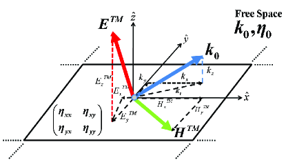
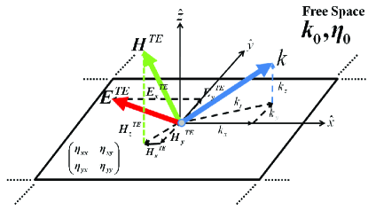
A TIS can support (Fig. 1(a)), (Fig. 1(b)), or hybrid modes. Recently, a surface impedance cloak was designed [27] using the index profile characteristic of a beam-shifter [28]. In the present work, the surface impedance profile needed to implement transformation electromagnetics devices is found from the transformed wave vector and Poynting vector distributions along a surface [29]. Specifically, surface impedance profiles are found that support modes (, , or hybrid) with these transformed phase and power characteristics. The method ensures that only the surface impedance entries need to be transformed, and the free space above the TIS need not be transformed. The method is later adapted to design practical PCTISs that also support modes with transformed wave vector and Poynting vector distributions. A PCTIS is a practical realization of a TIBC, consisting of a patterned metallic cladding over a grounded dielectric substrate. The patterned metallic cladding is modeled as a tensor sheet impedance [23, 24, 25, 26]. When designing PCTISs, the tensor sheet impedance entries are the unknowns: the quantities of interest.
In the next section of this paper, transformation electromagnetics in two dimensions (2D) is reviewed. Section III outlines an approach for designing 2D transformation electromagnetics devices using TIBCs. In Section IV, a beam-shifting device is designed and simulated with a commercial full-wave solver to verify the design method outlined in Section III. In Section V, transformation electromagnetics is applied to PCTISs, and a beam-shifter is designed using a PCTIS in Section VI. The proposed design methodology is a step towards the realization of practical, transformation electromagnetics devices using PCTISs [15, 23].
II Two-Dimensional Transformations
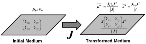
In transformation electromagnetics [1], fields are transformed from an initial state to a desired one via a change in material parameters based on a coordinate transformation. The transformed material tensors (and ) are related to the initial material parameters ( and ) in the following manner:
| (4) |
where
| (5) |
is the Jacobian of the transformation from the coordinate system to the system. When two-dimensional transformations are applied in the plane, the Jacobian reduces to
| (6) |
In transformation electromagnetics, material parameters transform as in (4). However, when designing TISs, the surface impedance/admittance is the quantity of interest rather than material parameters. Therefore, we must find how the surface admittance transforms. Transformation electromagnetics dictates that the transformed fields are related to the initial fields as [2, 30]:
| (7) |
| (8) |
or equivalently,
| (9) |
| (10) |
Rearranging the magnetic field components in (10), yields
| (11) |
Substituting (9) and (11) into the tensor admittance boundary condition (2) yields
| (12) |
Comparing equations (2) and (12) reveals that the transformation electromagnetics method transforms the surface admittance in the same manner that and are transformed in (4). That is,
| (13) |
The transverse resonance equation that determines the guided modes, for propagation along the -axis of an idealized TIBC [26] is given by
| (14) |
where , and . In general, the transverse wave number, , is given by but in this particular case, . The matrix on the right-hand-side (RHS) of (14) contains the and admittances of free space. Manipulating both sides of (14) yields
| (15) |
The term in square brackets on the LHS of (15) can be substituted with (12), yielding the following equation,
| (16) |
Therefore, not only is the surface admittance, , transformed but so is the free space above the surface (term in square brackets of (16)), to satisfy the guidance condition. This is impractical, since in many applications the space above the impedance surface is fixed: typically free space. This conclusion is verified through full-wave simulation in Section IV. The transformation of free space above the surface is not needed for two-dimensional transformation electromagnetics devices based on transmission lines [4, 5, 6, 7, 8, 9], since the fields are confined to the surface dimensions (i.e. ).
III Transformation Electromagnetics Applied to an Idealized Tensor Impedance Boundary Condition (TIBC)
In the previous section, it was shown that the transformed surface admittance () can be found from an initial surface impedance () in the same manner that the transformed material parameters are computed. However, to maintain the guidance condition, the free space above the surface must also be transformed. This section proposes an alternative design approach. In this alternative approach, tensor impedance entries ( and ) are found that support the spatially varying wave vector and Poynting vector of the transformation electromagnetics device, while maintaining free space above the surface.
A plane wave’s wave vector and Poynting vector tangential to the surface transform as [31]:
| (17) |
| (18) |
At a given spatial coordinate, the Poynting vector points at an angle, , with respect to the x-axis,
| (19) |
Similarly, the transformed wave vector points at an angle, with respect to the -axis. In addition to supporting the transformed wave vector and Poynting vector, the tensor impedance entries ( and ) must also satisfy the guidance condition for propagation along the surface.
III-A Propagation along TIBCs
The following eigenvalue equation ((17) in [23]) can be written to find the modes supported by a TIBC:
| (20) |
where
| (21) |
The eigenvalue equation above is found by expressing the tangential field components ( and ) in terms of the normal field components ( and ) corresponding to and fields, respectively [23, 32]. It should be noted that the double primes now denote field quantities corresponding to the transformed wave vector (17) and Poynting vector (18), not the transformed fields (given by (7) and (8)) from transformation electromagnetics. From (20), the dispersion equation of a TIBC can be derived [22, 23]:
| (22) |
The group velocity along a TIBC can be found by differentiating the dispersion equation (22) to find
| (23) |
The direction of power flow along a TIBC can then be expressed as [33]:
| (24) |
The eigenvalue equation (20) will be used to design TIBCs that support surface waves with the transformed wave vector and Poynting vector distributions given by (17) and (18).
III-B Design Approach
In transformation electromagnetics, the transformed material parameters are derived from an initial medium. This initial medium is typically free space. Since the intent here is to apply transformation electromagnetics to TIBCs, an initial isotropic surface impedance,
| (25) |
in free space is chosen that supports a surface wave at a desired frequency of operation. The surface impedance supporting a surface wave is given by
| (26) |
The tangential wave number () along the surface is chosen to be greater than that of free space to ensure a bound surface wave. Next, a surface impedance,
| (27) |
is found which supports the transformed wave vector and Poynting vector distributions on the surface. By writing the Poynting vector components in terms of and , (19) can be recast as
| (28) |
Therefore, the transformed wave vector and direction of the Poynting vector ()) along the surface, uniquely define the ratio of the normal electric to magnetic fields (ratio of to fields) supported by the TIBC. Even though the isotropic surface impedance supports a wave only, the anisotropic surface impedance can support a mixture of and waves, as indicated by (28). Equation (28) first appears in [29] but there, it contains a typographical error. Substituting (28) into (20) yields two (out of three) equations for finding the surface impedance entries: and . Setting the determinant of the transformed surface impedance tensor equal to the square of the initial surface impedance (), results in a third equation,
| (29) |
The transformed surface impedance entries can now be found using these three equations. This condition on the determinant of the surface impedance is analogous to the condition on the permittivity and permeability tensors in transformation electromagnetics devices [31]. Solving this system of three equations yields the surface impedance tensor necessary (at each point on the surface) to ensure the desired distributions of wave vector (17) and direction of power flow (18) along the surface. Alternatively, the system of three equations needed to find the surface impedance entries can be chosen as: the dispersion equation (22), the direction of power flow (24), and (29).
IV Example: A Beam-shifting Surface using a TIBC
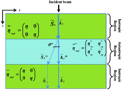
In this section, a transformation-based beam-shifter [34, 28] is designed using TIBCs. The device can bend a surface-wave beam by an angle of . The device consists of three regions (as shown in Fig. 3): an anisotropic region with surface impedance sandwiched between two isotropic regions with surface impedance . In the uppermost isotropic region, propagation is set to be purely in the -direction. The wave number is chosen to be rad/m at GHz, to ensure a tightly bound wave. The corresponding surface impedance is given by (26):
| (30) |
This surface will support a surface wave with the following propagation characteristics:
| (31) |
| (32) |
The anisotropic region is designed by finding the anisotropic surface impedance tensor () needed to bend the beam by an angle (Fig. 3). A coordinate transformation is applied to and to find the transformed tangential wave vector () and Poynting vector () in the anisotropic region. The Jacobian of the coordinate transformation governing the anisotropic region of the beam-shifting device is given by [2]
| (33) |
where The beam-shift angle is chosen to be or equivalently, . Applying the transformation to and , using (17) and (18) yields,
| (34) |
and
| (35) |
Applying the design procedure described in the previous section yields the following surface impedance tensor for the anisotropic region:
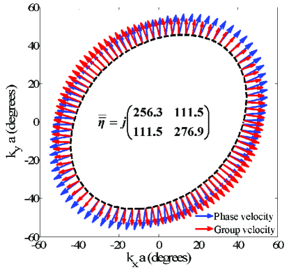
| (36) |
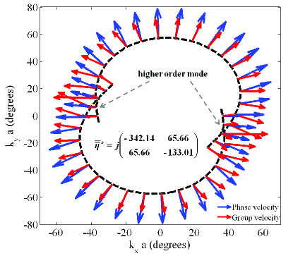
The dispersion contour for the anisotropic region is shown in Fig. 4.
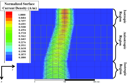
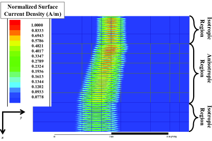
The beam-shifter was simulated using Ansys HFSS. The isotropic and anisotropic regions (as shown in Fig. 3) were modeled using the screening impedance boundary. The boundaries of the simulation domain were terminated with radiation boundaries, and one edge was illuminated with a Gaussian beam. The results of the simulation at 10 GHz are shown in Fig. 5. As expected, the Gaussian excitation couples energy into the uppermost isotropic surface, and a surface wave propagates in the -direction. Upon encountering the anisotropic region, the beam is refracted by . To an observer at the far edge of the lower isotropic region, (edge opposite the source), the source appears to have shifted laterally.
Had the surface admittance (30) been transformed by (12), the transformed surface impedance would be:
| (37) |
This surface impedance tensor does not satisfy the guidance condition at 10 GHz unless the free space above the surface is transformed to
| (38) |
| (39) |
via (4). This fact is verified using HFSS’s eigenmode solver. A unit cell of the TIBC given by (37) is implemented in HFSS with a screening impedance and the medium above the surface is assigned the anisotropic material parameters described by (38) and (39). When the phase delay corresponding to (34) is stipulated along the direction of the surface, an eigenfrequency of 10 GHz was found by the eigenmode solver. This verifies that for a surface transformed using (12), the guidance condition is only satisfied when the free space above the surface is also transformed. Additionally, finding the ratio of to from the simulation verifies the direction of power flow as When the free space above the surface is left untransformed in simulation, the guidance condition is satisfied at 9.874 GHz, which agrees with analytical predictions from the dispersion equation. At this frequency, the direction of power flow is
In the next section, a beam-shifter is implemented with a PCTIS. In the case of a PCTIS, the unknowns are the sheet admittance tensor entries (, , and ) rather than the surface admittance tensor entries.
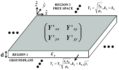
V Transformation Electromagnetics Applied to Printed-Circuit Tensor Impedance Surfaces (PCTISs)
In this section, a procedure for designing transformation electromagnetics devices using PCTISs is presented. A PCTIS consists of a tensor impedance sheet over a grounded dielectric substrate, where the tensor sheet impedance models a patterned metallic cladding. As shown in the analytical model of a PCTIS (see Fig. 6), the quantities of interest are the sheet admittance entries. The effective surface admittance of a PCTIS was related to the surface admittance of a TIBC in [26]. It was found that a PCTIS exhibits spatial dispersion due to its electrical thickness. As a result of this spatial dispersion, a PCTIS can have the same surface impedance as a TIBC, but a different direction of power flow [33]. The design method presented in the section is analogous to the design procedure for TIBCs from Section III. However, in the case of a PCTIS, one must find the sheet admittance entries (, , and ) that support the transformed wave vector and Poynting vector distributions of a transformation electromagnetics device.
V-A Propagation along PCTISs
The modes supported by a PCTIS can be found from eigenvalue equation (20) in [23]. The dispersion equation for a PCTIS can be derived from this eigenvalue equation as [23, 26],
| (40) |
Furthermore, the group velocity along a PCTIS was derived in [33] by differentiating the dispersion equation with respect to and . The and components of the group velocity along a PCTIS can be expressed compactly as:
| (41) |
where
| (42) |
and , , , and terms are given in Table III in Appendix B of [33]. The direction of power flow along a PCTIS is then given by
| (43) |
The dispersion equation (40) and the equation above (43) constitute two of the three equations needed to design a PCTIS that supports a surface wave with transformed wave vector and Poynting vector distributions. The third equation will be presented in the next subsection of this paper.
V-B Design Approach
Similar to the design approach for TIBCs outlined in Section III, an initial anisotropic medium must be stipulated. An isotropic sheet admittance,
| (44) |
is chosen to support a surface wave, with a desired transverse wave number, , at a chosen frequency of operation. For a surface wave, the isotropic sheet impedance is found from the transverse resonance equation [26]
| (45) |
or equivalently,
| (46) |
The transformed wave vector and Poynting vector are found from (17) and (18), respectively. Next, the sheet impedance tensor,
| (47) |
that supports the transformed wave vector and Poynting vector, is found by solving a system of three equations: the dispersion equation for a PCTIS (40), the expression for the direction of power flow along a PCTIS (43), and a condition on the determinant of the transformed sheet admittance [31],
| (48) |
Additionally, we must ensure that only a single mode is supported by the PCTIS. That is, the higher order mode should not be excited. The mode cutoff occurs when . At cutoff, the transverse resonance equation becomes
| (49) |
where is the sheet admittance at cutoff. The eigenvalues ( and ) of can be found by diagonalizing ,
| (50) |
where is a matrix containing the eigenvectors of . In order to ensure that the higher order mode is not excited, the eigenvalues ( and ) of must not exceed . When either of the eigenvalues is equal to , the mode can be excited. Beyond this resonance, the surface impedance is capacitive and a mode is supported in addition to the mode. In other words, the following conditions must be satisfied in order to guarantee only one mode exists:
| (51) |
and
| (52) |
where
| (53) |
| (54) |
Simultaneously solving the three aforementioned equations under the constraints of (51) and (52), the tensor sheet admittance entries (, , and ) can be found. The choice of the isotropic sheet () may have to be adjusted in order to satisfy (51) and (52) in addition to the three equations. Essentially, this condition places a limitation on the beam-shift angles achievable for a substrate with a given thickness and dielectric constant.
VI Example: A Beam-shifter using a PCTIS
In this section, a beam-shifter is designed using a PCTIS. The device can bend a surface-wave beam by at 10 GHz. It consists of three regions, as shown in Fig 3. The PCTIS beam-shifter consists of an isotropic sheet impedance in the upper and lower regions and an anisotropic sheet impedance in the middle. The sheets are on a 1.27 mm thick grounded dielectric substrate with =10.2. In the isotropic region, propagation is chosen to be in the -direction with a transverse wave number of rad/m. The isotropic sheet impedance, calculated using (44) and (46) is
| (55) |
The transformed wave and Poynting vectors are found to be
| (56) |
and
| (57) |
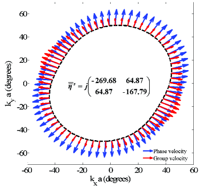
where . Solving the system of three equations ((40), (43), and (48)) discussed in the design procedure yields the following sheet impedance tensor for the anisotropic region:
| (58) |
The dispersion contour for this PCTIS is shown in Fig. 7.
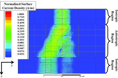
The beam-shifter was simulated using HFSS. The isotropic and anisotropic regions were modeled using the screening impedance boundary condition over a grounded dielectric substrate. The boundaries of the simulation domain were terminated with radiation boundaries, and one edge was illuminated with a Gaussian beam. The results of the simulation at 10 GHz are shown in Fig. 8. As expected, the Gaussian beam is refracted by upon encountering the anisotropic medium.
For the chosen substrate, S at 10 GHz. The eigenvalues (diagonalized sheet admittance values) of (58) are S and S, and therefore satisfy (51) and (52). If conditions (51) and (52) were not satisfied, a and a mode would co-exist. The 10 GHz dispersion contour for such a situation is shown in Fig. 9. The sheet impedance corresponding to this dispersion contour is
| (59) |
and the eigenvalues of are S and S. In this case, propagation along certain directions of the the beam-shifter will produce two beams. This is verified with full-wave simulation (results shown in Fig. 10) for propagation along the -axis.
VI-A Realization
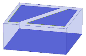
The PCTIS beam-shifter of Fig. 8 can be implemented by patterning the metallic cladding above a mm thick grounded dielectric substrate with . Using the sheet extraction method described in [23], a unit cell can be designed for the anisotropic region (see Fig. 11) that has a sheet impedance identical to that of (59). The isotropic region of the beam-shifter can be implemented by printing a square patch over the grounded dielectric substrate, similar to Fig. 11, but with the diagonal gap removed.
.
VII Conclusion
In this paper, a method for designing transformation electromagnetics devices using tensor impedance surfaces (TISs) was presented. It was shown that transforming an idealized tensor impedance boundary condition (TIBC) according to the transformation electromagnetics method, results in a transformation of the free space above it. An alternate method was proposed that allows transformation electromagnetics devices to be implemented using TIBCs, while maintaining free space above. The procedure was extended to include printed-circuit tensor impedance surfaces (PCTISs), which are practical realizations of TIBCs, and consist of a patterned metallic cladding over a grounded dielectric substrate. The alternate method allows anisotropic TIBCs and PCTISs to be designed that support tangential wave vector and Poynting vector distributions specified by a coordinate transformation. Beam-shifters are designed (both a TIBC and a PCTIS version) that laterally shift a surface wave beam at 10 GHz. The design methods reported in this paper may be applicable to graphene-based devices since an infinitesimally thin graphene sheet can be characterized by a conductivity tensor, using a non-local model for graphene [36]. Preliminary results of this work were presented at the 2013 IEEE International Microwave Symposium [29].
References
- [1] J. B. Pendry, D. Schurig, and D. R. Smith, “Controlling electromagnetic fields,” Science, vol. 312, pp. 1780–1782, Jun. 2006.
- [2] D.-H. Kwon and D. H. Werner, “Transformation electromagnetics: An overview of the theory and applications,” IEEE Antennas and Propagation Magazine, vol. 52, no. 1, pp. 24–46, Feb. 2010.
- [3] N. B. Kundtz, D. R. Smith, and J. B. Pendry, “Electromagnetic design with transformation optics,” Proceedings of the IEEE, vol. 99, no. 10, pp. 1622–1633, Oct. 2011.
- [4] G. Gok and A. Grbic, “Tensor transmission-line metamaterials,” IEEE Transactions on Antennas and Propagation, vol. 58, no. 5, pp. 1559 –1566, May 2010.
- [5] M. Zedler and G. V. Eleftheriades, “Anisotropic transmission-line metamaterials for 2-d transformation optics applications,” Proceedings of the IEEE, vol. 99, no. 10, pp. 1634–1645, Oct. 2011.
- [6] D.-H. Kwon and C. Emiroglu, “Non-orthogonal grids in two-dimensional transmission-line metamaterials,” IEEE Transactions on Antennas and Propagation, vol. 60, no. 9, pp. 4210–4218, Sept. 2012.
- [7] G. Liu, C. Li, C. Chen, Z. Lu, and G. Fang, “Experimental verification of field rotating with invisibility by full tensor transmission-line metamaterials,” Applied Physics Letters, vol. 101, no. 22, p. 224105, 2012.
- [8] M. Selvanayagam and G. Eleftheriades, “A sheared transmission-line metamaterial unit cell with a full material tensor,” in IEEE International Symposium on Antennas and Propagation, July, pp. 2872–2875.
- [9] M. Selvanayagam and G. Eleftheriades, “Transmission-line metamaterials on a skewed lattice for transformation electromagnetics,” IEEE Transactions on Microwave Theory and Techniques, vol. 59, no. 12, pp. 3272–3282, Dec. 2011.
- [10] A. M. Patel and A. Grbic, “A printed leaky-wave antenna with a sinusoidally modulated surface reactance,” in IEEE Antennas and Propagation Society International Symposium, Jun. 2009, pp. 1–4.
- [11] A. M. Patel and A. Grbic, “A printed leaky-wave antenna based on a sinusoidally-modulated reactance surface,” IEEE Transactions on Antennas and Propagation, vol. 59, no. 6, pp. 2087–2096, Jun. 2011.
- [12] D. F. Sievenpiper, “Forward and backward leaky wave radiation with large effective aperture from an electronically tunable textured surface,” IEEE Transactions on Antennas and Propagation, vol. 53, no. 1, pp. 236–247, Jan. 2005.
- [13] D. F. Sievenpiper, J. H. Schaffner, H. J. Song, R. Y. Loo, and G. Tangonan, “Two-dimensional beam steering using an electrically tunable impedance surface,” IEEE Transactions on Antennas and Propagation, vol. 51, no. 10, pp. 2713–2722, Oct. 2003.
- [14] D. F. Sievenpiper, J. Schaffner, J. J. Lee, and S. Livingston, “A steerable leaky-wave antenna using a tunable impedance ground plane,” IEEE Antennas and Wireless Propagation Letters, vol. 1, no. 1, pp. 179–182, 2002.
- [15] B. H. Fong, J. S. Colburn, J. J. Ottusch, J. L. Visher, and D. F. Sievenpiper, “Scalar and tensor holographic artificial impedance surfaces,” IEEE Transactions on Antennas and Propagation, vol. 58, no. 10, pp. 3212–3221, Oct. 2010.
- [16] B. H. Fong, J. S. Colburn, P. R. Herz, J. J. Oltusch, D. F. Sievepiper, and J. L. Visher, “Polarization controlling holographic artificial impedance surfaces,” in IEEE Antennas and Propagation Society International Symposium, Jun. 2007, pp. 3824–3827.
- [17] D. Sievenpiper, J. Colburn, B. Fong, J. Ottusch, and J. Visher, “Holographic artificial impedance surfaces for conformal antennas,” in IEEE Antennas and Propagation Society International Symposium, vol. 1B, Jul. 2005, pp. 256–259.
- [18] J. S. Colburn, D. F. Sievenpiper, B. H. Fong, J. J. Ottusch, J. L. Visher, and P. R. Herz, “Advances in artificial impedance surface conformal antennas,” in IEEE Antennas and Propagation Society International Symposium, Jun. 2007, pp. 3820–3823.
- [19] J. S. Colburn, A. Lai, D. F. Sievenpiper, A. Bekaryan, B. H. Fong, J. J. Ottusch, and P. Tulythan, “Adaptive artificial impedance surface conformal antennas,” in IEEE Antennas and Propagation Society International Symposium, Jun. 2009, pp. 1–4.
- [20] G. Minatti, F. Caminita, M. Casaletti, and S. Maci, “Leaky wave circularly polarized antennas based on surface impedance modulation,” in ICECom, 2010 Conference Proceedings, Sept. 2010, pp. 1–4.
- [21] D. J. Gregoire and A. V. Kabakian, “Surface-wave waveguides,” IEEE Antennas and Wireless Propagation Letters, vol. 10, pp. 1512–1515, 2011.
- [22] H. J. Bilow, “Guided waves on a planar tensor impedance surface,” IEEE Transactions on Antennas and Propagation, vol. 51, no. 10, pp. 2788–2792, Oct. 2003.
- [23] A. M. Patel and A. Grbic, “Modeling and analysis of printed-circuit tensor impedance surfaces,” IEEE Transactions on Antennas and Propagation, vol. 61, no. 1, pp. 211–220, Jan. 2013.
- [24] A. M. Patel and A. Grbic, “Analytical modeling of a printed-circuit tensor impedance surface,” in IEEE MTT-S International Microwave Symposium Digest, Jun. 2012, pp. 1–3.
- [25] A. M. Patel and A. Grbic, “Dispersion analysis of printed-circuit tensor impedance surfaces,” in IEEE Antennas and Propagation Society International Symposium, Jul. 2012, pp. 1–2.
- [26] A. M. Patel and A. Grbic, “Effective surface impedance of a printed-circuit tensor impedance surface (pctis),” IEEE Transactions on Microwave Theory and Techniques, vol. 61, no. 4, pp. 1403–1413, Apr. 2013.
- [27] R. Quarfoth and D. Sievenpiper, “Anisotropic surface impedance cloak,” in IEEE Antennas and Propagation Society International Symposium, Jul. 2012, pp. 1–2.
- [28] M. Y. Wang, J. J. Zhang, H. Chen, Y. Luo, S. Xi, L. X. Ran, and J. A. Kong, “Design and application of a beam shifter by transformation media,” Progress In Electromagnetics Research, vol. 83, pp. 147–155, 2008.
- [29] A. M. Patel and A. Grbic, “Transformation electromagnetics devices using tensor impedance surfaces,” in IEEE MTT-S International Microwave Symposium Digest, Jun. 2013.
- [30] B. Kuprel and A. Grbic, “Anisotropic inhomogeneous metamaterials using nonuniform transmission-line grids aligned with the principal axes,” IEEE Antennas and Wireless Propagation Letters, vol. 11, pp. 358–361, 2012.
- [31] G. Gok and A. Grbic, “Alternative material parameters for transformation electromagnetics designs,” IEEE Transactions on Microwave Theory and Techniques, vol. 61, no. 4, pp. 1414–1424, Apr. 2013.
- [32] J. A. Kong, Electromagnetic Wave Theory. Cambridge, MA: EMW Publishing, 2008.
- [33] A. M. Patel and A. Grbic, “The effects of spatial dispersion on power flow along a printed-circuit tensor impedance surface,” IEEE Transactions on Antennas and Propagation, Submitted Apr. 2013.
- [34] G. Gok and A. Grbic, “A printed beam-shifting slab designed using tensor transmission-line metamaterials,” IEEE Transactions on Antennas and Propagation, vol. 61, no. 2, pp. 728–734, Feb.
- [35] G. Minatti, S. Maci, P. De Vita, A. Freni, and M. Sabbadini, “A circularly-polarized isoflux antenna based on anisotropic metasurface,” IEEE Transactions on Antennas and Propagation, vol. 60, no. 11, pp. 4998–5009, Nov. 2012.
- [36] G. Hanson, “Dyadic green’s functions for an anisotropic, non-local model of biased graphene,” IEEE Transactions on Antennas and Propagation, vol. 56, no. 3, pp. 747–757, Mar. 2008.