Present address: ]School of Materials Science and Technology, Indian Institute of Technology (BHU), Varanasi-221005, India
Temperature dependence of Andreev spectra in a superconducting carbon nanotube quantum dot
Abstract
Tunneling spectroscopy of a Nb coupled carbon nanotube quantum dot reveals the formation of pairs of Andreev bound states (ABS) within the superconducting gap. A weak replica of the lower ABS is found, which is generated by quasi-particle tunnelling from the ABS to the Al tunnel probe. An inversion of the ABS-dispersion is observed at elevated temperatures, which signals the thermal occupation of the upper ABS. Our experimental findings are well supported by model calculations based on the superconducting Anderson model.
pacs:
73.63.Fg, 74.45.+c, 73.23.HkI Introduction
The proximity effect in a superconductor coupled to a mesoscopic normal conductor leads to a wide range of new quantum phenomena. These include Andreev reflection at normal and superconductor interfaces, the formation of Andreev bound states (ABS) in confined geometries, and proximity-induced supercurrent flow through normal conductors.Likharev79 ; Doh05 ; Jarillo06 ; nanosquid ; Pallecchi08 The recent experimental detection of individual Andreev bound statesPillet10 ; Dirks11 as well as the efforts towards demonstrating Majorana states in superconductor coupled nanostructures devices with strong spin-orbit interactionMourik12 received significant experimental and theoretical interest and opened a new area of research.
Quantum dots (QDs) coupled to superconducting leads provide an ideal system to test the theoretical predictions on the interplay of ABS with the Kondo effect.Kim13 A 0 to junction transitionMartin11 has been reported in S-QD-S systems by measuring the sign reversal (positive to negative) of the Josephson supercurrent for even to odd occupation of the QD.Franceschi10 ; Maurand12 ; Dam06 Theoretical calculations suggest that this quantum phase transition in the S-QD-S Josephson junction devices is signaled also by the crossing of two Andreev levels.Vecino03 ; Lim08 Depending on the ratio of the Kondo temperature at the center of a Coulomb valley and the superconducting gap energy , the ABS display a crossing () or a non-crossing () dispersion as a function of gate voltage . These predictions have been confirmed by recent experimental studies using Al-contacted semiconductor quantum dot / nanowire devices.Kim13 ; Deacon10 ; Chang12 ; Lee13
It has also been predicted theoretically that there could be up to four ABS for a single level model in the superconducting gap. However the two outer ABS may not be visible in the transport spectrum since they can merge with the continuum.Vecino03 ; Martin12 ; Yoshioka00 ; Meng09 So far most of the experimental studies of ABS formation are limited to Al as contacts material, which restricts these experiments to very low temperatures and magnetic fields. Despite these earlier reports, the study of hybrid nanostructures with larger gap superconducting elements is required to allow for a more complete understanding of ABS formation in these devices.
Here, we report on low temperature tunnelling spectroscopy measurements on an individual carbon nanotube quantum dot device strongly coupled to a Nb superconducting loop and weakly coupled to an Al tunnel probe. Two types of ABS are observed in Coulomb valleys with different charging energy. In some gate regimes two pairs of ABS are found within the superconducting gap. In addition, next to the main ABS conductance resonance a weaker conductance peak is present, which is interpreted as quasi-particle tunnelling from the ABS to the Al tunnel probe. At higher temperatures tunneling from the thermally populated upper ABS becomes visible and shows an opposite curvature at the center of the Coulomb valleys. Calculations based on the superconducting Anderson model are used to describe the experimentally observed subgap features.
II Experimental details
Single wall CNTs are grown on a Si/SiO2 substrate by chemical vapor deposition using a Fe/Mo based catalyst and methane as precursor gas. The highly doped Si substrate with 300 nm SiO2 layer serves as a global back gate.
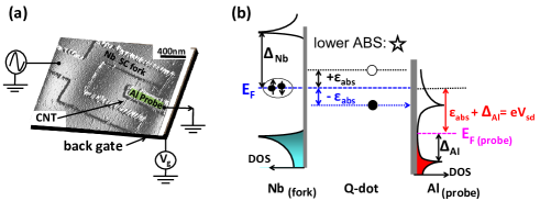
A niobium ( Pd / Nb) superconducting loop and a tunnel probe ( Ti / Al) are patterned using standard electron beam lithography on an individual single wall carbon nanotube (Figure 1(a)). A Pd interlayer is used to improve the coupling between the superconducting fork and the nanotube and thereby increase the superconducting proximity effect. For weak coupling of the tunnel probe to the CNT a thin Ti adhesion layer is used. Low temperature electrical transport measurements are performed in a 3He/4He dilution refrigerator with heavily filtered signal lines down to . The differential conductance of the superconducting tunnel probe weakly connected to the nanotube was measured employing conventional lock-in techniques by adding a low frequency ac excitation voltage (, ) onto the dc bias voltage . Variation of the back gate voltage gives access to the ABS spectrum in the CNT-QD.
The device parameters are extracted by measurements in both the superconducting and the normal conducting state (by applying a magnetic field) of the contacts.
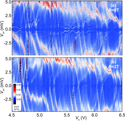
Corresponding overview plots of the differential conductance are shown in Fig. 2. While in Fig. 2(a) at zero applied magnetic field features pertaining to superconductivity in the leads dominate transport at low bias, a magnetic field of restores the typical pattern of Coulomb blockade in Fig. 2(b). The superconducting gap of the Nb loop is found to be , and for the Al tunnel probe and are estimated. Typical parameter values of the CNT-QD are the charging energy , the tunnel coupling to the leads , and the coefficient which relates the energies of the quantum dot states to .
III Andreev Bound State features
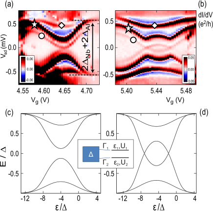
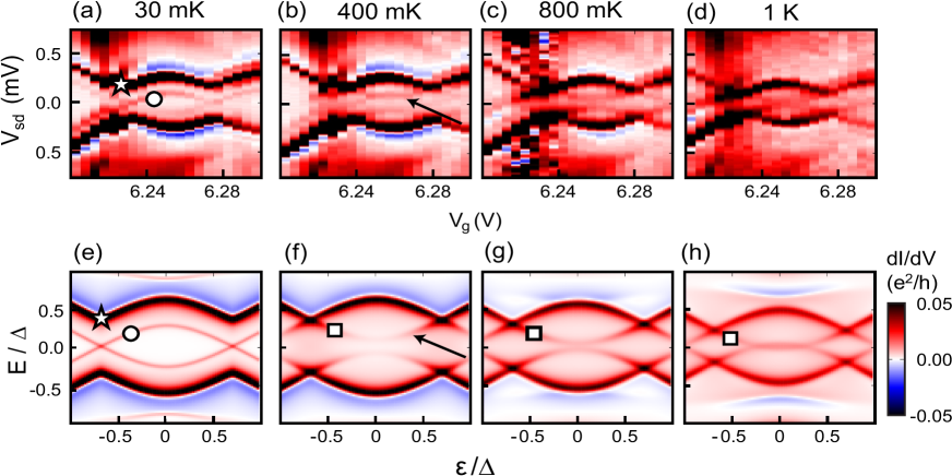
Figure 3 shows two details of the stability diagram, where the differential conductance is again plotted as a function of bias and gate voltage , at base temperature and zero magnetic field. The two panels (a) and (b) correspond to two different gate voltage ranges exhibiting different charging energies and , respectively. Within the superconducting gap range there are three subgap features: two main resonances of high conductance (, ), and a weak conductance resonance () running parallel to the resonance (). Strong peaks in the differential conductance measurements are expected when an Andreev level at is aligned to the BCS singularity of the density of states of the tunnel probe (see figure 1(b)). This results in pronounced conductance peaks at voltages .Pillet10 The weak conductance peak () running parallel to the lower ABS () at lower bias voltages is understood as a replica of the ABS at low temperatures (see below).
As already mentioned the ABS () spectrum for odd charge states can show non-crossing (Fig. 3(a)) or crossing behavior of the pairs of bound states (Fig. 3(b)), resulting in a 0- quantum phase transition.Deacon10 ; Kim13 This is controlled by the ratio .Kim13 ; Deacon10 ; Chang12 ; Pillet13 ; Futterers13 In case of non-crossing the system always stays in the 0-phase, i.e. a (singlet) ground state whereas for a zero bias crossing of the ABS the system changes its ground state from 0 to -state (magnetic doublet).
Fig. 3(c) and (d) show the ABS spectrum obtained from the superconducting Anderson model using the numerical renormalization group (NRG) method.Yoshioka00 ; Martin12 We have found that the presence of two pairs of ABS can be explained by assuming the presence of two nearly degenerate levels, e.g., resulting from the often lifted KK’-symmetry that are coupled to two independent channels in the leads, as schematically drawn in the inset of the figure. For the case of Fig. 3(a) both channels are in the 0-phase and the ABS exhibit a non-crossing behavior as correspondingly shown in Fig. 3(c). On the other hand, in the case of Fig. 3(b) the inner ABS exhibit a loop indicating the transition to the -phase, which is accounted for in the theoretical result of Fig. 3(d) by a larger ratio for one of the channels. The values were taken as 8 (Fig. 3(c)) and 9 (Fig. 3(d)) close to the experimental estimations while the parameters were chosen to get a qualitative fit of the experimental results.
IV Temperature dependence
To understand the origin of the weak replicas of the inner pair of ABS in our experiment, we investigate their dependence on temperature. Figure 4(a–d) shows a detail of the 2D stability diagram in a different Coulomb valley at the indicated temperatures. In this gate regime, again a weak conductance resonance () running parallel to a pair of ABS () is observed. The apparent replica of the ABS can be understood if we assume that the probe DOS is finite at the Fermi energy and is aligned with the ABS: .
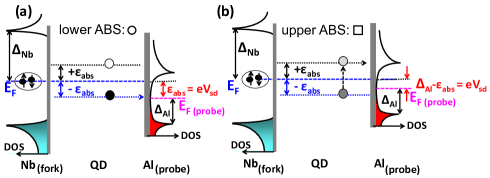
This level arrangement illustrated in Fig. 5(a). For a non-superconducting tunnel probe one would expect the disappearance of the replicas together with a shift in the main ABS due to the suppression of the probe gap . We have verified this by applying a small magnetic field () that drives the Al tunnel probe into the normal state: it suppresses the replica and a clear crossing of the main ABS () is then present (data not shown).
The main ABS peak () remains unchanged up to the maximum temperature investigated in the present study. The satellite peaks () also do not show any significant change up to . At , however, the dispersion of the gate voltage dependence of the satellite peaks flattens at the center of CB valley and an additional conductance resonance starts to emanate from the main ABS resonance (see the arrow in Fig. 4(b)). At even higher temperatures , the gate voltage dependence of the satellite peak changes its curvature at the center of the Coulomb valley compared to the low temperature () case.
As illustrated in the schematic of Fig. 5(b), we expect a peak in differential conductance when the maximum of the BCS density of states of the tunnel probe is aligned with the thermally populated upper state. The position of the secondary peak () should then be inverted, and vary as ). At intermediate temperatures () we observe that quasi particle tunnelling via both the lower and the thermally populated upper ABS (Fig. 4(b)) contributes to the current. The combined contributions lead to a nearly flat dispersion of the secondary peak. At higher temperatures (Fig. 4(c,d)) transport of thermally excited quasi-particles via the upper ABS dominates, which leads to the opposite curvature of the dispersion in the center of the Coulomb valley. The slight shift of both the ABS and their replica towards smaller energies results from the reduction of as the temperature is increased.
According to our model, the dispersion of all three types of conductance peak originates from the same dispersion relation . Hence, it should be possible to collapse the dispersion of the ABS and its replicas at low and high temperature on top of each other by suitable inversions and shifts.
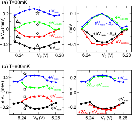
This is illustrated in Fig. 6, confirming our interpretation: At low temperature , Fig. 6(a) left panel, we observe in the differential conductance measurement the main ABS at and a satellite peak at . After subtracting the SC gap of the tunnel probe () at , the peak position of the main ABS peaks show a good overlap with the satellite peak (Fig. 6(a), right panel). At higher temperature , as depicted in Fig. 6(b) left panel, the dispersion of the satellite peak is inverted. Its position follows a relation with gate voltage in the Coulomb blockade valley. To verify this gate dependence, we compute and plot for a reduced , and find a very good match with the observed main peak position , see Fig. 6(b) right panel. A similar analysis for other temperatures also shows an excellent agreement with the proposed mechanism.
V Superconducting Anderson model
In addition to the measurement results, calculated conductance patterns for a quantum dot structure as described here are shown in Fig. 4(e)-(h). The conductance calculations were performed using a mean field description of the superconducting Anderson model coupled to two superconducting leads with two different gap parameters and . As discussed in Ref. Vecino03, the magnetic phase can be represented within a mean field description by introducing an exchange parameter which produces a splitting of the dot energy levels for different spin orientations. In these calculations the coupling to the Nb superconducting leads is included nonperturbatively (i.e. to all orders in perturbation theory) while the coupling to the Al probe is introduced to the lowest order in perturbation theory. This approximation is justified by the weak coupling strength to the probe electrode, manifested by the small conductance values experimentally observed (of the order of ). More precisely the conductance was calculated using
where are the local densities of states at the probe electrode and at the dot coupled to the Nb leads, respectively, is the Fermi distribution function and is the tunneling rate from the dot to the probe electrode. While is calculated using the mean field approximation for the Anderson model coupled to the Nb superconducting lead as described in Ref. Vecino03, , for we use a standard BCS-like density of states in which we introduce a phenomenological Dynes-parameterDynes of broadening the BCS density of states for the Al probe.
As can be observed in Fig. 4, the model calculations give a good description of the evolution of the weak subgap features with temperature, and once more confirm our interpretation in terms of different transport mechanisms. It should be noted that the only change in the model parameters when going from Fig. 4(e) to Fig. 4(h) is due to the reduction of with temperature, while we assume in this temperature range. The comparatively high value of the Dynes-parameter is at present not understood. This may be an effect of the electromagnetic environment,pekola2010 to which superconducting quantum dot devices are known to be extraordinarily sensitive.
VI Multi-loop structures and negative differential conductance
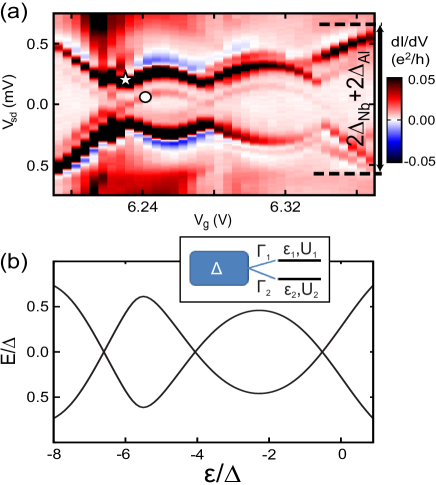
A peculiar feature of the present experimental results are the multiple loop ABS that are observed in a more extended gate range, as depicted in Fig. 7. As opposed to the situation considered in Fig. 3(c) and (d), a theoretical description of such multi-loop features is obtained when more than one dot level couples to the same channel in the leads, see the inset of Fig. 7(b). A NRG calculation considering such a situation with two hybridized levels on one dot can actually reproduce qualitatively the observed multi-loop patterns, as shown in Fig. 7(b).
In several of the Coulomb valleys investigated in more detail the ABS-peaks are accompanied by a pronounced negative differential conductance (NDC), shown in blue color in Figs. 3, 4, and 7. NDC features have been predicted to appear due to the presence of the so-called Yu-Shiba-Rusinov (YSR) states for a QD with an odd number of electronsAndersen11 with highly asymmetric coupling to the leads. YSR-states can be regarded as a variant of ABS appearing for a magnetic impurity coupled to a superconductor,Shiba68 and their existence has been experimentally confirmed via scanning tunneling microscopy of magnetic atoms on superconducting surfacesYazdani97 and QDs with superconducting leads.Kim13 ; Andersen11 ; Lee12 ; Yeyati97
VII Conclusions
In conclusion, our transport spectroscopy of an individual carbon nanotube strongly coupled to wide gap Nb leads reveals several different types of Andreev bound state spectra. Weak satellite peaks appear within the smaller probe superconducting gap which are a result of quasiparticle tunneling into a residual density of states within this gap. At higher temperature these satellite peaks change their dispersion as a function of gate voltage due to the thermal population of the upper state of an ABS pair. Our findings are well reproduced within the superconducting Anderson model in terms of combined NRG and mean field calculations. More efforts in this direction could be helpful also to discriminate Majorana bound states in similar hybrid nanostructures from other states at zero energy.
We gratefully acknowledge financial support from the Deutsche Forschungsgemeinschaft within GRK 1570, SFB 689, the E. Noether program (Hu 1808-1), from Spanish MINECO through grant FIS2011-26516, and from the EU FP7 Project SE2ND. A. K. thanks the Alexander von Humboldt Foundation for providing financial support during this research. We thank Kicheon Kang for enlightening discussions.
References
- (1) K. K. Likharev, Rev. Mod. Phys. 51, 101 (1979).
- (2) Y.-J. Doh, J. A. van Dam, A. L. Roest, E. P. A. M. Bakkers, L. P. Kouwenhoven, and S. De Franceschi, Science 309, 272 (2005).
- (3) P. Jarillo-Herrero, J. A. van Dam, and L. P. Kouwenhoven, Nature 439, 953 (2006).
- (4) J.-P. Cleuziou, W. Wernsdorfer, V. Bouchiat, T. Ondarcuhu, and M. Monthioux, Nature Nanotechnology 1, 53 (2006).
- (5) E. Pallecchi, M. Gaass, D. A. Ryndyk, and C. Strunk, Appl. Phys. Lett. 93, 072501 (2008).
- (6) J.-D. Pillet, C. H. L. Quay, P. Morfin, C. Bena, A. Levy-Yeyati, and P. Joyez, Nat. Phys. 6, 965 (2010).
- (7) T. Dirks, T. L. Hughes, S. Lal, B. Uchoa, Y. Chen, C. Chialvo, P. M. Goldbart, and N. Mason, Nature Physics 7, 386, (2011).
- (8) V. Mourik, K. Zuo, S. M. Frolov, S. R. Plissard, E. P. A. M. Bakkers, and L. P. Kouwenhoven, Science 336, 1003 (2012).
- (9) A. Martin-Rodero and A. Levy-Yeyati, Adv. Phys. 60, 899 (2011).
- (10) S. De Franceschi, L. P. Kouwenhoven, C. Schönenberger, and W. Wernsdorfer, Nature Nanotechnology 5, 703 (2010).
- (11) B.-K. Kim, Y.-H. Ahn, J.-J. Kim, M.-S. Choi, M.-H. Bae, K. Kang, J. S. Lim, R. Lopez, and N. Kim, Phys. Rev. Lett. 110, 076803 (2013).
- (12) R. Maurand, T. Meng, E. Bonet, S. Florens, L. Marty, and W. Wernsdorfer, Phys. Rev. X 2, 011009 (2012).
- (13) J. A. van Dam, Y. V. Nazarov, E. P. A. M. Bakkers, S. De Franceschi, and L. P. Kouwenhoven, Nature (London) 442, 667 (2006).
- (14) E. Vecino, A. Martin-Rodero, and A. Levy Yeyati, Phys. Rev. B 68, 035105 (2003).
- (15) J. S. Lim and M.-S. Choi, J. Phys. Condens. Matter 20, 415225 (2008).
- (16) R. S. Deacon, Y. Tanaka, A. Oiwa, R. Sakano, K. Yoshida, K. Shibata, K. Hirakawa, and S. Tarucha, Phys. Rev. Lett. 104, 076805 (2010); Phys. Rev. B 81, 121308(R) (2010).
- (17) W. Chang, V. E. Manucharyan, T. S. Jespersen, J. Nygard, and C. M. Marcus, Phys. Rev. Lett. 110, 217005 (2013).
- (18) E. J. H. Lee, X. Jiang, M. Houzet, R. Aguado, C. M. Lieber, and S. De Franceschi, arXiv:1302.2611 (2013).
- (19) A. Martin-Rodero and A. Levy-Yeyati, J. Phys. 24, 415301 (2012).
- (20) T. Yoshioka and Y. Ohashi, J. Phys. Soc. Jpn. 69, 1812 (2000).
- (21) T. Meng, S. Florens, and P. Simon, Phys. Rev. B 79, 224521 (2009).
- (22) J.-D. Pillet, P. Joyez, R. Zitko, and M. F. Goffman, Phys. Rev. B 88, 045101 (2013).
- (23) D. Futterer, J. Swiebodzinski, M. Governale, and J. König, Phys. Rev. B 87, 014509 (2013).
- (24) R. C. Dynes, V. Narayanamurti, and J. P. Garno, Phys. Rev. Lett. 41, 1509 (1978).
- (25) J. P. Pekola, V. F. Maisi, S. Kafanov, N. Chekurov, A. Kemppinen, Yu. A. Pashkin, O.-P. Saira, M. Möttönen, and J. S. Tsai, Phys. Rev. Lett. 105, 026803 (2010).
- (26) B. M. Andersen, K. Flensberg, V. Koerting, and J. Paaske, Phys. Rev. Lett. 107, 256802 (2011).
- (27) H. Shiba, Prog. Theor. Phys. 40, 435 (1968).
- (28) A. Yazdani, B. A. Jones, C. P. Lutz, M. F. Crommie, and D. M. Eigler, Science 275, 1767 (1997).
- (29) E. J. H. Lee, X. Jiang, R. Aguado, G. Katsaros, C. M. Lieber, and S. De Franceschi, Phys. Rev. Lett. 109, 186802 (2012).
- (30) A. Levy Yeyati, J. C. Cuevas, A. Lopez-Davalos, and A. Martin-Rodero, Phys. Rev. B 55, 6137 (1997).