A facile process for soak-and-peel delamination of CVD graphene from substrates using water
Abstract
We demonstrate a simple technique to transfer CVD-grown graphene from copper and platinum substrates using a soak-and-peel delamination technique utilizing only hot deionized water. The lack of chemical etchants results in cleaner CVD graphene films minimizing unintentional doping, as confirmed by Raman and electrical measurements. The process allows the reuse of substrates and hence can enable the use of oriented substrates for growth of higher quality graphene, and is an inherently inexpensive and scalable process for large-area production.
Graphene, a monolayer honeycomb lattice structure of sp2-bonded carbon atoms, has become a subject of great interest due to its extraordinary optical, mechanical, and electronic properties Geim and Novoselov (2007); Castro Neto et al. (2009); Novoselov et al. (2012). Successful isolation of graphene by the mechanical exfoliation of highly oriented pyrolytic graphite (HOPG) has opened doors for new innovations in the field of nanoelectronics Novoselov et al. (2004); Zhang et al. (2005). Since then many new methods have emerged to synthesize and isolate single to few-layer graphene Novoselov et al. (2012) especially on large area substrates. These methods include reduction of graphite oxide Stankovich et al. (2007), ultrasonication of graphite Hernandez et al. (2008), synthesis on SiC substrate Berger et al. (2004), and chemical vapor deposition (CVD) on metal substrates such as Ni Yu et al. (2008), Cu Li et al. (2009a), Ru Sutter, Flege, and Sutter (2008) and Pt Kang et al. (2009); Sutter, Sadowski, and Sutter (2009).
Of all these methods, the low-pressure growth of graphene on Cu foils, in particular, is known to be advantageous in terms of controlled graphene size, number of layers and quality Li et al. (2009a). It has also been shown that better quality graphene can be grown on Cu(111) oriented grains Wood et al. (2011). Thus CVD graphene growth on Cu produces large areas of mostly monolayer graphene and is a promising way of producing large area graphene for practical nanoelectronics applications Geim (2009); Novoselov et al. (2012). To fully realize the advantages of the CVD graphene growth there must be a reliable method for transferring the graphene from metallic Cu substrates to more useful substrates like insulating substrates Reina et al. (2009), flexible/stretchable substrates Kim et al. (2009), and transparent electrodes Bonaccorso et al. (2010); Bae et al. (2010). Pt(111), as a substrate for CVD graphene growth, is also interesting because it has minimum effect on the physical properties of graphene due to its very weak graphene-substrate interaction. Further, it has been shown that the electronic structure of the graphene grown on Pt is nearly the same as that of the free standing graphene Gao et al. (2011). In addition, Pt does not get oxidized easily like other metal substrates such as Cu.
Currently the processes used to transfer large-area and high-quality graphene synthesized on metal substrates require wet etching of the metal substrates Li et al. (2009a, b). These processes trap ionic species between graphene and substrate interface which act as scattering centers and lead to degradation of the electrical properties of the devices fabricated on the graphene. Further, the etching process also results in loss of metal ultimately increasing the cost of the transfer process; this is especially true for precious metals and oriented single crystal substrates that are expensive. Electrochemical methods to transfer graphene without metal loss have been demonstrated but they involve chemicals like NaOH and are complex Wang et al. (2011); Gao et al. (2012). An intercalation method to transfer graphene from Pt to other substrates has also been shown, but for small size graphene flakes only Ma et al. (2013). To overcome these problems, we demonstrate, a novel facile method to transfer graphene from metal substrates (Cu and Pt) with hot deionized (DI) water without using any chemical etchants. This results in transferred graphene layers that are clean and show improved properties compared to graphene layers transferred using the conventional etching route.
DI water has potential use in transfer processes due to its capability to penetrate nanoscale hydrophobic-hydrophilic interfaces and separate them. Such methods have been used to selectively positionBonaccorso et al. (2010) and transferSchneider et al. (2010) graphene flakes and other nanostructures using difference in affinity to water. In our method, we first coat the graphene layer with poly(methyl methacrylate) (PMMA) as a support material. PMMA has been used to support and transfer mechanically exfoliated graphene flakesBonaccorso et al. (2012); Reina et al. (2008) and CVD-grown graphene to target substratesReina et al. (2009). We then exploit the differential interaction of water with the hydrophobic graphene Bianco, Iskrov, and Franzese (2012); Wang et al. (2009) and the hydrophilic metal like CuValette (1982) or PtGardner and Woods (1977) to delaminate the graphene from the substrate used for CVD growth.
The most important difference in our DI water Soak-and-Peel Delamination (SPeeD) method and presently established methods to transfer graphene from Cu Bonaccorso et al. (2012); Reina et al. (2008); Li et al. (2009a); Levendorf et al. (2009); Kim et al. (2009); Bae et al. (2010); Li et al. (2009b); Lee et al. (2010); Regan et al. (2010) and Pt substrates Gao et al. (2012) is that, our SPeeD method is very simple since it does not involve use of any chemical etchants and hence provides cleaner graphene. Additionally the metal substrate (Cu and Pt) is retained and can be reused — an aspect desirable for industrial production. As our technique utilizes the difference in the interaction of the graphene and substrates with water, this method can be extended to a larger class of CVD substrates for a variety of applications. The SPeeD technique uses only DI water, hence contamination due to ionic species can be significantly reduced ensuring that the electrical properties are not degraded as typically seen for graphene transferred via processes using chemical etchants to remove the Cu substrate.
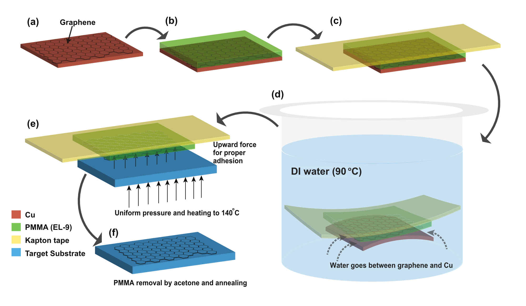
CVD graphene was grown both in continuousLi et al. (2009a) and island growthHan et al. (2012) modes on Cu and Pt substrates (details about the growth provided in Supporting Information section I sup ). The SPeeD transfer process is schematically depicted in Figure 1. After the CVD growth of graphene on Cu foil (Figure 1(a)), we spin-coated the graphene with PMMA ( nm thick resist (Microchem EL ) at a speed of rpm for s) followed by baking for minutes at (Figure 1(b)). To avoid crumpling of the resist after delamination and for easier handling, Kapton tape ( M ) is stuck on the resist and uniform pressure is applied using a teflon roller (Figure 1(c)).
The Cu foil, with the tape attached, is then immersed in a beaker of DI water maintained at for hours (Figure 1(d)). During this period DI water penetrates the graphene-Cu interface. Subsequently, the Kapton tape (to which the PMMA/graphene stack is attached) is slowly peeled away with tweezers leaving behind the Cu foil (see supporting movie S1 which shows the key steps of our SPeeD process sup ).
The target substrate, a nm thick SiO2-coated p-type silicon wafer, was cleaned using oxygen plasma reactive ion etching to ensure better adhesion between graphene and the substrate. The Kapton tape, clamped to a glass slide, and the target substrate are brought into contact and heated for minutes at (Figure 1(e)). After allowing the sample to cool for minutes, the Kapton tape is detached from the glass slide and the stack is put in acetone to remove the EL layer. Subsequently, rapid thermal annealing (RTA) ( for 10 minutes and for 5 minutes in 100 sccm Ar) is done to remove any residual PMMA (Figure 1(f)), thus completing the transfer process.
We used the DI water based SPeeD method to transfer the graphene grown on Pt foils as well. With our technique, this can be easily done without curling of graphene and without using any chemical like NaOH that can lead to unintentional doping of graphene Gao et al. (2012). The only difference from the process for releasing used for graphene on Cu is that a thicker resist layer was used for Pt compared to Cu and the resist was not baked. The remaining procedure for transfer of graphene from Pt is same as that for graphene on Cu.
To benchmark the quality of graphene transferred using our SPeeD based transfer process we transferred two graphene samples, grown on Cu foils from the same batch and in the same graphene growth run, by two different transfer methods. Though the quality of our CVD graphene is not as good as the best reported in the literature Li et al. (2009a, 2011); Reina et al. (2009), the comparison of graphene samples grown in the same run under identical conditions but transferred by different processes should show the influence of the transfer process on the defect level, doping level and quality of graphene. The first sample was transferred onto an SiO2-coated Si substrate using conventional etching of Cu with ammonium persulphate solution (details in Supporting Information section II). The second sample was transferred to an identical substrate using our SPeeD method with DI water without using any etchant. We compare the two samples transferred using Raman spectroscopy measurements Ferrari and Basko (2013) and electrical transport measurements. The results of the comparison are discussed in the following sections.
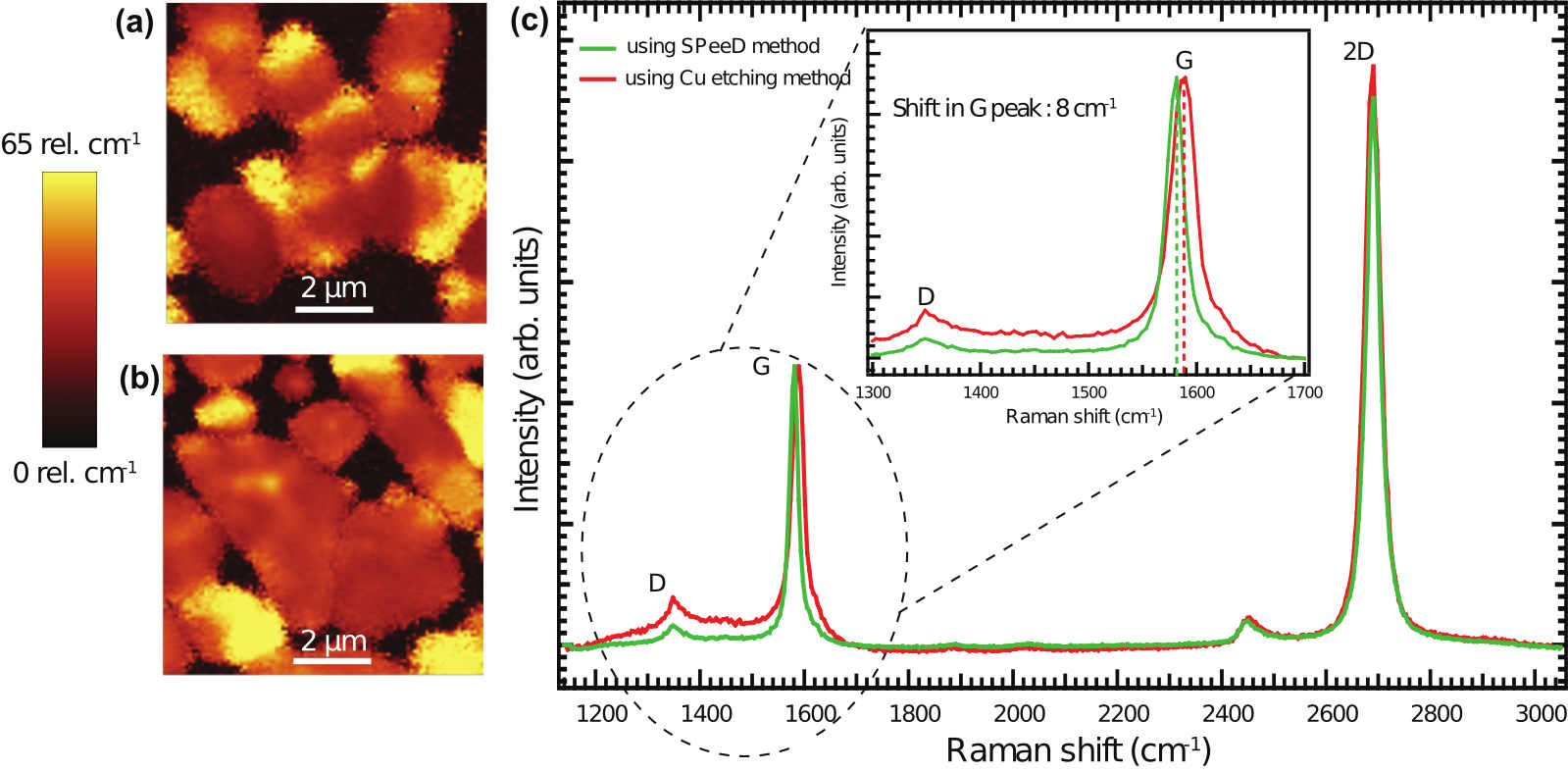
Confocal Raman spectroscopy measurements were performed on both the samples using a WITec Alpha R confocal Raman microscope. Figures 2(a) and (b) compare the Raman maps of the full width at half maximum (FWHM) of the 2D peak for the two graphene samples transferred by the two different methods. The spatially-averaged Raman spectra of graphene over a area for both samples are shown in Figure 2(c). To evaluate shift in peak positions, the spectra are aligned with reference to the Si substrate peak ( cm-1), and to compare relative intensity of the various features, the spectra are intensity normalized to the graphene G peak value. The ratio of the intensity of the 2D peak to G peak in both the samples is comparable and has the value of , which indicates that the graphene is monolayer Ferrari and Basko (2013).
The interesting observation is that the integrated Raman spectrum of the graphene transferred by the SPeeD method has a lower D peak intensity than that of the sample transferred by conventional Cu etching (Figure 2(c)). This suggests that the graphene transferred by the SPeeD process has less defects compared to the one transferred by conventional Cu etching.Ferrari (2007) Further, the inset (Figure 2(c)) shows that the FWHM of the G peak of the graphene transferred by the SPeeD process is narrower than that of the graphene transferred by Cu etching. This points to a lower disorder in the SPeeD transferred sample.Cançado et al. (2011) Additionally, the G peak is blue shifted Das et al. (2008) in the graphene transferred by Cu etching. This indicates that the graphene transferred by Cu etching is p-type doped compared to the other sample Das et al. (2008); Ferrari and Basko (2013). This p-type doping can be attributed to charge impurities present in the Cu etchant or the presence of defects in the graphene. Thus, transferring graphene using our SPeeD method without any use of Cu etchant reduces the probability of graphene getting doped by ionic impurities. Transport measurements on two graphene samples (discussed later) grown using the same recipe but different transfer methods corroborate this observation about reduced doping in the SPeeD transferred samples.
The SPeeD method has been successfully applied to transfer CVD graphene grown on Pt foils as well. Raman measurements on the CVD graphene transferred via the SPeeD method from Pt foils to nm SiO2-coated p-doped Si are shown in Figure 3.
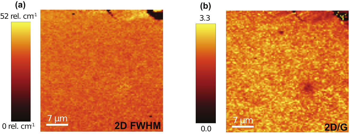
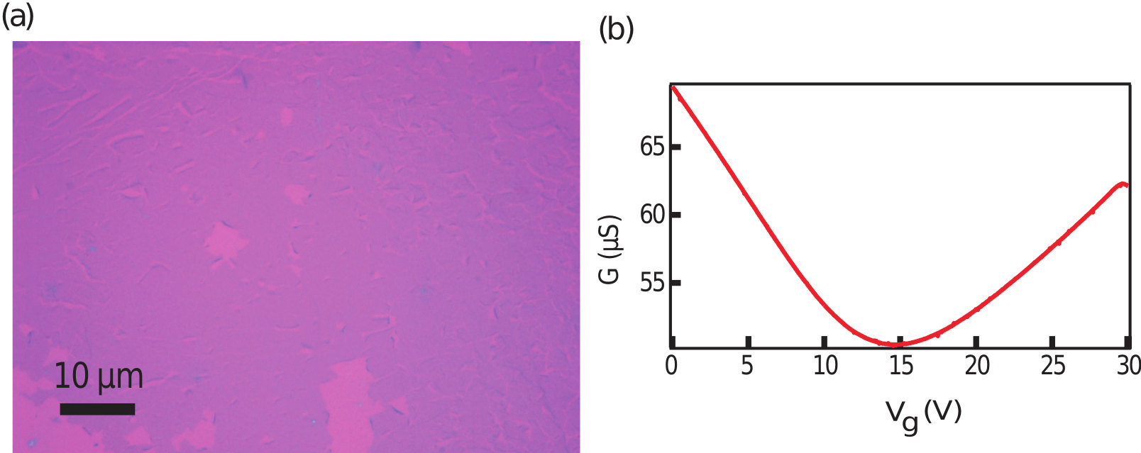
Figure 4(a) shows the optical image of the graphene transferred from Cu substrate by SPeeD method on nm SiO2-coated p-type doped silicon target substrate. Electrical transport measurement data on two graphene samples grown under same conditions, but one transferred via conventional Cu etching and the other via our DI water SPeeD method are shown in Figure 4(b) and (c) respectively.
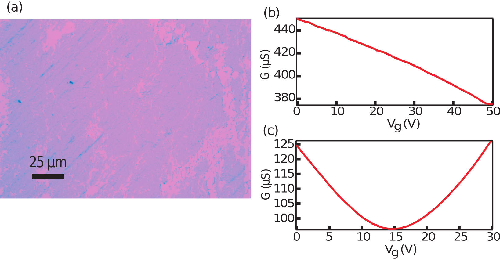
The Dirac point for graphene transferred by Cu etching is shifted in high positive gate voltage region ( V) (Figure 4(b)) indicating that it is highly p-type doped which also agrees well with the Raman measurements. The Dirac point is observable in DI water transferred graphene at V (Figure 4(c)) indicating that the sample is much cleaner in comparison.
An optical image of the graphene transferred from Pt substrate by SPeeD method on nm SiO2-coated p-type doped silicon target substrate is shown in Figure 5(a). The gating curve for the device fabricated using our transfer method shows the presence of the Dirac peak at V (Figure 5(b)) once again showing a relatively clean sample.
In summary, we have successfully demonstrated a novel and simple Soak-and-Peel Delamination method using DI water to transfer CVD-grown graphene from metal substrates like copper and platinum to other substrates of interest. This method does not expose graphene to any harsh chemicals and hence ensures that electrical properties of graphene are not affected. This method is cost effective because no etchant is used and since the metal is not etched it can also be recycled many times reducing large scale production costs. It will also allow the use of single crystals of Cu(111) for improved growth without consuming the copper single crystals. This simple technique demonstrates low cost, clean transfer of graphene and opens doors for its widespread use. The SPeeD process may also provide a generic route to exploit differential hydrophilic/ hydrophobic interactions to delaminate other 2D layered materials from grown substrates.
Acknowledgements.
The work at TIFR was supported by the Government of India.References
- Geim and Novoselov (2007) A. K. Geim and K. S. Novoselov, Nature Materials 6, 183 (2007).
- Castro Neto et al. (2009) A. H. Castro Neto, F. Guinea, N. M. R. Peres, K. S. Novoselov, and A. K. Geim, Reviews of Modern Physics 81, 109 (2009).
- Novoselov et al. (2012) K. S. Novoselov, V. I. Fal’ ko, L. Colombo, P. R. Gellert, M. G. Schwab, and K. Kim, Nature 490, 192 (2012).
- Novoselov et al. (2004) K. S. Novoselov, A. K. Geim, S. V. Morozov, D. Jiang, Y. Zhang, S. V. Dubonos, I. V. Grigorieva, and A. A. Firsov, Science 306, 666 (2004).
- Zhang et al. (2005) Y. Zhang, J. P. Small, W. V. Pontius, and P. Kim, Applied Physics Letters 86, 073104 (2005).
- Stankovich et al. (2007) S. Stankovich, D. A. Dikin, R. D. Piner, K. A. Kohlhaas, A. Kleinhammes, Y. Jia, Y. Wu, S. T. Nguyen, and R. S. Ruoff, Carbon 45, 1558 (2007).
- Hernandez et al. (2008) Y. Hernandez, V. Nicolosi, M. Lotya, F. M. Blighe, Z. Sun, S. De, I. T. McGovern, B. Holland, M. Byrne, Y. K. Gun’Ko, J. J. Boland, P. Niraj, G. Duesberg, S. Krishnamurthy, R. Goodhue, J. Hutchison, V. Scardaci, A. C. Ferrari, and J. N. Coleman, Nature Nanotechnology 3, 563 (2008).
- Berger et al. (2004) C. Berger, Z. Song, T. Li, X. Li, A. Y. Ogbazghi, R. Feng, Z. Dai, A. N. Marchenkov, E. H. Conrad, P. N. First, and W. A. de Heer, The Journal of Physical Chemistry B 108, 19912 (2004).
- Yu et al. (2008) Q. Yu, J. Lian, S. Siriponglert, H. Li, Y. P. Chen, and S.-S. Pei, Applied Physics Letters 93, 113103 (2008).
- Li et al. (2009a) X. Li, W. Cai, J. An, S. Kim, J. Nah, D. Yang, R. Piner, A. Velamakanni, I. Jung, E. Tutuc, S. K. Banerjee, L. Colombo, and R. S. Ruoff, Science 324, 1312 (2009a).
- Sutter, Flege, and Sutter (2008) P. W. Sutter, J.-I. Flege, and E. A. Sutter, Nature Materials 7, 406 (2008).
- Kang et al. (2009) B. J. Kang, J. Hun Mun, C. Y. Hwang, and B. Jin Cho, Journal of Applied Physics 106, 104309 (2009).
- Sutter, Sadowski, and Sutter (2009) P. Sutter, J. T. Sadowski, and E. Sutter, Physical Review B 80, 245411 (2009).
- Wood et al. (2011) J. D. Wood, S. W. Schmucker, A. S. Lyons, E. Pop, and J. W. Lyding, Nano Letters 11, 4547 (2011).
- Geim (2009) A. K. Geim, Science 324, 1530 (2009).
- Reina et al. (2009) A. Reina, X. Jia, J. Ho, D. Nezich, H. Son, V. Bulovic, M. S. Dresselhaus, and J. Kong, Nano Letters 9, 30 (2009).
- Kim et al. (2009) K. S. Kim, Y. Zhao, H. Jang, S. Y. Lee, J. M. Kim, K. S. Kim, J.-H. Ahn, P. Kim, J.-Y. Choi, and B. H. Hong, Nature 457, 706 (2009).
- Bonaccorso et al. (2010) F. Bonaccorso, Z. Sun, T. Hasan, and A. C. Ferrari, Nature Photonics 4, 611 (2010).
- Bae et al. (2010) S. Bae, H. Kim, Y. Lee, X. Xu, J.-S. Park, Y. Zheng, J. Balakrishnan, T. Lei, H. Ri Kim, Y. I. Song, Y.-J. Kim, K. S. Kim, B. Özyilmaz, J.-H. Ahn, B. H. Hong, and S. Iijima, Nature Nanotechnology 5, 574 (2010).
- Gao et al. (2011) M. Gao, Y. Pan, L. Huang, H. Hu, L. Z. Zhang, H. M. Guo, S. X. Du, and H.-J. Gao, Applied Physics Letters 98, 033101 (2011).
- Li et al. (2009b) X. Li, Y. Zhu, W. Cai, M. Borysiak, B. Han, D. Chen, R. D. Piner, L. Colombo, and R. S. Ruoff, Nano Letters 9, 4359 (2009b).
- Wang et al. (2011) Y. Wang, Y. Zheng, X. Xu, E. Dubuisson, Q. Bao, J. Lu, and K. P. Loh, ACS Nano 5, 9927 (2011).
- Gao et al. (2012) L. Gao, W. Ren, H. Xu, L. Jin, Z. Wang, T. Ma, L.-P. Ma, Z. Zhang, Q. Fu, L.-M. Peng, X. Bao, and H.-M. Cheng, Nature Communications 3, 699 (2012).
- Ma et al. (2013) D. Ma, Y. Zhang, M. Liu, Q. Ji, T. Gao, Y. Zhang, and Z. Liu, Nano Research , 1 (2013).
- Schneider et al. (2010) G. F. Schneider, V. E. Calado, H. Zandbergen, L. M. K. Vandersypen, and C. Dekker, Nano Letters 10, 1912 (2010).
- Bonaccorso et al. (2012) F. Bonaccorso, A. Lombardo, T. Hasan, Z. Sun, L. Colombo, and A. C. Ferrari, Materials Today 15, 564 (2012).
- Reina et al. (2008) A. Reina, H. Son, L. Jiao, B. Fan, M. S. Dresselhaus, Z. Liu, and J. Kong, The Journal of Physical Chemistry C 112, 17741 (2008).
- Bianco, Iskrov, and Franzese (2012) V. Bianco, S. Iskrov, and G. Franzese, Journal of Biological Physics 38, 27 (2012).
- Wang et al. (2009) S. Wang, Y. Zhang, N. Abidi, and L. Cabrales, Langmuir 25, 11078 (2009).
- Valette (1982) G. Valette, Journal of Electroanalytical Chemistry and Interfacial Electrochemistry 139, 285 (1982).
- Gardner and Woods (1977) J. Gardner and R. Woods, Journal of Electroanalytical Chemistry and Interfacial Electrochemistry 81, 285 (1977).
- Levendorf et al. (2009) M. P. Levendorf, C. S. Ruiz-Vargas, S. Garg, and J. Park, Nano Letters 9, 4479 (2009).
- Lee et al. (2010) Y. Lee, S. Bae, H. Jang, S. Jang, S.-E. Zhu, S. H. Sim, Y. I. Song, B. H. Hong, and J.-H. Ahn, Nano Letters 10, 490 (2010).
- Regan et al. (2010) W. Regan, N. Alem, B. Alemán, B. Geng, C. Girit, L. Maserati, F. Wang, M. Crommie, and A. Zettl, Applied Physics Letters 96, 113102 (2010).
- Han et al. (2012) Z. Han, A. Kimouche, A. Allain, H. Arjmandi-Tash, A. Reserbat-Plantey, S. Pairis, V. Reita, N. Bendiab, J. Coraux, and V. Bouchiat, arXiv:1205.1337 (2012).
- (36) See supplementary information, high resolution images included in the paper and video for the transfer process at http://www.tifr.res.in/ nano/publications.htm. .
- Li et al. (2011) X. Li, C. W. Magnuson, A. Venugopal, R. M. Tromp, J. B. Hannon, E. M. Vogel, L. Colombo, and R. S. Ruoff, Journal of the American Chemical Society 133, 2816 (2011).
- Ferrari and Basko (2013) A. C. Ferrari and D. M. Basko, Nature Nanotechnology 8, 235 (2013).
- Ferrari (2007) A. C. Ferrari, Solid State Communications 143, 47 (2007).
- Cançado et al. (2011) L. G. Cançado, A. Jorio, E. H. M. Ferreira, F. Stavale, C. A. Achete, R. B. Capaz, M. V. O. Moutinho, A. Lombardo, T. S. Kulmala, and A. C. Ferrari, Nano letters 11, 3190 (2011).
- Das et al. (2008) A. Das, S. Pisana, B. Chakraborty, S. Piscanec, S. K. Saha, U. V. Waghmare, K. S. Novoselov, H. R. Krishnamurthy, A. K. Geim, A. C. Ferrari, and A. K. Sood, Nature Nanotechnology 3, 210 (2008).