For graphene to be utilized in the digital electronics industry the challenge is to create bandgaps of order 1eV as simply as possible. The most successful methods for the creation of gaps in graphene are (a) confining the electrons in nanoribbons, which is technically difficult or (b) placing a potential difference across bilayer graphene, which is limited to gaps of around 300meV for reasonably sized electric fields. Here we propose that electronic band gaps can be created without applying an external electric field, by using the electron-phonon interaction formed when bilayer graphene is sandwiched between highly polarisable ionic materials. We derive and solve self-consistent equations, finding that a large gap can be formed for intermediate electron-phonon coupling. The gap originates from the amplification of an intrinsic Coulomb interaction due to the proximity of carbon atoms in neighbouring planes.
Bias Free Gap Creation in Bilayer Graphene
I Introduction
The experimental discovery of graphene by Novoselov and Geim et al. Discovery has led to a major drive to develop graphene based microelectronics to replace silicon in computing devices. Geim2007 Exceptional electrical, transport and thermodynamic properties make graphene a promising material for this task, although the honeycomb structure naturally leads to a zero-gap semiconductor. The goal is to change the electronic structure to make a useful semiconductor without destroying the properties that make graphene unique. Berger2004
Graphene is both extremely strong and structurally stable, even on very small length scales, due to bonds that connect the carbon atoms together in a hexagonal structure. Therefore, graphene structures have the potential to function on much smaller nanoscales than silicon technology. Ribbons Very large graphene sheets can be manufactured, raising the possibility of creating entire devices from a single graphene sheet.Schwierz2010 Energy loss in such graphene devices would be severely reduced as the number of connections from one material to another inside the devices are minimized, which could lead to smaller and faster chips.Ribbons
There are many proposals for the creation of gaps in monolayer graphene, including the alteration of the structural geometry of the graphene, introduction of impurities (replacing carbon atoms or adding adatoms), creation of graphene quantum dots QuantumDots or by dimensional reduction by making nanoribbons NanoribbonGap . While these methods are very promising in theory, current technology and finite size effects put large scale production outside our reachNilsson2008 , but bilayer graphene may offer a solution. BilayerElectricField ; CoulombBlocade
Bilayer graphene, similar to monolayer, is a zero-gap semiconductor, with valence and conduction bands that meet at the Fermi surface. It is available in two forms with and stacking. Graphene101 If a sufficient electric potential is applied over the two sheets, a gap opens up at the high symmetry and points of the Brillouin zone on the order of the interlayer hopping energy. TheoryGap This effect has been observed experimentally ExperimentGap , where band gaps of -eV are seen, but they require large potential differences to be maintained across the bilayer. Such electronic devices have been predicted to operate with clock speeds in the order of terahertz.TeraHertz Although the bandgaps described above are sufficiently large to make digital transistors, the devices still lack the required properties for large scale production.Schwierz2010
Substrates can also modify the electronic properties of epitaxial graphene Bostwick2007b and contribute to changes in the band structure and resistivity, including electron band gap creation.Zhou2007 ; Enderlein2010 Theoretical works have explored surface reconstructions for graphene on substrates such as SiC Pankratov2010 and possible gap enhancements from interactions between electrons and surface phonons on polarisable substrates. Hague2011
The approach proposed in this paper is different to previous schemes for opening a gap in bilayer graphene since no potential difference across the bilayer is required. While it is often neglected, bilayer graphene has a small inherent difference in electrical potential in the AB stacking configuration; two of the carbon atoms in the unit cell sit directly beneath each other with overlapping electron wavefunctions.Graphene101 We study how this small difference is amplified by an electron-phonon interaction between the bilayer and a sandwich of a highly polarisable sub/super-strate.
This paper is organised as follows. We introduce a model for unbiased bilayer graphene including a Holstein electron-phonon interaction in section II, where we also derive self-consistent equations for the gap. Results showing the evolution of the gap with electron-phonon coupling strength is presented in section III. We summarise the work in section IV, where we also discuss the outlook for observing the gap or its precursor.
II Model and methods
The electron-phonon interaction has been widely studied in condensed matter systems, most notably in theories of superconductivity. Superconductivity There have been several studies of its role in graphene and graphitic structures that are both theoretical Cappelluti2012 ; Stein2013 and experimental Ulstrup2012 ; Fay2011 ; Bruna2010 . This work goes beyond that of previous studies in an attempt to create a usable and tuneable gap in bilayer graphene purely by choosing the materials that surround it.
In this paper, we study the electron-phonon interaction between electrons in the graphene layer and phonons in a surrounding material. To avoid confusion, we point out that the form of electron-phonon interaction between electrons in the graphene layer and phonons that are also in the graphene layer is quite different, and it is expected theoretically that such interactions vanish at the K point, essentially due to the symmetries of the interaction and the phonons (See Refs. Attaccalite2010a, and Park2008a, ). ARPES measurements of graphene on a Cu substrate confirm that as doping decreases, so that the Fermi surface approaches the K point Siegel2012 , the dimensionless effective couping decreases to zero in accordance with the work by Calandra et al. Calandra2007 , indicating that the coupling between graphene and a Cu substrate is very small. On the other hand, the dimensionless electron-phonon coupling can change dramatically on different substrates, and for graphene on SiC, the electron-phonon coupling measured by ARPES Bostwick2007a is essentially independent of the chemical potential as the doping approaches 0.2% per site, with an average value for the dimensionless electron-phonon coupling, , of around , far larger than the predictions of in-plane couplings. Since the in-plane interactions must vanish as doping tends to zero, then any remaining electron-phonon interaction must be a result of interactions with the surrounding material. Calandra et al. Calandra2007 find that the couplings measured by Bostwick et al. cannot be explained by an in-plane electron-phonon coupling. In our opinion, this demonstrates that the substrate is responsible for a completely different form of electron-phonon coupling between electrons in the graphene sheet and phonons within the surrounding material 111We note that it is very difficult to calculate the strength of the electron-phonon coupling ab-initio, which can lead to large differences between theoretical predictions and experimental measurements of Yin2013 . Values of are surprisingly common in condensed matter systems, and have been measured in e.g. Pb and high- superconductors..
We model the electronic structure of bilayer graphene by extending the tight-binding approach that has been highly successful for the study of free-standing graphene.Graphene101 A small energy difference, , is induced by the proximity of stacked sites, plus an additional electron-phonon term representing the effect of introducing coupling with phonons in the substrate and superstrate. The Hamiltonian representing this physics is,
| (1) |
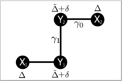
Bilayer graphene has four sites in its unit cell, but symmetry in the lattice shows that there are only two unique sites, that we call X and Y. In eqn. 1, and are operators that creates electrons on sites X and Y respectively, with spin , on layer on the site with lattice vector, (see Fig. 1). The first and second terms represent the contributions of intra-plane and inter-plane hopping to the electron kinetic energy. and are the tight binding parameters for electrons within graphene planes and between graphene sheets respectively.
The electron-phonon interaction is represented by the third term of the Hamiltonian. For interactions between electrons confined to planes, and phonons in surrounding materials, the electron-phonon interaction must have a form where the local electron density couples to displacements of ions in the surrounding material. Here, the standard Holstein approximation is used. determines the magnitude of the interaction between the electron occupation and an ion in the surrounding material displaced by a distance .
The interaction strength, , is directly related to the dimensionless electron-phonon coupling , where is the ion mass and is the phonon frequency. There is no screening between the sub/superstrate and the graphene sheets, which is important for obtaining large electron-phonon coupling strengths. The fourth term in the Hamiltonian describes phonons in the surrounding material as simple harmonic oscillators, where is the phonon number operator.
Strictly, the electron-phonon interaction between the graphene bilayer and the substrate (indeed between any electrons confined to a layer and surrounding ions) would have a Fröhlich form Alexandrov1999 ; Alexandrov2002 ; Steiner2009 , so the results presented here are only expected to be qualitatively similar to the real system. The local Holstein model is a standard approximation to the electron-phonon interaction, chosen here because it significantly simplifies the self-consistent equations, while being in the same general class of interactions Hague2011 . When electron-phonon coupling is moderate, Holstein and Fr¨ohlich interactions lead to qualitatively similar effects on two-dimensional lattices Hague2006 ; Hague2014 .
Finally we add the crucial small energy difference, , between X and Y sites, which originates from the Coulomb repulsion between Y sites on different layers. It is these energy differences that seed the charge density wave state that leads to the band gap.
We compute changes to the effective on-site potentials that occur due to the introduction of the electron-phonon interaction. Perturbation theory was used to obtain self-consistent equations for the change in on-site potentials, a technique that can be highly accurate at low phonon frequency. The order two rotational symmetry means that the simplest solution requires two modified on-site potentials, and . The two functions represent interaction in sites of type X, that only have hopping terms to other atoms in their own layer () and sites of type Y, that interact with the other layer (). The energies involved in the bilayer are summarized in Fig. 1.
We derive self-consistent equations using a general form of the self-energy, which is consistent with the symmetry of the problem:
| (6) |
Here and are the quasi-particle weights, that represent change in the effective mass for the gap functions and respectively. Both and are functions of the fermion Matsubara frequency , where is an integer and is the temperature. Off diagonal terms in the self-energy are zero in the perturbation theory considered here and terms are taken to be momentum independent. This is consistent with a local approximation or dynamical mean-field theory (DMFT).
We construct the full Green’s function of the system using Dyson’s equation, , where the non-interacting Green’s function of the system can be found from :
| (11) |
describes the electron in plane hopping, where we sum over the nearest neighbor vectors, .Graphene101 Self consistent equations for the effective on-site potentials are derived by inverting the Green’s function matrix and then placing it into the 1st order contribution to the self-energy
| (12) |
where the phonon propagator , and is an integer.
We obtain two simultaneous equations from Equation (12) that describe how the effective potential changes with our free parameters; temperature, phonon frequency, on-site potential and electron-phonon coupling constant.
| (13) | |||
| (14) |
is the monolayer density of states (DOS) and . The equations were simplified by the substitution of , , and . ,, and are all taken to be real so each equation is solvable by separation of real and imaginary parts.
III Results
Equations (13) and (14) were solved numerically with a linear approximation to the monolayer DOS, to reduce computation cost. Such an approximation is valid for energies close to the Fermi energy, and differs from the full DOS by less than .
Tight binding parameters of eV, and were used to mimic experimental values.ParameterValues Temperatures of and were explored corresponding to and respectively. Phonon frequencies of meV and meV were also investigated.
 |
 |
 |
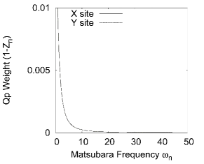 |
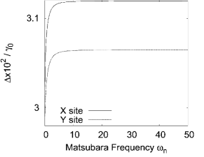
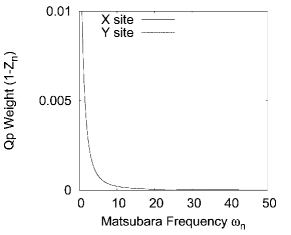
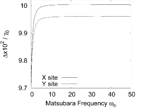
The Matsubara frequency dependance of solutions to Equations (13) and (14) is shown in Figure 2. The electron-phonon coupling strengths used here are indicative of the interactions investigated in this paper: (Top) and (Bottom). In both cases the real part of the self energy for both X and Y sites (which represents the correction to the on-site potential energy), , increases rapidly before levelling off to a constant value by . The associated quasi-particle weight tends to a value of one as the potential function approaches convergence. Sums in the self consistent equations were cut-off at around to ensure numerical convergence over all electron-phonon coupling constants. Both functions are only weakly dependent on the Matsubara frequency, and vary by less than 2% over the range of frequencies. The flat tail at large Matsubara frequency means that the frequency independent parts of the local potentials can be determined for calculation of the real frequency band structure.
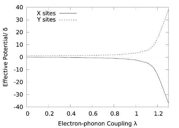
The evolution of the on-site potentials (note that ) with increasing electron-phonon coupling is shown in Fig. 3. It can be seen that the addition of the electron-phonon coupling leads to an increase in the effective for both X and Y sites. This occurs as follows: the small value on the Y sites is amplified by the electron-phonon coupling. An equivalent but opposite effective potential is formed on X sites, which is the same except for the small difference , since charge is conserved during self-consistency. The effective on-site potential has increased to by , and then goes through a rapid increase around with enhancements exceeding . The gap enhancement can be interpreted as an instability to charge density wave order, where electrons are more likely to be found on X sites. The small potential difference between the two sites brings about a variation in the electron density that is amplified by the electron-phonon interaction. Although not fixed in the self-consistency, examination of the figure indicates that the potentials and are related via .
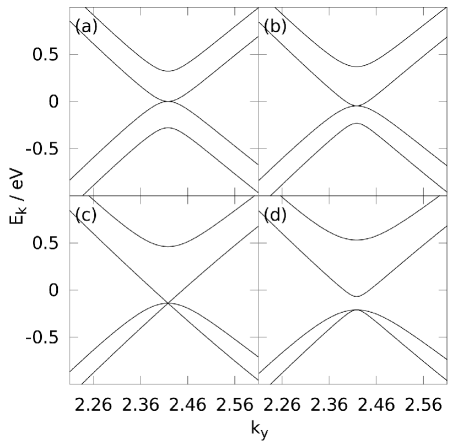
To demonstrate how this leads to band gap creation, Fig. 4 displays the electron band structure close to the K point, for various values of the electron-phonon interaction strength. The bands are calculated along the line (which is also a point at which Dirac cones are observed in monolayer graphene), and is representative of all the high-symmetry points at the Fermi energy. We note that due to symmetry considerations, the effective Hamiltonian for low energy excitations of any system with the bilayer structure will have the same form, even if the origin of the terms in the Hamiltonian are different (for example, the same low energy features due to static Coulomb potentials formed between a graphene monolayer, buffer carbon layer and a SiC substrate can be seen close to the Fermi surface in Ref. Pankratov2010 ) but we show the low energy band structure here to assist the reader to identify the features that may be seen experimentally in the context of specific values of electron-phonon coupling. Figure 4(a) demonstrates the bare bilayer graphene band structure when the electron-phonon coupling is zero and no gap is present, so only is included. Increase in the electron-phonon coupling to (panel b) shifts the lower bands down in energy, but does not lead to qualitative change in the band structure.The lowest energy bands drop slowly with increased until the two bottom bands touch at , and Dirac cones are created. Figure 4(c) is the bilayer graphene band structure when where the system is on the verge of opening a gap, which occurs when the on-site potentials have the value , and dominate the band structure. For the band gap opens up monotonically with increasing . Figure 4(d) shows the gap that has opened when . Strictly, the small Matsubara frequency dependence of and means that the energies in the band structure will be slightly broadened so that the quasi-particles have a finite lifetime, so the band structures shown here are a (close) approximation to the true spectrum of the Green’s functions calculated self-consistently. The lower panel shows the band structure along the high symmetry directions in the Brillouin zone. The main changes to the band structure due to the electron-phonon interaction studied in this paper occur close to the point.
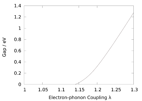
Figure 5 plots the resulting band gap created in the range , as this is where a gap is first formed. Figure 5 shows that the electron-phonon interaction breaks the zero gap semiconductor structure of bilayer graphene. A gap is formed at , that increases rapidly and exceeding that of biased bilayer graphene (which has a plateau when meV) at around . Referring back to the definition of , we note that an increase in or a decrease in would result in an lower electron-phonon gap transition.
The local approximation to the interactions used here is also approximately valid for longer range Fröhlich interactions. Detailed dynamical cluster approximation calculations on monolayers indicate that while enhancement effects are reduced by long range interactions, they are increased by introducing the phonon self-energy (which is not included here to keep the self-consistent equations simple) Hague2014 , such that the overall enhancement predicted here is expected to be broadly accurate. We note that a pure Holstein interaction might be introduced by functionalizing the bilayer with appropriate molecules, since the bonds from the functionalization would act as local oscillators. In such systems, 50% coverage that differentiates between A and B sites could lead to a larger , thus making it easier to open the gap.
IV Summary
In summary, we have investigated the modification of the band structure of unbiased bilayer graphene when electron-phonon coupling is introduced by sandwiching the bilayer graphene with a highly polarizable material. A perturbative analysis was used to calculate the development of a band gap as the electron-phonon coupling constant is varied. We found that with sufficiently large coupling constants, an electron band gap could be created in bilayer graphene without the need for an external potential. There is a large range of band gaps up to eV within the range . These gaps surpass those achievable in biased bilayer systems. It is interesting to note that the addition of a potential difference across the bilayer system breaks the symmetry of the bilayer, and would potentially destroy the gap creating an effective on/off switch in a similar manner to that of a field effect transistor.
Obtaining large values of would be experimentally challenging. It has previously been demonstrated that graphene can be transferred to arbitrary substrates Caldwel2010 so it is possible that a suitable value of could be found optimal choice of the material surrounding the bilayer. In our opinion, this would be achievable since a lot of the experimental effort to date has focused on reducing the interactions with substrates as much as possible to observe the properties of free-standing graphene (such as high mobilities), rather than searching for the highest possible coupling. In spite of this, intermediate electron-phonon coupling strengths between graphene and neighboring materials have been measured for various substrates (including SiC) with electron-phonon coupling that is essentially filling independent at weak dopings of around 0.2%, with an average value of Bostwick2007a ; Gruneis2009 . With a slight increase in doping, experiments indicate that the electron-phonon coupling ranges from 0.2-0.6 and could even be as high as 1 Siegel2012 , so the values required to open a gap are only slightly bigger than the largest that have been experimentally observed (since , a small increase in would suffice). In addition, the value of might be increased by placing the proposed sandwiched sheets under pressure to reduce the distance between graphene and substrate (the pressure would also increase and the other tight binding parameters to varying degrees). Initially, proof-of-concept experiments should focus on the opening of gaps when there is very large coupling to a highly polarizable ionic material surrounding the bilayer, before refining this gap with the use of e.g. spacer layers. Clearly, such systems warrant further study to determine their full potential.
Acknowledgments
We would like to thank Z.Mašín, N.Mason, A.Umerski and J.Fine for useful discussions. JPH would like to acknowledge EPSRC grant No. EP/H015655/1.
References
- [1] K. S. Novoselov, A. K. Geim, S. V. Morozov, D. Jiang, Y. Zhang, S. V. Dubonos, I. V. Crigorieva, and A. A. Firsov. Electric field effect in atomically thin carbon films. Science, 306(5696):666 – 669, 2004.
- [2] A. K. Geim and K. S. Novoselov. Nat. Mater, 6:183, 2007.
- [3] Claire Berger, Zhimin Song, Tianbo Li, Xuebin Li, Asmerom Y. Ogbazghi, Rui Feng, Zhenting Dai, Alexei N. Marchenkov, Edward H. Conrad, Phillip N. First, and Walt A. de Heer. Ultrathin epitaxial graphite: 2d electron gas properties and a route toward graphene-based nanoelectronics. The Journal of Physical Chemistry B, 108(52):19912–19916, 2004.
- [4] Kyoko Nakada, Mitsutaka Fujita, Gene Dresselhaus, and Mildred S. Dresselhaus. Edge state in graphene ribbons: Nanometer size effect and edge shape dependence. Phys. Rev. B, 54:17954–17961, Dec 1996.
- [5] A. Schwierz. Graphene transistors. Nature Nanotechnology, 5:487–496, 2010.
- [6] P. G. Silvestrov and K. B. Efetov. Quantum dots in graphene. Phys. Rev. Lett., 98:016802, Jan 2007.
- [7] Melinda Y. Han, Barbaros Özyilmaz, Yuanbo Zhang, and Philip Kim. Energy band-gap engineering of graphene nanoribbons. Phys. Rev. Lett., 98:206805, May 2007.
- [8] Johan Nilsson, A. H. Castro Neto, F. Guinea, and N. M. R. Peres. Electronic properties of bilayer and multilayer graphene. Phys. Rev. B, 78:045405, Jul 2008.
- [9] Eduardo V. Castro, K. S. Novoselov, S. V. Morozov, N. M. R. Peres, J. M. B. Lopes dos Santos, Johan Nilsson, F. Guinea, A. K. Geim, and A. H. Castro Neto. Biased bilayer graphene: Semiconductor with a gap tunable by the electric field effect. Phys. Rev. Lett., 99:216802, Nov 2007.
- [10] F. Sols, F. Guinea, and A. H. Castro Neto. Coulomb blockade in graphene nanoribbons. Phys. Rev. Lett., 99:166803, Oct 2007.
- [11] A. H. Castro Neto, F. Guinea, N. M. R. Peres, K. S. Novoselov, and A. K. Geim. The electronic properties of graphene. Rev. Mod. Phys., 81:109–162, Jan 2009.
- [12] Hongki Min, Bhagawan Sahu, Sanjay K. Banerjee, and A. H. MacDonald. Ab initio theory of gate induced gaps in graphene bilayers. Phys. Rev. B, 75:155115, Apr 2007.
- [13] Li Yang. First-principles study of the optical absorption spectra of electrically gated bilayer graphene. Phys. Rev. B, 81:155445, Apr 2010.
- [14] Yu-Ming Lin, Keith A. Jenkins, Alberto Valdes-Garcia, Joshua P. Small, Damon B. Farmer, and Phaedon Avouris. Operation of graphene transistors at gigahertz frequencies. Nano Letters, 9(1):422–426, 2009.
- [15] A. Bostwick, T. Ohta, T. Seyller, K. Horn, and E. Rotenberg. Quasiparticle dynamics in graphene. Nature Physics, 3:36–40, 2007.
- [16] S. Y. Zhou, G.H. Gweon, A. V. Fedorov, P. N. First, W. A. de Heer, D.H. Lee, F. Guinea, A. H. Castro Neto, and A. Lanzara. Substrate-induced bandgap opening in epitaxial graphene. Nature Materials, 6:770–775, 2007.
- [17] C Enderlein, Y S Kim, A Bostwick, E Rotenberg, and K Horn. The formation of an energy gap in graphene on ruthenium by controlling the interface. New Journal of Physics, 12(3):033014, 2010.
- [18] O. Pankratov, S. Hensel, and M. Bockstedte. Electron spectrum of epitaxial graphene monolayers. Phys. Rev. B, 82:121416, Sep 2010.
- [19] J. P. Hague. Phys. Rev. B, 84:155438, 2011.
- [20] A.S Alexandrov. Theory of Superconductivity: from weak to strong coupling. Institute of Physics, 2003.
- [21] E. Cappelluti and G. Profeta. Hopping-resolved electron-phonon coupling in bilayer graphene. Phys. Rev. B, 85:205436, May 2012.
- [22] R. Stein, D. Hughes, and Jia-An Yan. Electric-field effects on the optical vibrations in ab-stacked bilayer graphene. Phys. Rev. B, 87:100301, Mar 2013.
- [23] Søren Ulstrup, Marco Bianchi, Richard Hatch, Dandan Guan, Alessandro Baraldi, Dario Alfè, Liv Hornekær, and Philip Hofmann. High-temperature behavior of supported graphene: Electron-phonon coupling and substrate-induced doping. Phys. Rev. B, 86:161402, Oct 2012.
- [24] A. Fay, R. Danneau, J. K. Viljas, F. Wu, M. Y. Tomi, J. Wengler, M. Wiesner, and P. J. Hakonen. Shot noise and conductivity at high bias in bilayer graphene: Signatures of electron-optical phonon coupling. Phys. Rev. B, 84:245427, Dec 2011.
- [25] Matteo Bruna and Stefano Borini. Observation of raman -band splitting in top-doped few-layer graphene. Phys. Rev. B, 81:125421, Mar 2010.
- [26] Claudio Attaccalite, Ludger Wirtz, Michele Lazzeri, Francesco Mauri, and Angel Rubio. Nano Lett., 10:1172–1176, 2010.
- [27] Cheol-Hwan Park, Feliciano Giustino, Marvin L. Cohen, and Steven G. Louie. Nano Lett., 8:4229–4233, 2008.
- [28] David A Siegel, Choongyu Hwang, Alexei V Fedorov, and Alessandra Lanzara. Electron–phonon coupling and intrinsic bandgap in highly-screened graphene. New Journal of Physics, 14(9):095006, 2012.
- [29] M Calandra and F Mauri. Phys. Rev. B, 76:205411, 2007.
- [30] Aaron Bostwick, Taisuke Ohta, Jessica L. McChesney, Thomas Seyller, Karsten Horn, and Eli Rotenberg. Renormalization of graphene bands by many-body interactions. Solid State Communications, 143(1–2):63 – 71, 2007.
- [31] We note that it is very difficult to calculate the strength of the electron-phonon coupling ab-initio, which can lead to large differences between theoretical predictions and experimental measurements of [40]. Values of are surprisingly common in condensed matter systems, and have been measured in e.g. Pb and high- superconductors.
- [32] A. S. Alexandrov and P. E. Kornilovitch. Phys. Rev. Lett., 82:807, 1999.
- [33] A. S. Alexandrov and P. E. Kornilovitch. J. Phys.: Condens. Matter, 14:5337, 2002.
- [34] M. Steiner, M. Freitag, V. Perebeinos, J. C. Tsang, J. P. Small, M. Kinoshita, D. Yuan, J. Liu, and P. Avouris. Nat. Nanotechnol., 4:320, 2009.
- [35] J. P. Hague, P. E. Kornilovitch, A. S. Alexandrov, and J. H. Samson. Effects of lattice geometry and interaction range on polaron dynamics. Phys. Rev. B, 73:054303, Feb 2006.
- [36] J.P. Hague. arXiv:1303.6941.
- [37] L. M. Zhang, Z. Q. Li, D. N. Basov, M. M. Fogler, Z. Hao, and M. C. Martin. Determination of the electronic structure of bilayer graphene from infrared spectroscopy. Phys. Rev. B, 78:235408, Dec 2008.
- [38] Joshua D. Caldwell, Travis J. Anderson, James C. Culbertson, Glenn G. Jernigan, Karl D. Hobart, Fritz J. Kub, Marko J. Tadjer, Joseph L. Tedesco, Jennifer K. Hite, Michael A. Mastro, Rachael L. Myers-Ward, Charles R. Eddy, Paul M. Campbell, and D. Kurt Gaskill. Technique for the dry transfer of epitaxial graphene onto arbitrary substrates. ACS Nano, 4(2):1108–1114, 2010.
- [39] A. Grüneis, C. Attaccalite, A. Rubio, D. V. Vyalikh, S. L. Molodtsov, J. Fink, R. Follath, W. Eberhardt, B. Büchner, and T. Pichler. Electronic structure and electron-phonon coupling of doped graphene layers in . Phys. Rev. B, 79:205106, May 2009.
- [40] Z. P. Yin, A. Kutepov, and G. Kotliar. Phys. Rev. X, 3:021011, 2013.