Intrinsic electron-glass effects in strongly-localized thallium-oxide films
Abstract
Transport measurements made on films of thallium-oxide (n-type semiconductor) are presented and discussed. The focus in this work is on the strongly-localized regime where charge transport is by variable-range-hopping. It is demonstrated that, at liquid-helium temperatures, these films exhibit all the characteristic features of intrinsic electron-glasses. These include a slow (logarithmic in time) conductance-relaxation that may be induced by any of the following protocols: Quench-cooling from high temperatures, sudden change of gate-voltage, exposure to infrared radiation, and stressing the system with a non-Ohmic field. The microstructure of the films are characterized by electron microscopy and their carrier-concentration are measured by Hall effect. Field-effect experiments reveal a memory-dip that has a width compatible with the carrier-concentration of the system as compared with previously studied electron-glasses. It is observed that the common ingredient in all the systems that exhibit electron-glass effects is high carrier-concentration suggesting that their localized sites may be multi-occupied even when deep into the insulating regime. That lightly-doped semiconductors do not show intrinsic electron-glass effects is consistent with this empirical observation. The connection between the memory-dip and the Coulomb-gap is discussed in light of these findings.
pacs:
72.20.Ee 72.20.Ht 72.80.Ng
I Introduction
The interplay between disorder and interactions in Fermi systems has been a challenging field of research and a source of fascination for more than five decades. A prominent representative of this group, the Anderson transition, has been extensively studied both theoretically and experimentally, and at least qualitatively, its equilibrium properties are well understood. On the other hand, the out-of-equilibrium properties of the insulating phase remains ill-understood and controversial. This applies in particular to the ‘electron-glass’ (EG) scenario discussed in several papers 1 ; 2 ; 3 ; 4 ; 5 . The EG phase is expected to arise from the competition between disorder and interactions. It is a generic scenario that applies to all degenerate Fermi systems with localized states interacting via a Coulomb potential. It ought to be observed in any strongly-localized system exhibiting hopping transport. Experimental evidence for glassy effects, however, has been somewhat scarce. Intrinsic EG effects were found in several systems but remarkably none was reported in lightly-doped semiconductors. By ‘intrinsic EG’ we mean that the effects appear systematically for a given substance independently of the way the sample was prepared to achieve the same relevant parameters (resistance at the measuring temperature, dimensionality, and carrier-concentration).
It has been conjectured 6 that the reason for the absence of intrinsic EG effects in lightly-doped semiconductors is their inherently short relaxation-time, which makes it hard to resolve these effects by transport measurements. The short relaxation time of semiconductors was alleged to be due to their low carrier-concentrations n 6 . This has been supported by a recent experiment on phosphorous-doped silicon where ultra-fast relaxation was found 7 . Conductance relaxations that persist for many seconds, and memory effects characteristic of intrinsic electron-glass, seem 6 ; 8 to be peculiar to systems with n510cm.
Intrinsic electron-glass effects were observed in films of crystalline indium-oxide 9 (InO), several versions of amorphous indium-oxide 9 (InO), and, in ultra-thin films of beryllium 10 . In all these materials the carrier-concentration was measured by Hall effect and verified to be in the high-n limit.
In this work we report on the low temperature transport properties of thallium-oxide, which is n-type semiconductor with high carrier-concentration. The microstructure of thallium-oxide films is quite different than those of InO InO, and beryllium. However, strongly-localized films of this material exhibit glassy effects that are essentially identical to those of InO InO, and beryllium. These include logarithmic relaxation of the out-of-equilibrium conductance and a memory-dip (MD) that has all the earmarks of intrinsic electron-glass. The width of the memory-dip exhibited by thallium-oxide is observed to be close to that of the electron-rich version of InO that has similar carrier-concentration. This appears to be in line with a general trend; the MD width of all materials tested so far shows a systematic correlation with carrier-concentration. The possible connection between the memory-dip and the Coulomb-gap, and the origin of similar behavior in granular systems are discussed in light of these findings.
II Experimental
II.1 Sample preparation and characterization
The TlO films used here were e-gun evaporated on room-temperature microscope-slides or, for the field effect measurements, unto the 0.5m SiO layer thermally grown on 100 Si-wafers. The Si wafers were boron-doped (P-type) with bulk resistivity 210-cm deeply into the degenerate regime. They were used in this study as the gate electrode in the field-effect experiments. The substrate was rinsed by ethanol, dried, and was ion-bombarded by O in the vacuum chamber prior to material evaporation. The source material was 99% pure TlO brown powder (American Elements) pressed into the water-cooled copper crucible of the e-gum ficture. Deposition was carried out at (0.5-2)10 Torr oxygen ambience maintained by leaking 99.9% pure O2 through a needle valve into the vacuum chamber (base pressure 10 Torr). Rates of deposition used for the samples reported here were in the range 0.2-4 Å/s monitored in-situ using a quartz thickness-monitor calibrated by a Tolansky interferometer.
The TlO powder temperature during deposition was 60030K, a much lower evaporation temperature than the 1500K used for InO to obtain similar evaporation rates 11 . Another aspect where TlO films differ from InO films is in the way they respond to different post-preparation treatment. In particular, exposing InO to UV radiation breaks oxygen bonds, which upon vacuuming are removed from the sample. This in turn increases the carrier-concentration and decreases the sample resistance 9 . The UV treatment is a reversible process by which a given sample resistance may be changed. It works well in InO films as well as in ZnO crystals 12 where the resistance may be restored by letting oxygen diffuse back into the sample. Films of TlO on the other hand, show no change of resistance when exposed to UV radiation, and are much less susceptible to oxidizing agents than InO. Lacking this flexibility of fine-tuning the disorder, thallium-oxide samples with different resistances have to be made individually. Varying the film thickness in the deposition process was the most effective way to control the sample resistance, and it turned out that small changes around 200Å yielded the range of few k to 100M (at T=4K).
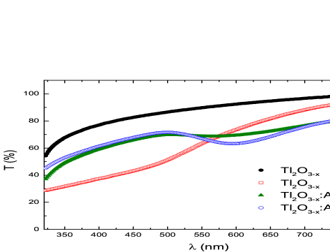
Achieving continuous thin-films of this material is a challenging undertaking. This seems to be a problem that plagues other preparation techniques used to produce thin films of this material 13 . This is the reason for the wide range of rates and oxygen pressure mentioned above that were tested in attempting to find the optimal conditions. Variations in the deposition-rates and partial oxygen pressure had much weaker influence on film structure than the type of substrate used; for nominal thickness in the range 20020 Å the yield of continuous films using (sodium-oxide-rich) microscope-slides was around 80% whereas it was less than 5% (2 in 41 deposition runs) for the SiO layer thermally grown on 100 Si-wafers. Much better yield of physically continuous specimen were obtained on both type of substrates by co-depositing TlO with 6% Au evaporated from a Knudsen source. The gold deposition rate was adjusted independently from that of the TlO. The TlO:Au films turned out to be less sensitive to the type of substrate, and they were also more stable against agglomeration and grain-growth than pure films. Grains as large as 2m could be seen by optical microscopy in TlO samples that were heat-treated at T450K. This agglomeration also affected their optical transmission in the visible as shown in Fig. 1 comparing Au-doped with undoped specimen. Susceptibility to agglomeration and the associated grain-growth is the main impediment in getting electrically continuous thin films of the clean material.
Transmission-electron-microscopy (TEM) was used to characterize the films composition and microstructure (employing the Tecnai F20 G2 equipped with an energy dispersive analyzer). Samples studied by TEM were deposited unto carbon-coated Cu grids under the same conditions as those used for transport measurements. TEM micrographs and electron-diffraction patterns of TlO and TlO:Au films are shown in Fig. 2 and Fig. 3 respectively. The main difference between the two types of the TlO films is the preponderance of smaller and mid-size grains in the TlO:Au films, but both show a rather wide distribution of grain-sizes. This should be compared with the space-filling, mosaic structure of InO films [see e.g., Fig. 1 in 14 ).
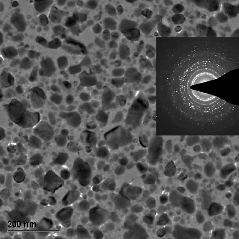
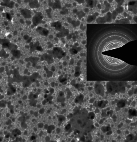
The diffraction patterns of both types of structures are dominated by the larger grains giving spotty rings which mask the presence of an amorphous component in the as-deposited films. The set of rings could be indexed for 8 of the allowed rings according to the bcc bixbyite structure of the compound with lattice spacing a=10.530.02Å (see table 1).
| (hkl) | Observed d (Å) | Calculated d (Å) |
|---|---|---|
| (222) | 3.040.01 | 3.040 |
| (123) | 2.810.01 | 2.814 |
| (400) | 2.640.01 | 2.632 |
| (431) | 2.050.01 | 2.065 |
| (611) | 1.800.01 | 1.806 |
| (622) | 1.590.01 | 1.587 |
| (631) | 1.550.01 | 1.553 |
| (640) | 1.450.01 | 1.460 |
Energy-dispersive x-ray spectroscopy revealed about 1% (atomic ) tungsten as the only contaminant on this level, presumably resulting from spurious deposition off the e-gun filament, as also noticed in InO deposition 11 .
In addition to the rings listed in table 1, TlO:Au films showed a fcc pattern of Au grains suggesting that most of the material segregated out of the TlO matrix. The Au diffraction pattern was used as a guide to calibrate the camera constant. The appearance of free Au particles in the TlO:Au films is another aspect in which this material differs from InO based specimen; in the latter system no sign of free Au is observed in the diffraction patterns for similar levels of gold addition, and there are indications that the gold atoms reside in the oxygen vacancies sites.
Samples used for electrical measurements were deposited through rotatable stainless-steel masks to define their geometry and were typically 1x1mm and 200 Å thick. Prior to sample deposition, gold contacts were evaporated through another set of masks on the same fixture which had alignment pins that positioned the contacts on the sample area.
Room temperature Hall-effect measurements were used to determine the carrier-concentration. This was done with three of the batches prepared for the transport measurements using samples with a Hall-bar configuration (six-probe measured by dc). At room temperatures, these films had sheet-resistances Rof few kmaking them effectively diffusive, and therefore the Hall-effect may be used as a reliable measurement of the material carrier-concentration. Essentially the same result for the carrier-concentration n=(1.90.2)10cm was found for both TlO and TlO:Au films. This value for n is larger by 2-3 than the carrier-concentration found for TlO prepared by electrodeposition 15 and, interestingly, it is almost two orders of magnitude larger than that of InO 11 . No difference in transport properties were found between TlO and TlO:Au films with comparable sheet-resistance R□. It seems that the only role of Au is to curb the tendency of the material to agglomerate.
II.2 Measurement techniques
Conductivity of the samples was measured using a two-terminal ac technique employing a 1211-ITHACO current pre-amplifier and a PAR-124A lock-in amplifier. Most measurements reported below were performed with the samples immersed in liquid helium at T=4.1K maintained by a 100 liters storage-dewar, which allowed long term measurements of samples as well as a convenient way to maintain a stable temperature bath. Unless otherwise indicated, the ac voltage bias was small enough to ensure linear response conditions (judged by Ohm’s law being obeyed within the experimental error).
The microwaves experiments employed high-power synthesizer (HP8360B) using power up to 25 dBm (316 mW) at the frequency range of 2-6 GHz. Optical excitation was accomplished by exposing the sample to AlGaAs diode (operating at 0.880.05m), placed 15mm from the sample. The diode was energized by a computer-controlled Keithley 220 current-source. The samples were attached to a probe equipped with calibrated Ge and Pt thermometers and were wired by triply-shielded cables to BNC connectors at room temperatures. The effective capacitance of the wires was typically 10nF allowing the use of 70-75Hz ac technique in most cases.
Fuller details of measurements techniques are given elsewhere 9 .
III Results and discussion
III.1 Hopping conductivity and current-voltage characteristics
We start this section by examining the near-equilibrium (conductance) and steady-state (current-voltage characteristics) properties of the thallium-oxide films with R□h/e (at liquid helium temperature). The only goal in this section is to demonstrate that the TlOsamples are in the strongly-localized regime, and that their near-equilibrium transport properties cannot be distinguished from those of other hopping systems (including systems that do not exhibit intrinsic electron-glass effects, e.g., lightly-doped semiconductors).
The strongly-localized nature of these films was verified by measuring their conductance versus temperature dependence G(T) at the temperature range 4-45K. Figure 4 illustrates this behavior for two of the samples that were used in this study. Below10K, this dependence can be described reasonably well by G(T)[-(T/T)] with x either 3 or 4. The limited range of temperature and resistance does not allow distinguishing between these. However, this range is wide enough to rule out G(T)[-(T/T)] at least for the sample with the larger resistance in Fig. 4. The form of variable-range-hopping (VRH) shown in Fig. 4 is often observed in strongly-localized InO samples 16 . By comparison, over a similar range of temperatures the hopping law G(T)[-(T/T)] is obeyed by thin films of beryllium 10 , and by the high-carrier concentration version of InO (with n10cm) 17 .
One should not take these mathematical fits too seriously. It is actually unclear why these systems should exhibit any specific exponent of VRH; Both, the ln(G)T and ln(G)T VRH forms are results of models that assume, among other things, single occupation of localized sites. As remarked elsewhere 16 , this assumption may not justified in systems with carrier-concentration as high as that of InO(let alone in systems with higher n such as Be and InO). In these systems there are many charge-carriers within a localization volume and interactions may modify overlapping electronic states.
There are apparently other factors in hopping conductivity that are not accounted for by existing theories. A pertinent comment on the uncertainty of the hopping exponent in realistic systems was made by Brodsky and Gambino on the basis of their experiments in amorphous Si 18 (where multi-occupation of localized states is not a concern). Rather, it was the behavior of the pre-exponential factor that led these authors to remark that not much weight should be given even to the value of the exponent when fitting G(T) data. The point is that in reality disordered systems are more complicated than assumed by current theories for hopping conductivity. It is hardly surprising that important deviations from the predictions of hopping models are observed in experiments on real samples. Nonetheless, the exponential temperature dependence of G is a clear indication of the strongly-localized nature of the used films and that is all we need for the main conclusions in this paper.

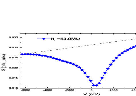
A characteristic attribute of hopping systems, which further illustrates the inadequacy of current VRH models, is their non-Ohmic behavior, which is often observable at lower fields F than anticipated. The common expectation is that Ohmic behavior persists up to fields of order kT/eL where e is the electron charge and L is the percolation radius 19 . However, typical values for L determined from the crossover to non-Ohmic behavior often leads to values of L that are much larger than this length scale 20 ; 21 ; 22 . The same phenomenon is observed in all our TlO and TlO:Au samples. Figure 5 shows the dependence of the conductance on the applied voltage for a typical TlO:Au sample.
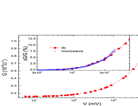
The inset to Fig. 5 is a zoom-in on the low voltage part of the main G(V) curve taken by a low-frequency ac technique. It is hard to assign a precise value for the voltage above which Ohmic behavior is no longer obeyed in the G(V) curve as the deviation is gradual. A fair estimate based on the data shown in the inset to Fig. 5 would be V30mV where the deviation from Ohmic behavior is well above the experimental error. Using LbkT/eV (b is the sample length) gives L 10m, which is much larger than any reasonable estimate for the percolation radius. This problem seems to be the rule in VRH conductivity; similarly large values for L were found by Rosenbaum et al 20 in doped-Si, and Grannan et al 22 found in Ge samples doped by nuclear transmutation.The possibility that these discrepancies arise from the present of long-rnage potential fluctuations was discussed in 20 , and experimntal evidence for their presence was found in strongly insulating InO and InO films 23 .
Finally, the change of the conductance due to application of a microwave field is compared in Fig. 5 (inset) with the G(V) data taken at a low frequency. In the latter case G is still measured at low frequency but as function of the amplitude of a microwave field capacitively coupled to the sample 24 . This microwave enhanced conductivity is another way to modify the hopping conductance and it is essentially a non-Ohmic effect generic to VRH systems. This was shown to exist in several systems including in the lightly-doped GaAs 24 . It was also pointed out that existing models for non-ohmicity in the VRH regime fail to give a satisfactory fit to the experimental G(V) in these systems 24 .
To sum up this part we conclude that thallium-oxide samples with R□h/e (at T4K) exhibit VRH behavior that is similar to other strongly-localized systems including some lightly-doped semiconductors. Their out-of-equilibrium transport features described next, identify them as intrinsic electron-glasses with extended relaxation times as might be expected from their high carrier-concentration on the basis of previous empirical findings. These, as will be discussed below, cannot be accounted for by VRH models that assume single occupation of localized sites.
III.2 Out of equilibrium transport properties
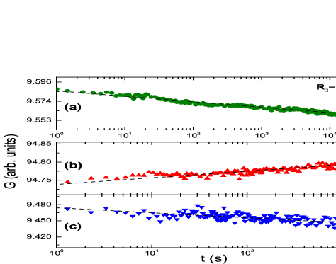
The first set of experiments, shown in Fig. 6, describes the basic relaxation of the excess conductance following quench-cooling the sample from high temperatures to liquid helium ambience (Fig. 6a). Fig. 6b&c show the results of applying the stress-excitation protocol 25 on the same sample after it was allowed to equilibrate at T=4.1K for 28 hours. The stress protocol involves subjecting the sample to a large ‘source’-‘drain’ field, driving the sample into the non-Ohmic regime, which creates excess phonons and takes the system out of equilibrium. This can be observed during the stress as a slow increase of the conductance (Fig. 6b), and when Ohmic conditions are restored a logarithmic decay of the excess conductance is observed (Fig. 6c).
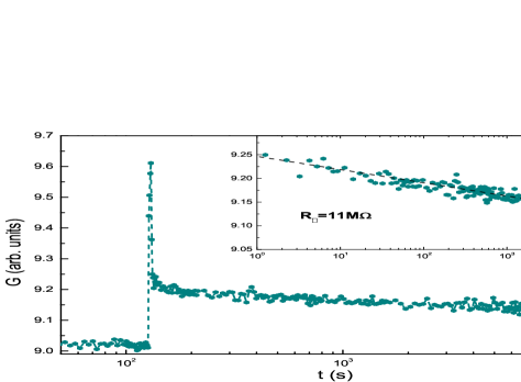
Another effective way to drive the system far from the equilibrium and observe the ensuing relaxation is by optical excitation. A typical result using this protocol is illustrated in Fig. 7 for a TlO film.
Common to the protocols used in Figs. 6 and 7 is that they can be performed on films deposited on any insulating substrate and do not necessitate a gate.
This makes it easier to measure the conductance of a high resistance sample. A nearby metallic gate, a must for the field effect experiments, introduces a parallel capacitance in the measurement circuit and limits the frequency used in the ac technique. Also, comparing the results with TlO samples configured with a gate helps to verify that the glassy effects are not due to artifacts associated with trapped charge or other defects in the insulating layer that separates the sample from the gate (this appears to be a problem in some semiconductors). However, as was emphasized elsewhere 6 , the prime signature for an intrinsic electron-glass is a memory-dip which can only be tested via the field-effect technique. A major effort was therefore dedicated to produce gated structure for field effect experiments. Five TlO:Au films with sheet resistances R□ between 800k to 30M configured with a gate for field-effect experiments. The MD for the highest R□ film tested in a MOSFET configuration is shown in Fig. 8.
As in other electron-glasses, the width of the MD turns out to be independent of R□ over the range studied 9 . Note that is comparable to that of the electron-rich version of InO that has a similar value of carrier-concentration n as our TlO:Au films, as can be seen in Fig. 9a. The significance of this observation will be discussed later.
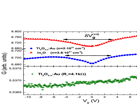
The presence of a memory-dip in the G(V) scans is only observable at T=4K for samples with R200k. Figure 9b shows, on the same gate-voltage scale, the field effect taken with another FET-like structure on a TlO:Au film with a lower disorder. This sample had R□h/e and, at this temperature is in the diffusive regime which, as might be expected, shows no sign of a MD. Rather, the G(V) curve in Fig. 9b exhibits only the thermodynamic field-effect as a slightly concave G(V) curve presumably reflecting the energy dependence of the density of states . The curvature of this curve is typical to a disorder-modified at the tail of the conduction band (note that the Fermi energy associated with n10cm is near the bottom of the band). The G/V0 is consistent with the material being n-type degenerate semiconductor 15 .
The thermodynamic contribution to the field-effect is observable whether the system is glassy or not. For samples in the glassy regime it appears as an anti-symmetric component in G/V. Another way to see the relative contributions of the non-equilibrium and thermodynamic components is in the temporal response of the conductance to a one-step change in V. An example of such a protocol is illustrated in Fig. 10. This is another method of driving the system out of equilibrium and observe the ensuing relaxation.
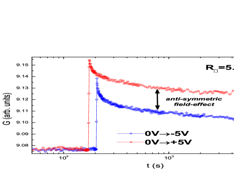
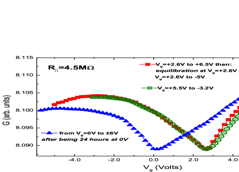
There are two fundamental properties that the memory-dip exhibits. First, its position on the gate-voltage scale, that in the above plots is centered at V=0, depends on the gate-voltage at which the system was allowed to equilibrate. Secondly, it has a characteristic shape that does not depend on whether it was recorded by starting the sweep away from the equilibrium V towards either polarity or by sweeping V through the equilibrium point. These two features, previously studied in the InO and InO samples 9 , are illustrated in Fig. 11. The figure shows a set of recorded events where initially the sample was cooled and equilibrated while holding the gate-voltage at V=+2.6V. After equilibration, the two different sweep protocols were taken to show that the MD is now centered at +2.6V, and that the shape of the MD is essentially the same for both protocols. Then, V was moved to V=0V and it was held there for 24 hours. Subsequent scans of V now reveal the MD centered at the new equilibration position while the old MD has almost vanished (leaving a small bulge at the right-wing of the ‘new’ MD).
The non-equilibrium transport features described above are remarkably similar to those reported in other intrinsic electron-glasses in all aspects and, in particular, in the phenomenology associated with the MD. To see how the width of the MD fits the dependence on carrier-concentration we give in Fig. 12 the width of other non-granular electron-glasses measured to date. In the figure is given in energy units calculated from the experimentally measured width V (see e.g., Fig. 9a) by: . Here C is the sample-to-gate capacitance (per unit area), () the material DOS at the Fermi energy, e is the electron-charge, and is the screening-length. () and were estimated from the material carrier-concentration n using free-electron formulae. The values of obtained in this way are shown in figure 12 as a function of the inter-carrier distance rn. The carrier-concentration n is based on Hall effect measurement performed for each sample included in the figure. The single data point for InO is actually the averaged value for 24 measured samples. Similarly, the data for beryllium is the average of 9 samples 10 , the data for InO:Au is based on 5 samples, and the data for TlO:Au is based on the 5 samples of the present study. Amorphous indium-oxide, InO, is the only EG material studied to date where a study of samples over a wide range of n has been achievable. However, all the other systems follow the same systematic dependence on n as the InO samples.
It is noteworthy that every granular metal that has been tested show electron-glass effects that are quite similar to those of the Anderson insulators in Fig. 12. The studied granular materials include granular-Pb 26 , granular-Al 27 , and discontinuous films of Au 28 , Ni and Ag 29 . In the hopping regime, all these systems exhibit a memory-dip with values that are at the high end of the group depicted in Fig. 12. These are not shown in the figure because their carrier-concentration was not measured. Nonetheless, it is plausible that n in such systems is on the high side, which lends further support to the correlation between carrier-concentration and .
In an earlier work where (n) was studied (Fig. 4 in 8 ), the possible connection between the MD and the Coulomb-gap was considered. Some of the reservations raised in 8 with this line of interpretation were later relaxed 6 . The correlation between that by now has been fortified by adding more samples and three more Anderson insulators, is suggestive of a generic mechanism. This lead us to re-examine the connection between the Coulomb-gap and the memory-dip.
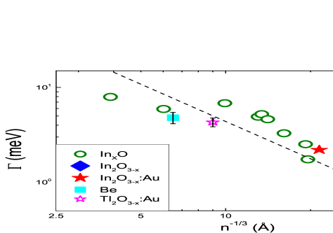
The Coulomb gap (CG), first discussed by Pollak 30 and Srinivasan 31 is a consequence of the loss of screening in the disordered medium, which makes the interaction long-ranged. Efros and Shklovskii has shown how this leads to a soft gap in the single-particle DOS of the system. There are two features of the CG that are reminiscent of the memory-dip main characteristics. First, the CG is a depression in the single particle density of states N() with its minimum pinned to the Fermi energy . This would be a natural explanation for the observation that the MD is centered at the gate-voltage at which the system equilibrated as well as for the two-dip-experiment (Fig. 11 above, 8 ; 9 and references therein). Secondly, the correlation between the MD width and carrier-concentration (Fig. 7) is also in accord with the CG scenario; it is expected that the energy scale due to interactions will be larger in systems with higher carrier-concentration.
The possible relevance of the Coulomb-gap to the non-equilibrium features observed in the intrinsic electron-glasses was considered by Clare Yu 32 ; 33 and by Lebanon and Müller 34 ; 35 . Yu has adopted the Efros-Shklovskii approach according to which the Coulomb-gap determines the system conductance. This allowed her to reproduce the evolution with time of the MD following a quench from high temperatures. Lebanon and Müller, based on similar ideas, developed a model that accounts for many of the observed electron-glass features. In particular, they gave a plausible interpretation to the temperature dependence of the MD shape 34 . This is one of the features that distinguishes the MD of the electron-glass from the cusp that appears in the structural two-level-system 36 ; 37 ; the shape of the cusp in the structural two-level system does not change with temperature whereas the MD shape is very sensitive to temperature 6 ; 9 .
The consistency of the theoretical approaches 32 ; 33 ; 34 ; 35 with the main features of the experiments is encouraging. It does look as a step in the right direction. At the same time, there are questions of fundamental nature that should be addressed. The first question is the subtle issue of the connection between a single-particle DOS and any equilibrium (or near equilibrium) quantity like conductivity. Patrick Lee has commented on this issue with regard to the Thomas-Fermi screening length and the use of the Einstein relation 38 . He pointed out that in both cases it is the thermodynamic DOS that is the relevant quantity.
The single-particle DOS is relevant for processes associated with insertion (removal) of a particle into (from) the system while no relaxation of other particles takes place, which would be the case in tunneling or photoemission events. By contrast, the field effect is usually conceived in the same category as conductance in this respect.
In the current situation we are in an uncharted territory; the process of sweeping the gate voltage involves inserting (removing) particles while ”some fast things have happened but some slow things have not”, which means: things are changing even as we sweep. Under these nonequilibrium conditions it is not clear whether the use of the Einstein relation is justified. One may argue that if the sweep duration is short relative to the relaxation time (yet keeping Vg/t small enough to minimize the risk of structural changes that may be caused by the sweep), the situation is no different than the near-equilibrium conditions encountered in real-life situations. There are no indication from our non-equilibrium field-effect experiments to contradict this point of view. In fact, the dependence of the MD magnitude on the gate-voltage scan-rate seems to be consistent with it; it is found (Fig. 4 in 6 ) that the MD magnitude increases with the scan-rate with the same logarithmic law that controls the time-relaxation of the excess conductance. It may be said that G(V) is a snap-shot of a DOS made observable by a scan that occurred while some particles in the system are effectively frozen. Whether these crude ideas are justified or not must await a proper theory for field-effect experiments in out-of-equilibrium situations.
Even if it is the single-particle DOS that modulates G(Vg), it is not clear what functional form should be taken for it. The problem is not only the multitude of forms derived for the Coulomb gap by different authors 39 ; 40 ; 41 ; 42 ; 43 ; 44 ; 35 , it is rather the basic model used; essentially all Coulomb-gap models assume single-occupation of sites while the one features common to all systems that exhibit MD is that their localized states contain many particles even for strong disorder. There were several attempts to include quantum effects to assess their modifications to the Coulomb gap 40 ; 41 ; 45 ; 46 ; 47 ; 48 ; 49 ; 50 . There were also some attempts to consider double-occupation of the localized states that already introduced new effects that are manifested in magneto-conductance measurements 51 . However, to our knowledge, no treatment of the Coulomb gap for the multi-occupation scenario has been attempted.
The observation that a memory-dip is seen only in electronic systems containing many particles in a localization volume even when strongly localized 52 may be an important clue to the dynamics of the electron-glass. Multiply-populated localized-sites are essentially small (disordered) metals. Tunneling transitions between these mesoscopic elements would induce a many-body shake-up process which may reduce transition probabilities due to the Anderson orthogonality-catastrophe (AOC) 53 . While this is probably a small effect for transport, it may be significant factor in determining the relaxation rate. The space-energy charge organization, building up the Coulomb-gap from the out of equilibrium random distribution, involves many more sites than those participating in the transport. Moreover, many-sites simultaneous transitions are required to approach the lowest energy configuration, while transport is essentially a single-particle process. The necessity of many-particle transitions for achieving the ground state was realized by Baranovski et al in computer simulations 54 .
In sum, we presented data on the structure and transport properties of thallium-oxide films. In the Anderson insulating regime these films exhibit hopping conductivity and current-voltage characteristics that are commonly found in other insulating systems at low temperatures. Their non-equilibrium transport features are in line with those previously reported in other electron-glasses. In particular, they exhibit a memory-dip that is characterized by an energy width that fits the empirical relation relating the width to the carrier-concentration of the material. This feature makes it a challenge to account for the memory-dip by a mechanism that links the glassy effects with 1/f noise 55 .
A common feature shared by all the systems that exhibit intrinsic electron-glass behavior is high carrier-concentration. This presumably is what distinguishes them from the lightly-doped semiconductors. Near the transition to the diffusive regime (or when the dielectric constant of the medium is very large), the electron-electron interaction will be much smaller than the disorder and therefore the element of frustration, crucial for glassy behavior, may not be fulfilled. Both strong disorder and comparably strong interactions are presumably needed for the glassy phase.
Empirically, Anderson insulators with higher carrier-concentration tend to exhibit long relaxation times. Granular metals present a special case of strongly-localized systems with high carrier-concentration and it is remarkable that they systematically exhibit MD and long relaxation times. Note that the other feature they share with the systems in Fig. 12 is many electrons per ‘localization volume’. The empirical evidence in favor of the conjecture that multi-occupation is the reason for the long relaxation times is compelling enough to warrant a serious theoretical effort to explore the possibility that many-body effects are involved.
To further test the empirical connection between carrier concentration and relaxation time, it is desirable to include more materials in the experimental study. Both low and high carrier-concentration should be tested. On the theoretical side, there is the challenge of dealing with the consequences to hopping transport due to multi-occupation of electronic states, and the connection between the single-particle DOS and conductivity in non-equilibrium situations.
Acknowledgement 1
I am indebted to Dr. Tsirlina for drawing my attention to the special qualities of thallium-oxide and for sharing her experience in sample preparation. This research has been supported by a grant administered by the Israel Academy for Sciences and Humanities.
References
- (1) M. Grünewald, B. Pohlman, L. Schweitzer, and D. Würtz, J. Phys. C, 15, L1153 (1982).
- (2) M. Pollak and M. Ortuño, Sol. Energy Mater., 8, 81 (1982).
- (3) M. Pollak, Phil. Mag. B 50, 265 (1984).
- (4) J. H. Davies, P. A. Lee, and T. M. Rice, Phys. Rev. Lett., 49, 758 (1982); ibid, Phys. Rev. B 29, 4260 (1984).
- (5) Ariel Amir, Yuval Oreg, and Yoseph Imry, Phys. Rev. B 77, 165207 (2008); ibid. Annu. Rev. Condens Matter Phys. 2, 235 (2011). The mean field approach in these papers has been recently elucidated by E. Bardalen, J. Bergli, and Y. M. Galperin, Phys. Rev. B 85, 155206 (2012). For a recent review see: M. Pollak, M. Ortuño and A. Frydman, The Electron Glass, Cambridge University Press, 2013.
- (6) Z. Ovadyahu, Phys. Rev. B 78, 195120 (2008).
- (7) V. K. Thorsmølle, and N.P. Armitage, Phys. Rev. Lett. 105, 086601 (2010).
- (8) A. Vaknin, Z. Ovadyahu, and M. Pollak, Phys. Rev. Lett., 81, 669 (1998).
- (9) A. Vaknin, Z. Ovadyahu, and M. Pollak, Phys. Rev. Lett., 84, 3402 (2000).
- (10) Z. Ovadyahu, X. M. Xiong, and P. W. Adams, Phys. Rev. B 82, 195404 (2010).
- (11) Z. Ovadyahu, B. Ovryn and H.W. Kraner, J. Elect. Chem. Soc. 130, 917 (1983).
- (12) O. Cohen, Z. Ovadyahu, and M. Rokni, Phys. Rev. Lett., 69, 3555 (1992); O. Cohen and Z. Ovadyahu, Phys. Rev. B 50, 10442 (1994).
- (13) A. D. Berry, R. T. Holm, R. L. Mowery, N. H. Turner, and M. Fatemi, Chem. Mater., 77, 3 (1991).
- (14) Z. Ovadyahu, J. Phys. C: Solid State Phys., 19, 5187 (1986).
- (15) Robert A. Van Leeuwen, Chen-Jen Hung, Daniel R. Kammler, and Jay A. Switzer, J. Phys. Chem., 99, 15247 (1995).
- (16) A. Vaknin, A. Frydman, Z. Ovadyahu, and M. Pollak, Phys. Rev. B 54, 13604 (1996).
- (17) Entin-Wohlman and Z. Ovadyahu, Phys. Rev. Lett., 56, 643 (1986).
- (18) M. H. Brodsky and R. J. Gambino, Journal of Non-Crystalline Solids, 8-10, 739 (1972).
- (19) B. I. Shklovskii, Fiz. Tekh. Poluprovodn. 6, 2335 (1972) [Sov.Phys. Semicond. 6, 1964 (1973)].
- (20) T. F. Rosenbaum, K. Andres, and G. A. Thomas, Solid State Commun., 35, 663 (1980).
- (21) Ning Wang, F. C. Wellstood, B. Sadoulet, E. E. Haller, and J. Beeman, Phys. Rev. B 41, 3761 (1990).
- (22) S. M. Grannan , A. E. Lang, E. E. Haller, and J .W. Beeman, Phys. Rev. B 45 4516 (1992 ).
- (23) D. Kowal and Z. Ovadyhau, Physica C, 468, 322 (2008).
- (24) Z. Ovadyahu, Phys. Rev. B 84, 165209 (2011); ibid, Phys. Rev. Lett., 102, 206601 (2009). These papers also demonstrate that, at least near the onset for non-Ohmicity, the non-linearity is not due to heating.
- (25) V. Orlyanchik and Z. Ovadyahu, Phys. Rev. Lett., 92 (2004) 066801.
- (26) G. Martinez-Arizala, D. E. Grupp, C. Christiansen, A. Mack, N. Markovic, Y. Seguchi, and A. M. Goldman, Phys. Rev. Lett., 78, 1130 (1997). G. Martinez-Arizala, C. Christiansen, D. E. Grupp, N. Markovic, A. Mack, and A. M. Goldman, Phys. Rev. B 57, R670 (1998).
- (27) T. Grenet, Eur. Phys. J, 32, 275 (2003); T. Grenet, J. Delahaye, M. Sabra, and F. Gay, Eur. Phys. J. B 56, 183 (2007); Delahaye, T. Grenet and F. Gay, Eur. Phys. J. B 65, 5 (2008).
- (28) C. J. Adkins, J. D. Benjamin, J. M. D. Thomas, J. W. Gardner, and A. J. McGeown, J. Phys. C: Solid State Phys. 17, 4633 (1984).
- (29) Tal Havdala, Ariel Eisenbach and Aviad Frydman, EPL, 98, 67006 (2012).
- (30) M. Pollak, Discuss. Faraday Soc. 50, 13 (1970).
- (31) G. Srinivasan, Phys. Rev. B 4, 2581 (1971).
- (32) C. C. Yu, Phys. Rev. Lett., 82, 4074 (1999).
- (33) C. C. Yu Phil. Mag. B, 81, 1209 (2000).
- (34) Eran Lebanon, and Markus Mueller, Phys. Rev. B 72, 174202 (2005).
- (35) M. Müller and E. Lebanon, J. Phys. IV France, 131, 167 (2005).
- (36) Douglas Natelson, Danna Rosenberg, and D. D. Osheroff, Phys. Rev. Lett. 80, 4689 (1998).
- (37) S. Ludwig, P. Nalbach, D. Rosenberg, and D. Osheroff, Phys. Rev. Lett. 90, 105501(2003).
- (38) P. A. Lee, Phys. Rev. B 26, 5882 (1982). See also the pertinent discussion on screening in: M. Lee, J. G. Massey, V. L. Nguyen, B. I. Shklovskii, Phys. Rev. B 60, 1582 (1999).
- (39) A. L. Efros, Phys. Rev. Lett. 68, 22081 (1992).
- (40) A. Möbius, M. Richter, and B. Drittler, Phys. Rev. B 45, 11568 (1992).
- (41) E. Cuevasa and M. Ortuño, Phil. Mag. B, 65, 681 (2005).
- (42) Torsten Wapplerr, Thomas Vojta, and Michael Schreiber, Phys. Rev. B 55, 6272 (1997).
- (43) Thomas Vojta and Michael Schreiber, Phys. Rev. B 49, 7861 (1994).
- (44) Martin Goethe and Matteo Palassini, Phys. Rev. Lett. 103, 045702 (2009).
- (45) Brigitte Surer, Helmut G. Katzgraber, Gergely T. Zimanyi, Brandon A. Allgood, and Gianni Blatter, Phys. Rev. Lett. 102, 067205 (2009).
- (46) G. Vignale, Y. Shinozuka, and W. Hanke, Phys. Rev. B 34, 3003 (1986).
- (47) G. Vignale, Phys. Rev. B 36, 8192 (1987).
- (48) Q. Li and P. Phillips, Phys. Rev. B 48, 15035 (1993).
- (49) T. Vojta and M. Schreiber, Philos. Mag. B 81, 1117 (2001).
- (50) M. Pino, A. M. Somoza, and M. Ortuño, Phys. Rev. B 86, 094202 (2012).
- (51) A. Kurobe and H. Kamimura, J. Phys. Soc. Japan, 51, 1904 (1982). See reference 16 for experimental studies of these effects on several systems.
- (52) Near the transition to the diffusive regime (or when the dielectric constant of the medium is very large), the electron-electron interaction will be much smaller than the disorder and therefore the element of frustration, crucial for glassy behavior, may not be fulfilled.
- (53) Z. Ovadyahu, Phys. Rev. Lett., 99, 226603 (2007).
- (54) S. D. Baranovski, A. L. Efros, B. L. Gelmont, and B. I. Shklovskii, J. Phys. C: Solid State Phys., 12, 1023 (1979).
- (55) See for example: V. I. Kozub, Y. M. Galperin, V. Vinokur, and A. L. Burin, Phys. Rev. B 78, 132201 (2008) and references therein. Some qualitative features of the memory-dip were accounted for by this model.