Evidence for topological band inversion of the phase change material Ge2Sb2Te5
Abstract
We present an angle-resolved photoemission study of a ternary phase change material, namely Ge2Sb2Te5, epitaxially grown on Si(111) in the metastable cubic phase. The observed upper bulk valence band shows a minimum at being 0.3 eV below the Fermi level and a circular Fermi contour around with a dispersing diameter of Å-1. This is in agreement with density functional theory calculations of the Petrov stacking sequence in the cubic phase which exhibits a topological surface state. The topologically trivial cubic KH stacking shows a valence band maximum at in line with all previous calculations of the hexagonal stable phase exhibiting the valence band maximum at for a trivial topological invariant and away from for non-trivial . Scanning tunneling spectroscopy exhibits a band gap of 0.4 eV around .
pacs:
71.20.Nr,73.20.AtI Introduction
Following the proposalVolkov and Pankratov (1985); Fu et al. (2007) and discoveryKönig et al. (2007); Hsieh et al. (2008a) of topological insulators (TIs), materials are currently optimized in terms of separating the Dirac cone from bulk bands and tuning the Dirac point close to the Fermi energy . In this course, compounds involving more than two elements are preferentially used since they offer more degrees of freedom.Eremeev et al. (2012); Ando (2013) Connecting such compounds to classes of materials already in use for electronic or storage applications is desirable towards the utilization of topological properties. An important material system for commercially used optical and non-volatile electrical data storage are phase change materials (PCMs),Wuttig and Yamada (2007); Wuttig and Raoux (2012) which are found predominantly along the pseudobinary line connecting GeTe and Sb2Te3.Lencer et al. (2008)
Such PCMs exhibit a large contrast in electronic and optical properties upon changing from amorphous to crystalline.Ovshinsky (1968); Yamada et al. (1987) Using laser-induced or electrical heat pulses, the switching occurs within nanosecondsYamada et al. (1991) or belowLoke et al. (2012) at an energy cost of only 1 fJ.Xiong et al. (2011) The PCM Sb2Te3 is experimentally known to be a TI Hsieh et al. (2009a); Zhang et al. (2009); Pauly et al. (2012) and some of the other compounds on the pseudobinary line are predicted to be TIs based on density functional theory (DFT) calculations.Kim et al. (2010); Eremeev et al. (2012); Kim et al. (2012); Kim and Jhi (2012); Silkin et al. (2013) Ge2Sb2Te5 (GST-225) is at the borderline of these predictions,Kim et al. (2012); Silkin et al. (2013) i.e., its TI properties depend on the stacking sequence.Silkin et al. (2013) Here, we present experimental evidence for the non-trivial topology of GST-225 by angle-resolved photoemission spectroscopy (ARPES), supported by DFT calculations. The result implies that half of the pseudobinary line consists of TIs and opens up the perspective for fast and reversible switching between a crystalline topological phase and an insulating amorphous phase.
GST-225, a prototype PCM, emerges in two slightly different crystalline phases, a metastable cubic one used for applicationsPark et al. (2007) and a stable hexagonal one. Within the stable phase, hexagonal layers are stacked along [0001] with a sequence deduced from transmission electron microscopy (TEM) to be either Te-Sb-Te-Ge-Te-v-Te-Ge-Te-Sb- (Petrov phase)Petrov et al. (1968) or Te-Ge-Te-Sb-Te-v-Te-Sb-Te-Ge- (Kooi-De Hosson or KH phase).Kooi and Hosson (2002) The v denotes a vacancy layer where adjacent Te layers are van-der-Waals bonded. DFT calculations imply that the KH phase is energetically favorable.Sun et al. (2006) More recent X-ray diffraction data suggest some mixture of Ge and Sb in the respective layers.Matsunaga et al. (2004) The cubic rocksalt structure exhibits hexagonal layers stacked along [111] with (TeGe/Sb/v)3 sequence, where Ge/Sb/v is a mixed layer of Ge, Sb and vacancies.Yamada and Matsunaga (2000); Matsunaga et al. (2004) More recent TEM studies suggest that the Ge/Sb/v layers exhibit some internal orderPark et al. (2005) and DFT even implies that Ge, Sb and vacancies accumulate in separate layers.Sun et al. (2006) Thus, the stable and the metastable phase could be much closer than originally anticipated. Then, the transition between them would be a mere shift of blocks of (111) layers without atomic rearrangements within the layers.Sun et al. (2006)
The first prediction of topologically insulating GST-225 was made by Kim et al. for the Petrov phase while the energetically favorable KH phase was shown to be topologically trivial.Kim et al. (2010) However, even the KH phase of GST-225 can be made a TI by DFT if set under isotropic pressureSa et al. (2011) or strain.Sa et al. (2012) A more disordered, hexagonal mixed-layer phase was investigated by Silkin et al. by DFT with the stacking sequence Te-M1-Te-M2-Te-v-Te-M2-Te-M1- having (Ge2xSb2(1-x) in M1 and Ge2(1-x)Sb2x in M2).Silkin et al. (2013) The transition between the Petrov () and the KH () phase exhibits a semimetal for the Petrov phase, a trivial band insulator for and , and a topological insulator for and .
Importantly, all DFT calculations of GST-225 exhibiting the valence band maximum (VBM) away from show topologically non-trivial properties.Kim et al. (2010, 2012); Sa et al. (2011, 2012); Silkin et al. (2013) The only exception is the Petrov phase calculated by Silkin et al. which is semimetallic.Silkin et al. (2013) This empirical relation is our central argument in the following.
So far, there have been no calculations including spin-orbit coupling for the metastable rocksalt phase. We will provide them for the Petrov and KH stacking, confirming the above trend. To ease the comparison of our data also with previous calculations, we stick to the hexagonal nomenclature also for the metastable cubic phase, identifying the cubic [111] with the hexagonal [0001] direction.
In order to study TI properties by angle-resolved photoelectron spectroscopy (ARPES), ideally single crystalline GST is desired. Typically, GST is deposited in a polycrystalline fashion by physical vapor deposition. Only recently, epitaxial films of superior crystalline quality have been grown molecular beam epitaxy (MBE) on GaSb, InAs, and Si.Katmis et al. (2011); Rodenbach et al. (2012a); Takagaki et al. (2012); Giussani et al. (2012); Takagaki et al. (2013) The metastable cubic, rhombohedrally distorted GST-225 grows with a single vertical epitaxial orientation, well defined interfaces, and atomically flat terraces only on (111)-oriented substrates.Katmis et al. (2011); Rodenbach et al. (2012a)
II Preparation
The GST-225 layers were grown on Si(111) in an MBE machine dedicated to chalcogenides.sup The temperature of the effusion cells was set such that the flux ratio of Ge:Sb:Te is close to 2:2:5, as confirmed by X-ray fluorescence.Katmis et al. (2011); Rodenbach et al. (2012a) Out-of-plane and grazing incidence X-ray diffraction (XRD) shows that GST grows in the metastable cubic phase along the [111] direction. The presence of superstructure peaks in addition to the Bragg reflections of cubic GST-225 indicates vacancy ordering in the Ge/Sb/v sublattice along the growth direction. The film thickness was 20 nm, and the growth temperature 250 °C.
After growth, the samples have been transferred under ambient conditions. Before insertion into the ultrahigh vacuum ARPES or scanning tunneling microscopy (STM) chambers, the surface was deoxidized by dipping in de-ionized (DI) water for one minute following the procedure of Zhang et al.Zhang et al. (2010) Afterwards, the sample was introduced within two minutes and, after pump-down, annealed to 250 °C yielding a clean crystalline, stoichiometric and oxygen-free surface.sup XRD data confirm that neither this procedure nor the subsequent measurements change the phase of the GST-225.
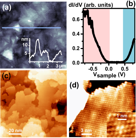
The topography was investigated by atomic force microscopy (AFM) on a m scale and by STM on the nm scale. The AFM topography (Fig. 1(a)) exhibits an overall roughness of 3-4 nmrms due to pyramids with nm in height and a width close to 1 m. On their slopes, atomically flat terraces up to 100 nm in width are found (Fig. 1(c)). These terraces are separated by steps of nm in height, in agreement with the expected Te-Te layer distance of 0.347 nm in cubic GST-225.Nonaka et al. (2000) On the terraces, atomic resolution is achieved by STM (Fig. 1(d)), most likely showing the Te layer.Deringer and Dronskowski (2013) STS shows a band gap of 0.4 eV with situated at the top of the valence band (Fig. 1(b)).
III Results
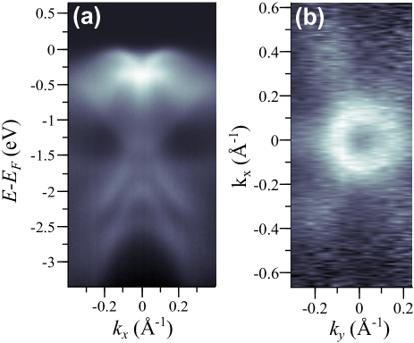
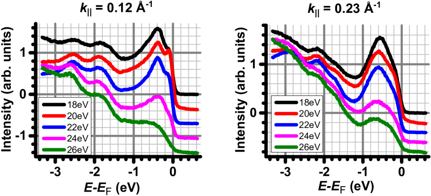
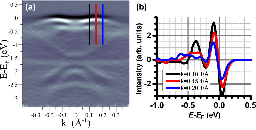
ARPES measurements have been performed at the beamline UE112-lowE-PGM2 () at BESSY II using a Scienta R8000 analyzer. Figure 2(a) displays a spectrum recorded with linearly polarized light at eV in a direction determined to be by comparison with DFT calculations.sup Just below , the upper valence band shows maxima at Å-1 and drops to eV at . Another band resides between -0.7 eV at Å-1 and eV at Å-1. Closer to , these two bands lead to a broad peak in energy distribution curves (EDCs) around eV with a FWHM of eV (Fig. 4(a)). Below eV, there are two more hole-like bands. The direction looks essentially the same with slightly more intensity at even higher values.sup This can be seen from the constant energy cut at in Fig. 2(b), showing a nearly isotropic circle and faint additional intensity at high values in the six different directions.
DFT calculations have been performed within in the generalized gradient approximation.Perdew et al. (1996) We employed the full-potential linearized augmented planewave method in bulk and thin-film geometry Krakauer et al. (1979) as implemented in the FLEUR code.sup Spin-orbit coupling was included self-consistently and a basis set cutoff of was used. As structural model for the cubic phases we adopted the atomic positions given by Sun et al.,Sun et al. (2006) both for the bulk and film structures. For the latter, films consisting of 27 atomic layers terminating by a ’vacancy layer’ were used. Two different stacking sequences were assumed for the cubic phase: a Petrov- and a KH-like sequence which are derived from the respective hexagonal phases by tripling the unit cell and adding appropriate shifts.
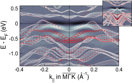
Figure 3 shows the derivative of the measured band structure along with the calculations. A reasonable agreement is only achieved with the Petrov-like stacking, including the minimum at of the upper valence band. The bands further down in energy (around eV at ) can be associated with a Rashba-type surface state, similar to the one observed in Sb2Te3.Pauly et al. (2012) In close vicinity of the upper valence band, the calculation shows the topological surface state crossing the Fermi energy at Å-1. This state obviously overlaps with the upper bulk valence band within our ARPES data.
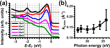
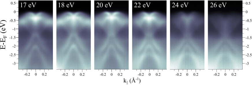
In order to probe different and, thus, distinguish surface from bulk states, spectra with eV have been recorded.sup Corresponding EDCs at are shown in Fig. 4(a). The topmost maximum shifts down by about 0.2 eV between eV and 26 eV, indicating a dispersion, as expected for a band with bulk character. The -position of the VBM has been evaluated by means of the 2nd derivative of the ARPES spectra: the EDC with the peak at the highest energy is chosen, and the corresponding value is taken as .sup Figure 4(b) displays as a function of photon energy revealing a small dependence on as well. Thus, the ARPES peak at the VBM is, at least partially, a bulk band with dispersion in direction.
IV Discussion
The calculated of the bulk valence band ( Å-1) is larger than the experimental one ( Å-1). This can be explained by the overlap with the surface state which crosses at Å-1 (Fig. 3). The small anisotropy of (DFT: 7%, ARPES: <10%) between and was not detectable within the experimental error.
We finally compare the metastable cubic phase with previous DFT calculations of the very similar hexagonal phase. Most notably, a VBM away from consistently indicates topologically non-trivial properties for GST-225.Kim et al. (2010, 2012); Sa et al. (2011, 2012); Silkin et al. (2013) Albeit such a relation is also found for the 3D TIs BiSbHsieh et al. (2008a, b), Bi2Te3Hsieh et al. (2009b); Zhang et al. (2009), and Sb2Te3Hsieh et al. (2009a); Zhang et al. (2009); Pauly et al. (2012), it is currently under discussion for Bi2Se3.Xia et al. (2009); Zhang et al. (2009); Nechaev et al. (2013) None of these materials have a VBM away from with trivial properties.Aguilera et al. (2013) The measured is smaller than the calculated of the bulk VBM of topologically non-trivial hexagonal stable phases of GST-225 ( Å-1).sup The superposition of bulk valence band and topological surface state in the ARPES data might be relevant again.
V Summary
In summary, we have shown by ARPES and STS that metastable cubic Ge2Sb2Te5 epitaxially grown on Si(111) exhibits valence band maxima Å-1 away from and a band gap of 0.4 eV. All DFT calculations of Ge2Sb2Te5 find a VBM away from only for a topological invariant . This implies topological properties of Ge2Sb2Te5, indicates that all phase change materials on the pseudobinary line between Sb2Te3 and Ge2Sb2Te5 are topologically non-trivial, and opens up the possibility of switching between an insulating amorphous phase and a topological phase on ns time scales.
Acknowledgements.
We gratefully acknowledge financial support by the German Science Foundation (DFG): SFB 917, project A3, the SPP 1666 “Topological Insulators” and Mo058/13-1; the Helmholtz-Zentrum Berlin (HZB); the excellence initiative of the German federal government; the Fonds National de la Recherche (Luxembourg). We thank F. Lange, S. Behnke and C. Stemmler for technical support.VI Supplemental Information
VI.1 Sample Preparation
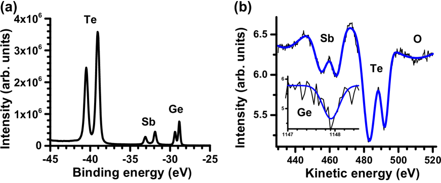
The MBE system, located at the PHARAO beamline at BESSY II (Helmholtz Center for Materials and Energy, Berlin), is equipped with separate dual filament hot lip effusion cells for the evaporation of elemental Ge, Sb, and Te. In-situ reflection high-energy electron diffraction (RHEED), line-of-sight quadrupole mass spectrometry (QMS) and in-situ X-ray diffraction (XRD) by a six-circle diffractometer for synchrotron radiation were used to optimize the growth conditions. After transport under ambient conditions, de-ionized (DI) water dip and annealing in UHV to 250 °C, X-ray photoelectron spectroscopy has been routinely performed in the ARPES chamber. The observed peaks in Fig. 5(a) arise from the Ge 3d, Sb 4d and Te 4d levels.Bearden and Burr (1967); Fuggle and Martensson (1980) The absence of any distortion of the peaks implies a clean and oxygen-free surface. The crystal structure and stoichiometry have been checked after the STM measurements by low-energy electron diffraction (LEED) and Auger electron spectroscopy (AES) (Fig. 5(b)), again after DI water dip and annealing in UHV. The stoichiometry has been calculatedMroczkowski and Lichtman (1985) by using the tabulated sensitivities for Ge, Sb, Te, and O peaks. The larger than stoichiometric Te content of 57% compared to Ge (18%) and Sb (21%) is partly attributed to the Te termination leading to larger AES intensity. Most notably, the oxygen content of the surface is only 4%.
Further heating in vacuum above 300 °C in order to induce a transition into the stable phase at 340 °C,Kooi et al. (2004) was found to cause considerable change in stoichiometry due to the different desorption temperatures of atomic species. At the same time, a change in the peak structures of the Ge 3d and Sb and Te 4d levels in photoelectron spectroscopy was observed. We checked that neither the measurement processes nor our preparation lead to a phase transition. For that purpose, X-ray diffraction after the ARPES measurements was performed showing the same cubic structure with vacancy ordering. Indeed, the power of the incident light of photons/s at eV on a spot area of mm2 can be estimated to be below 3,000 W/m2. Assuming the thermal conductivity of the Si substrate of 150 W/(mK) across the area , a temperature gradient of just 20 K/m, would be enough in order to create a sufficient heat flux. This value is low enough not to induce unintentional heating, or even a phase change of the material.
VI.2 Evaluation of additional ARPES spectra
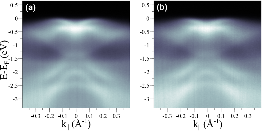
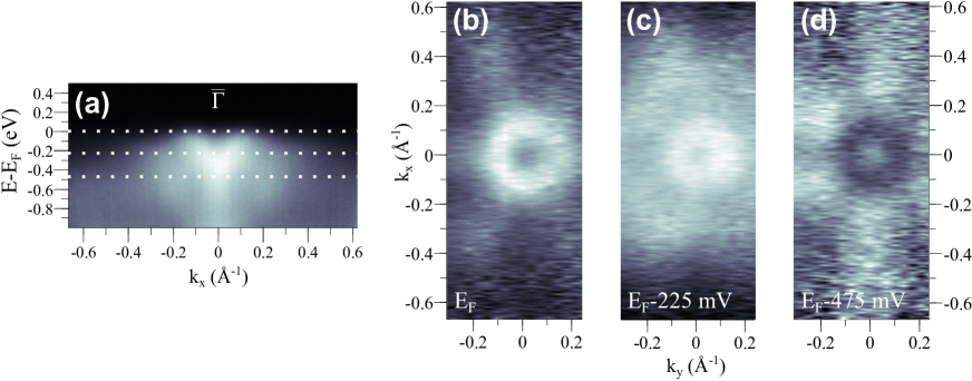
Figure 6 displays two spectra acquired at 22 eV photon energy with 30° relative azimuth rotation in the sample plane. Between them, no difference can be observed at first sight. However, the plots at (Fig. 7(b)-(d)) show a sixfold symmetry at larger values, which persists down to, at least, -220 meV. Since DFT calculations of cubic Ge2Sb2Te5 do not show any bands at higher than Å-1 down to eV in direction, but bands at such high values in (see Fig. 11(b)), we attribute the direction with intensity at high values in Fig. 7(b) to . Thus, we denote Fig. 6(a) as and Fig. 6(b) as . The same assignment is also used in the main text.
The effect of different photon energies is shown in Fig. 8. The upper valence band changes with photon energy revealing itself as a bulk band while the two bands below eV do not. Also in energy distribution curves (Fig. 9), no significant shift of these bands can be observed.
Although the film is in the cubic phase, as deduced from XRD data,Rodenbach et al. (2012a) cuts at different energies as displayed in Fig. 7 show a sixfold symmetry instead of a threefold one. The most probable reason is twinning, i.e., a 180° rotation of crystallographic domains around the surface normal.Rodenbach et al. (2012a) Additionally, it is known from azimuthal XRD scans that the film exhibits rotational domains with a modulated angular spread of °, a behavior typical for epitaxial films of GST,Giussani et al. (2012) Sb2Te3, and GeTeRodenbach et al. (2012b) on Si(111). This twist leads to an angular broadening of the spectra and weakens the measured anisotropy between and directions, thereby making a better agreement of an untwinned film with the calculations of the bulk VBM more likely.
The energy distribution curves in Fig. 9 show the development of the upper valence band at higher with photon energy, again indicating the bulk-like character by the observable dispersion.
VI.3 Determination and comparison of valence band maxima
The maximum of the valence band has been determined for different photon energies by means of the second derivative of the ARPES intensity with respect to electron energy. Figure 10 shows an example of the evaluation procedure. After computing the second derivative (Fig. 10(a)), energy distribution curves (EDCs) of these data along constant are extracted. The peak being closest to the Fermi energy marks the energy of the valence band at the given . For determination of the value of the valence band maximum (VBM), EDCs for different are evaluated and the where the valence band peak is highest in energy is taken as the position of the VBM, . This procedure is applied for the ARPES spectra of 6 different photon energies (Fig. 8) and entered into Fig. 4(b) of the main text. Since only EDCs at constant are used, variations in ARPES intensity with detection angle, or , do not influence the outcome.
| this work | Kim et al.111see Ref. Kim et al., 2010 | Silkin et al.222see Ref. Silkin et al., 2013 | ||||
| cubic | Petrov | 25% | 50% | |||
| (DFT) | 0.19 | 0.18 | 0.29 | 0.30 | ||
| (DFT) | 0.22 | 0.26 | 0.51 | 0.52 | ||
| eV (exp., ) | 0.14 | 0.18 | 0.20 | 0.16 | ||
| eV (exp., ) | 0.18 | 0.21 | 0.25 | 0.21 | ||
Table 1 compares the experimental values of the VBM to calculations of the hexagonal stable phase and the cubic metastable phase. Best agreement is found with the slab calculation of the Petrov phaseKim et al. (2010) and with the mixed phase with equal distribution of Ge and Sb ().Silkin et al. (2013) Within the Brillouin zone of this phase, , the valence band maximum projected onto the (0001) plane, is closest to at the edge of the Brillouin zone (see cuts connecting the points in Ref. Silkin et al., 2013).
VI.4 Density functional theory calculations of the metastable phase
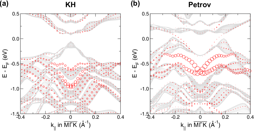
Density functional theory calculations including spin-orbit coupling have been employed using the FLEUR codefla for the metastable cubic phase of GST-225. The structure has been derived from the hexagonal KH and Petrov phase by introducing a shift of one part of the unit cell within the [0001] plane, as proposed by Sun et al. in Ref. Sun et al., 2006. The results qualitatively agree with the calculations of the hexagonal phaseKim et al. (2010); Silkin et al. (2013) in that a VBM away from and a topological surface state is found for the Petrov-type stacking and a VBM at and no topological surface state for the KH-type stacking. The topological surface state in the Petrov phase crosses at lower than that of the VBM. The KH phase exhibits a VBM at for all while the Petrov phase shows the VBM away from for all in accordance with the ARPES data. The strongest surface character is found for the Rashba-type surface state at eV at similar to the case of Sb2Te3.Pauly et al. (2012)
References
- Volkov and Pankratov (1985) B. A. Volkov and O. A. Pankratov, JETP Lett. 42, 178 (1985).
- Fu et al. (2007) L. Fu, C. L. Kane, and E. J. Mele, Phys. Rev. Lett. 98, 106803 (2007).
- König et al. (2007) M. König, S. Wiedmann, C. Brüne, A. Roth, H. Buhmann, L. W. Molenkamp, X.-L. Qi, and S.-C. Zhang, Science 318, 766 (2007).
- Hsieh et al. (2008a) D. Hsieh, D. Qian, L. Wray, Y. Xia, Y. S. Hor, R. J. Cava, and M. Z. Hasan, Nature 452, 970 (2008a).
- Eremeev et al. (2012) S. V. Eremeev, G. Landolt, T. V. Menshchikova, B. Slomski, Y. M. Koroteev, Z. S. Aliev, M. B. Babanly, J. Henk, A. Ernst, L. Patthey, et al., Nat. Commun. 3, 635 (2012).
- Ando (2013) Y. Ando, arXiv:1304.5693v2 (2013).
- Wuttig and Yamada (2007) M. Wuttig and N. Yamada, Nat. Mater. 6, 824 (2007).
- Wuttig and Raoux (2012) M. Wuttig and S. Raoux, Z. Anorg. Allg. Chem. 638, 2455 (2012).
- Lencer et al. (2008) D. Lencer, M. Salinga, B. Grabowski, T. Hickel, J. Neugebauer, and M. Wuttig, Nat. Mater. 7, 972 (2008).
- Ovshinsky (1968) S. R. Ovshinsky, Phys. Rev. Lett. 21, 1450 (1968).
- Yamada et al. (1987) N. Yamada, E. Ohno, N. Akahira, K. Nishiuchi, K. Nagata, and M. Takao, J. Appl. Phys. 26, 61 (1987).
- Yamada et al. (1991) N. Yamada, E. Ohno, K. Nishiuchi, N. Akahira, and M. Takao, J. Appl. Phys. 69, 2849 (1991).
- Loke et al. (2012) D. Loke, T. H. Lee, W. J. Wang, L. P. Shi, R. Zhao, Y. C. Yeo, T. C. Chong, and S. R. Elliott, Science 336, 1566 (2012).
- Xiong et al. (2011) F. Xiong, A. D. Liao, D. Estrada, and E. Pop, Science 332, 568 (2011).
- Hsieh et al. (2009a) D. Hsieh, Y. Xia, D. Qian, L. Wray, F. Meier, J. H. Dil, J. Osterwalder, L. Patthey, A. V. Fedorov, H. Lin, et al., Phys. Rev. Lett. 103, 146401 (2009a).
- Zhang et al. (2009) H. Zhang, C.-X. Liu, X.-L. Qi, X. Dai, Z. Fang, and S.-C. Zhang, Nat. Phys. 5, 438 (2009).
- Pauly et al. (2012) C. Pauly, G. Bihlmayer, M. Liebmann, M. Grob, A. Georgi, D. Subramaniam, M. R. Scholz, J. Sanchez-Barriga, A. Varykhalov, S. Blügel, et al., Phys. Rev. B 86, 235106 (2012).
- Kim et al. (2010) J. Kim, J. Kim, and S.-H. Jhi, Phys. Rev. B 82, 201312 (2010).
- Kim et al. (2012) J. Kim, J. Kim, K.-S. Kim, and S.-H. Jhi, Phys. Rev. Lett. 109, 146601 (2012).
- Kim and Jhi (2012) J. Kim and S.-H. Jhi, Phys. Status Solidi B 249, 1874 (2012).
- Silkin et al. (2013) I. V. Silkin, Y. M. Koroteev, G. Bihlmayer, and E. V. Chulkov, Appl. Surf. Sci. 267, 169 (2013).
- Park et al. (2007) J.-B. Park, G.-S. Park, H.-S. Baik, J.-H. Lee, H. Jeong, and K. Kim, J. Electrochem. Soc. 154, H139 (2007).
- Petrov et al. (1968) I. I. Petrov, R. M. Imamov, and Z. G. Pinsker, Sov. Phys. Crystallogr. 13, 339 (1968).
- Kooi and Hosson (2002) B. J. Kooi and J. T. M. D. Hosson, J. Appl. Phys. 92, 3584 (2002).
- Sun et al. (2006) Z. Sun, J. Zhou, and R. Ahuja, Phys. Rev. Lett 96, 055507 (2006).
- Matsunaga et al. (2004) T. Matsunaga, N. Yamada, and Y. Kubota, Acta Crystallogr. B 60, 685 (2004).
- Yamada and Matsunaga (2000) N. Yamada and T. Matsunaga, J. Appl. Phys. 88, 7020 (2000).
- Park et al. (2005) Y. J. Park, J. Y. Lee, M. S. Youm, Y. T. Kim, and H. S. Lee, J. Appl. Phys. 97, 093506 (2005).
- Sa et al. (2011) B. Sa, J. Zhou, Z. Song, Z. Sun, and R. Ahuja, Phys. Rev. B 84, 085130 (2011).
- Sa et al. (2012) B. Sa, J. Zhou, Z. Sun, and R. Ahuja, Europhys. Lett. 97, 27003 (2012).
- Katmis et al. (2011) F. Katmis, R. Calarco, K. Perumal, P. Rodenbach, A. Giussani, M. Hanke, A. Proessdorf, A. Trampert, F. Grosse, R. Shayduk, et al., Cryst. Growth & Design 11, 4606 (2011).
- Rodenbach et al. (2012a) P. Rodenbach, R. Calarco, K. Perumal, F. Katmis, M. Hanke, A. Proessdorf, W. Braun, A. Giussani, A. Trampert, H. Riechert, et al., Phys. Status Solidi-RRL 6, 415 (2012a).
- Takagaki et al. (2012) Y. Takagaki, A. Giussani, K. Perumal, R. Calarco, and K.-J. Friedland, Phys. Rev. B 86, 125137 (2012).
- Giussani et al. (2012) A. Giussani, K. Perumal, M. Hanke, P. Rodenbach, H. Riechert, and R. Calarco, Phys. Status Solidi B 249, 1939 (2012).
- Takagaki et al. (2013) Y. Takagaki, A. Giussani, J. Tominaga, U. Jahn, and R. Calarco, J. Phys.-Condens. Mat. 25, 345801 (2013).
- (36) See supplementary material at [URL] for further information on sample preparation, crystallographic directions, additional ARPES spectra, and calculations.
- Zhang et al. (2010) Z. Zhang, J. Pan, Y. L. Foo, L. W.-W. Fang, Y.-C. Yeo, R. Zhao, L. Shi, and T.-C. Chong, Appl. Surf. Sci. 256, 7696 (2010).
- Nonaka et al. (2000) T. Nonaka, G. Ohbayashi, Y. Toriumi, Y. Mori, and H. Hashimoto, Thin Solid Films 370, 258 (2000).
- Deringer and Dronskowski (2013) V. L. Deringer and R. Dronskowski, J. Phys. Chem. C 117, 15075 (2013).
- Perdew et al. (1996) J. P. Perdew, K.Burke, and M. Ernzerhof, Phys. Rev. Lett. 77, 3865 (1996).
- Krakauer et al. (1979) H. Krakauer, M. Posternak, and A. J. Freeman, Phys. Rev. B 19, 1706 (1979).
- Hsieh et al. (2008b) D. Hsieh, Y. Xia, L. Wray, D. Qian, A. Pal, J. H. Dil, J. Osterwalder, F. Meier, G. Bihlmayer, C. L. Kane, et al., Science 323, 919 (2008b).
- Hsieh et al. (2009b) D. Hsieh, Y. Xia, D. Qian, L. Wray, J. H. Dil, F. Meier, J. Osterwalder, L. Patthey, J. G. Checkelsky, N. P. Ong, et al., Nature 460, 1101 (2009b).
- Xia et al. (2009) Y. Xia, D. Qian, D. Hsieh, L. Wray, A. Pal, H. Lin, A. Bansil, D. Grauer, Y. S. Hor, R. J. Cava, et al., Nat. Phys. 5, 398 (2009).
- Nechaev et al. (2013) I. A. Nechaev, R. C. Hatch, M. Bianchi, D. Guan, C. Friedrich, I. Aguilera, J. L. Mi, B. B. Iversen, S. Blügel, P. Hofmann, et al., Phys. Rev. B 87, 121111 (2013).
- Aguilera et al. (2013) I. Aguilera, C. Friedrich, G. Bihlmayer, and S. Blügel, Phys. Rev. B 88, 045206 (2013).
- Bearden and Burr (1967) J. A. Bearden and A. F. Burr, Rev. Mod. Phys. 39, 125 (1967).
- Fuggle and Martensson (1980) J. G. Fuggle and N. Martensson, J. Electron. Spectrosc. Relat. Phenom. 21, 275 (1980).
- Mroczkowski and Lichtman (1985) S. Mroczkowski and D. Lichtman, J. Vac. Sci. Technol. A 3, 1860 (1985).
- Kooi et al. (2004) B. J. Kooi, W. M. G. Groot, and J. T. M. D. Hosson, J. Appl. Phys. 95, 924 (2004).
- Rodenbach et al. (2012b) P. Rodenbach, A. Giussani, K. Perumal, M. Hanke, M. Dubslaff, H. Riechert, R. Calarco, M. Burghammer, A. V. Kolobov, and P. Fons, Appl. Phys. Lett. 101, 061903 (2012b).
- (52) For a program description see http://www.flapw.de.