A diffraction effect in X-ray area detectors
Abstract
When an X-ray area detector based on a single crystalline material, for instance, a state of the art hybrid pixel detector, is illuminated from a point source by monochromatic radiation, a pattern of lines appears which overlays the detected image. These lines can be easily found by scattering experiments with smooth patterns, such as small-angle X-ray scattering. The origin of this effect is the Bragg reflection in the sensor layer of the detector. Experimental images are presented over a photon energy range from 3.4 keV to 10 keV, together with a theoretical analysis. The intensity of this pattern is up to , which can disturb the evaluation of scattering and diffraction experiments. The patterns can be exploited to check the alignment of the detector surface with the direct beam, and the alignment of individual detector modules with each other in the case of modular detectors, as well as for the energy calibration of the radiation.
I Introduction
Images of X-ray scattering and diffraction experiments are typically recorded nowadays by using a large-area digital detector. The recent advances of so-called hybrid pixel detectors, where an electronic circuit board is bump bonded to a sensor layer Heijne and Jarron (1989), have improved the image quality to a large extent. State-of-the art detectors like the XPAD Delpierre et al. (2007), detectors based on the Medipix read-out chip Ponchut et al. (2002); Pennicard et al. (2010), and the PILATUS Kraft et al. (2009); Donath et al. (2013) combine a pixelated semiconductor sensor with a circuit board providing an amplifier, a discriminator and a digital counter for every single pixel. By means of this technique, the detector directly counts single X-ray photons for every pixel, and the image quality in terms of the signal-to-noise ratio is ultimately only limited by the quantum noise of the photons. In addition, large dynamic ranges and very small crosstalk between neighbouring pixels can be achieved.
The sensitive layer of such a detector, which absorbs the photons and converts them into an electric signal, is usually made of a single crystal silicon wafer, but CdTe or CdZnTe sensors are also in use for detectors operating in the keV to keV photon energy range Takahashi and Watanabe (2001).
Mostly, the crystalline structure of the sensor layer of the detector is of minor importance to the primary scattering experiment. However, Bragg reflection in this layer, which is characteristic of a crystalline material, can significantly change the detected signal. This was shown by Zheludeva et al. (1985) for a photodiode point detector and by Holý et al. (1985), who measured the photoconductivity of the second crystal in a double-crystal monochromator as a function of the angle. The strong angular and energy dependency of the detected signal as a result of the Bragg diffraction was first exploited by Jach et al. (1988), who embedded a photodiode directly in the monochromator crystal to assist in tuning the crystals Jach (1990). Later, Erko et al. (2001) and Krumrey and Ulm (2001) used the effect in an external photodiode to calibrate the energy scale of their X-ray monochromators. Hönnicke et al. (2004) implemented it as a novel method to detect a diffracted beam at an angle of 90°.
Hönnicke and Cusatis (2005) extended the idea of Jach et al. (1988) by using a CCD as a monochromator crystal to simultaneously monochromatize the incoming X-rays and detect a spatially resolved image. They observed a dark curved line across the detected image which depends on the photon energy and the angle of incidence and indicates the position on the crystal at which the Bragg condition is fulfilled.
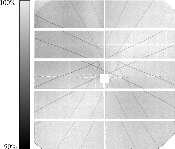
A similar pattern can arise in every diffraction experiment, when a single crystalline imaging detector is used. In this paper, regular patterns in the detected images of a photon-counting hybrid pixel detector are reported which are caused by elastic Bragg scattering in the sensor layer of the detector. Figure 1 displays an example image recorded by a homogeneously illuminated detector. The image was high-pass filtered to enhance the visibility of the pattern using the procedure described in detail later in this paper. Ideally, this image would be completely featureless, but the Bragg pattern overlays the detected image in the form of faint dark lines. When the energy is changed, the lines move across the entire image and finally disappear when they move out of the detector area.
These artefacts are always present when the detector is illuminated by monochromatic radiation from a point source, which is the typical configuration for many scattering and diffraction experiments. However, for primary signals with a large variation in contrast and small-scale features such as crystallography diffraction images, the patterns may go unnoticed. They are most easily observed for small-angle scattering (SAXS) experiments which can lead to smooth scattering patterns.
The formation of these patterns can be explained as follows: at every detector pixel, the angle of incidence of the incoming photons is different in the crystalline coordinate system. At some point, the incident photon may fulfill the Bragg condition of an arbitrary symmetry plane. This photon has a finite probability to be elastically reflected out of the sensor layer, and consequently is not measured. This leads to a lower signal of the detector at the corresponding pixel, and possibly a higher signal at a nearby pixel, if the photon is still absorbed inside the detector. The mechanics of losing a photon due to parasitic Bragg scattering resembles the well-known monochromator glitches Laan and Thole (1988). When the photon energy is fixed, the Bragg condition still leaves one degree of freedom for the incident direction, namely the rotational symmetry about the normal vector of the Bragg plane. It follows that the pattern consists of lines.
This paper is organized as follows. First, the experiments are described in detail. Then a theoretical analysis of the patterns is given based on Bragg diffraction. Next, the experimentally observed images are compared with the theoretical predictions and finally possible applications of the phenomenon are discussed.
II Experiments and data processing
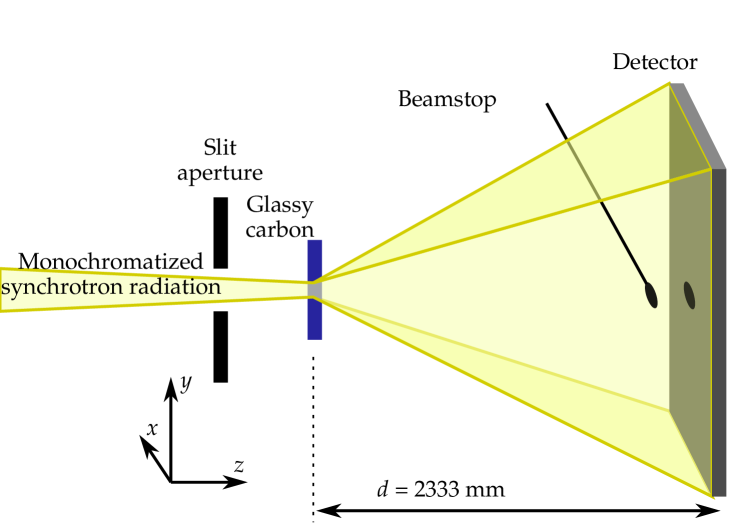
The experimental setup is illustrated in figure 2. It is based on a common small-angle X-ray scattering setup at the synchrotron radiation facility BESSY II at the FCM beamline Krumrey (1998); Krumrey and Ulm (2001). The radiation from a bending magnet is monochromatized using a four-crystal monochromator equipped with InSb(111) and Si(111) crystals, which provides an energy range from keV to keV. The monochromatized radiation is then collimated using a slit aperture of the size and focused on the sample. The key point in observing the patterns is the selection of a sample which scatters uniformly over the whole detector area. For the energy range from to , a thick sample of glassy carbon was used, and below , a sample of the same material with a thickness of µm was used. Glassy carbon is a common reference material in SAXS due to its low variation in scattering intensity over the range of the momentum transfer between and Zhang et al. (2010), making it an ideal scatterer to provide a nearly homogeneous illumination.
The scattered radiation is then collected by a PILATUS 1M detector from Dectris Ltd., modified for direct operation in vacuum Donath et al. (2013); Wernecke et al. (2013). This detector consists of ten modules, each of which contains photon counting pixels with a pixel size of µm. The sensor layer of each module is made of a silicon wafer with the plane facing the beam. The long side of the module is parallel to the axis of the wafer, which corresponds to the detector -axis. This detector is mounted on the SAXS setup of the Helmholtz-Zentrum Berlin Krumrey et al. (2011), which allows positioning with µm resolution along the beam ( axis in figure 2) and perpendicular to it ( and axes). The sample-detector distance was set to for all experiments.
The images were subsequently filtered using the following procedure to enhance the visibility of the patterns. First, an azimuthal averaging is performed, which is a standard preprocessing step for SAXS data Pauw (2013). During this processing, all pixels which deviate by more than 3 standard deviations from the median intensity are treated as outliers and are excluded. Then, the original data is divided by the resulting scattering curve pixel by pixel. This results in an image of the relative deviation of every pixel from the mean value for the corresponding . This processing acts as a (non-linear) high-pass filter with the corresponding low pass defined by the azimuthal averaging step. Finally, the contrast range of the image is adjusted for visualization. A range of to of the full scale intensity is suitable for most of the patterns.
The image in figure 1 was processed in this way to clearly display the pattern. The raw image varies in intensity by more than a factor of 3 from the centre to the border, because the scattering from glassy carbon is not perfectly isotropic. The pattern, on the other hand, changes the intensity by only and is hard to detect by eye when the full dynamic range of the image is displayed. The filter makes the pattern easily visible across the whole image and the full energy range by removing the background.
Some regions of the original image have been masked after the processing. This includes the beamstop, together with the mounting parts, the gaps between the individual detector modules, and areas shadowed by elements of the beamline. These areas are marked in the filtered images in white.
III Theory
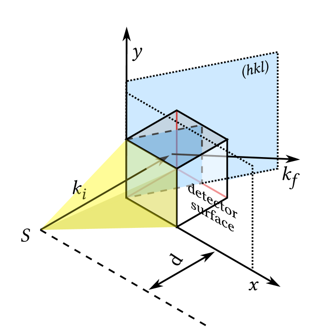
The geometry of the problem is depicted in figure 3. The detector is illuminated from a monochromatic point source located at at a distance from the surface. Consider a crystallographic plane with the Miller indices , which is generally not parallel to the detector surface. A pattern line can appear at every position at the surface, where the incident photon with the wave vector fulfills the Bragg condition
| (1) |
where is the reciprocal lattice vector of the corresponding plane. With the coordinates of the intersection of the detector surface and the ray, the wave vector can be expressed in the experimental frame as
| (2) |
where is the wavelength of the photon. In order to substitute (2) into (1), the wave vector must be transformed into the crystalline coordinate system. In this case the detector surface was parallel to the crystallographic plane , and the detector -axis was parallel to the unit vector of the cubic lattice, which defines the coordinates of any point on the surface as
| (3) | ||||
Substituting the transformed coordinates into the Laue equation (1) yields the implicit function
| (4) |
where is the lattice constant of the cubic lattice.
The solution to this equation in the unknowns describes the expected patterns resulting from diffraction at the plane . Since the Bragg angle is invariant under the exchange of and and sign change, one has to respect all these permutations when solving the condition (4). This explains the 8-fold symmetry of the patterns observed (cf. figure 1). If either or is zero, or , the symmetry collapses into a 4-fold pattern. If both and are zero, equation (4) describes a circle with the radius
| (5) |
Generally, equation (4) can be rearranged into a quadratic polynomial over the detector coordinates . Thus, all the lines represent conic sections.
For a given set of indices , a characteristic wavelength or photon energy can be defined where all lines of a specific pattern meet in the detector centre, at which point the incident photon angle is normal to the detector surface. The condition for this characteristic energy is given by substituting into equation (4) and solving for the energy
| (6) |
In the case of the circular pattern, the condition (4) can only be fulfilled for photon energies above , at which the pattern consists of a singular point in the detector centre.
In the next section, the numerical solutions to (4) will be compared to the experimental findings.
IV Results and Discussion
| (eV) | Intensity | Symmetry | |||
|---|---|---|---|---|---|
| 1 | 1 | 1 | 3424.29 | ||
| 1 | 1 | 3 | 4185.25 | ||
| 2 | 0 | 2 | 4565.73 | ||
| 0 | 0 | 4 | 4565.73 | ||
| 1 | 1 | 5 | 6163.73 | ||
| 2 | 2 | 4 | 6848.59 | ||
| 3 | 1 | 3 | 7229.06 | ||
| 2 | 0 | 6 | 7609.54 | ||
| 3 | 1 | 5 | 7990.02 | ||
| 1 | 1 | 7 | 8316.14 | ||
| 4 | 0 | 4 | 9131.45 | ||
| 0 | 0 | 8 | 9131.45 | ||
| 3 | 1 | 7 | 9620.63 | ||
| 3 | 3 | 5 | 9816.31 |
Three different sets of scattering images from glassy carbon were recorded over the range from keV to keV. The first set comprises an image at each of the characteristic energies listed in table 1. The second set of images was recorded in steps of eV over a photon energy range from keV to keV. The last set of images comprises a sequence in steps of and at about the characteristic energies of the circular patterns and , respectively.
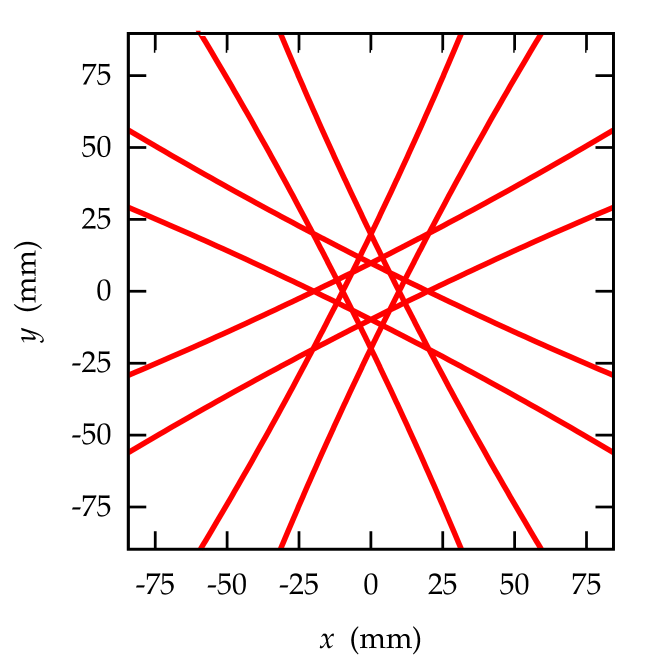
The filtered images are then compared to the numerical solution of equation (4). A simulation corresponding to the experimental frame in figure 1 is shown in figure 4. The photon energy, the distance and the detector area were chosen from the experimental conditions. The value of the silicon lattice constant was taken from Mohr et al. (2012) and corrected for thermal expansion to using the data from Swenson (1983). The Miller indices were set to , and this results in a pattern with striking similarity to the experimental image. It is impossible to fulfill the Bragg condition for any other combination of indices in the considered range at the given photon energy.
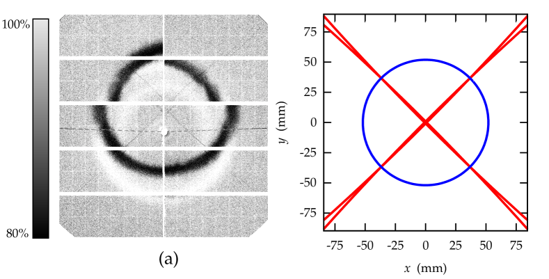
A comparison of simulated and experimental data at a selection of the characteristic energies in the experimentally covered photon energy range is shown in figure 5. The possible patterns fall into four categories, each of which is represented by one image in figure 5. When both (figure 5a), the expected pattern is a circle with the centre at the point of normal incidence, which has been discussed already in section III. This image was taken at eV above the characteristic energy, because the circular pattern exists only for . For even larger energies, the pattern will be outside the detector area. This demonstrates the strong sensitivity of the patterns to the photon energy.
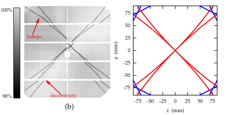
When and , the lines are oriented parallel to the crystalline coordinate system. For a detector with the -axis parallel to , this results in a diagonal cross, as shown in figure 5b. A much weaker pattern of the same type is also present in figure 5a, which comes from the plane.
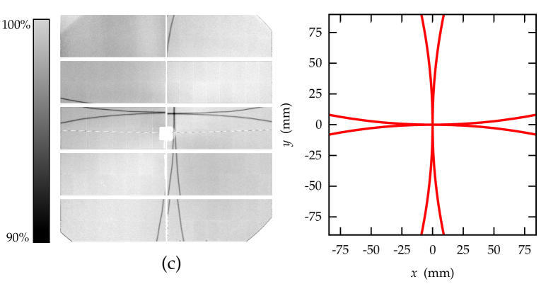
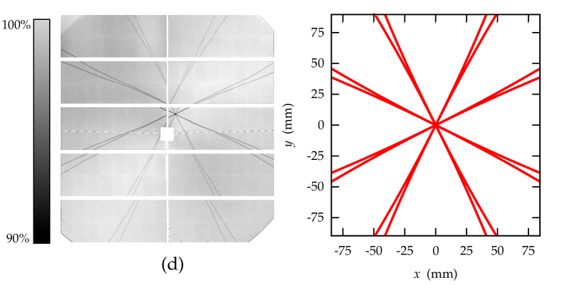
For , the resulting 4-fold symmetry is oriented along the direction, which displays an upright cross (figure 5c). Finally, in the general case , an 8-fold symmetry is observed (figure 5d). All patterns predicted in table 1 have been experimentally confirmed up to a photon energy of .
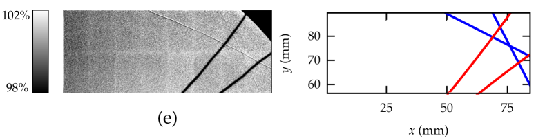
The measured intensities of the patterns (see table 1) vary greatly from pattern to pattern. Most of the patterns lead to a decrease in the intensity of the pixels on the line with respect to the undistorted signal. An increase in the line intensity with respect to the surroundings could only be observed for the pattern coming from the plane, and the patterns caused by reflections at the and planes display a double line with lower and higher intensity side by side (see figure 5e for an example). The former can be explained by reabsorption of the scattered photons in the same pixel, where the reflection occurs, which improves the absorbance and thus the quantum efficiency of the detector. The latter is explained by the reabsorption of the reflected photons in a nearby pixel, thus transferring the measured signal from the dark to the bright pattern line.
While the strongest pattern, for instance the circle, leads to a intensity decrease compared to the undistorted signal, some of the weakest lines approach only a decrease by , as listed in table 1. These intensities significantly exceed the noise even for moderate count rates, and may therefore impede the data evaluation for applications such as protein crystallography Usón and Sheldrick (1999), if the existence of the pattern is neglected. A quantitative theoretical analysis of the line intensities, which requires a space-resolved dynamical scattering theory, is beyond the scope of this paper.
The prediction of the theory is accurate in terms of the energy scale. This can be concluded from the figures 5b, c and d, where the photon energy of the exposures is off by less than from the true characteristic energy. The pattern lines meet at one point, as predicted by equation (6). Therefore the computed characteristic energies agree with the experimentally determined intersection points of the patterns up to the energy resolution of the monochromator of around .
Despite the good agreement in terms of the energy scale, there are some differences when the pattern is compared to the simulations in detail, which are marked with arrows in figure 5b. First, large discontinuities disrupt the pattern across the gap between individual modules. This artefact is especially prominent between the two lowest rows in figure 5b. Second, the lines are not ideally smooth, but display bumps, especially prominent in the top row of figure 5b. The discontinuities arise most probably from an imperfect alignment of the modules with respect to each other. The angular sensitivity of the pattern can be estimated from the width of the lines, which is approximately arc seconds corresponding to in the given setup. Therefore, even the slightest angular deviation manifests itself as a shift in the pattern. Another possible reason is the imperfect orientation of the sensor surface with respect to the crystalline coordinate system, which may vary between individual modules. Similarly, the bumps in the lines probably come from the roughness of the detector surface. This roughness may stem from either the production process of the silicon wafer or from mechanical stress in the wafer, which is permanently bump-bonded to the supporting circuitry. It should be noted that the deviations visible here are only observed in the Bragg line pattern and not in the primary scattering image, which is rather insensitive to the angular misalignment.
V Potential Applications
Due to the sensitivity of the Bragg line patterns to the energy and angle of incidence, a number of applications can be considered. It is straightforward to check the energy calibration of the monochromator with the aid of the characteristic energies . When the photon energy is set to one of the characteristic energies, which are well distributed in a large range (see table 1), all the lines must meet at one point. If this is not the case, the sign of the deviation can be concluded from the curvature of the lines. When the inner polygon formed by the lines is concave, the photon energy is below the characteristic energy, and vice versa, for a convex inner polygon. This follows from the fact that the radius of the curved lines increases with the energy. In principle, this method even allows measurement of the energy over a certain range in the neighbourhood of , by determining the area of the inner polygon. For conclusive results, however, it is necessary to know the distance from the source, which may limit the accuracy.
Another possible application is the determination of the angular alignment. The point at which the lines meet, i.e. the normal incidence on the detector plane, should coincide with the direct beam for a perfectly aligned detector. In the experimental data shown in section IV, this is clearly not the case. However, the distance of the pattern centre from the direct beam position is only , which corresponds to an angular misalignment of °. For the application of recording scattering images, this is negligible, since the cosine of this angle differs by only one part in from unity. The discontinuity of the pattern across module borders and the height of the line bumps can be evaluated in a similar way to compute the angle between individual modules and the roughness of the detector surface. The result is of a similar scale, and thus the deviations are too small to be observed in regular scattering images.
VI Conclusion
A line pattern in X-ray detector images has been discovered which results from Bragg scattering in the sensor layer of the detector. The pattern overlays all images recorded in typical small-angle scattering geometry when the sensor layer of the detector is made of crystalline material, which is the case for all state-of-the-art hybrid pixel detectors. The intensity of this pattern is sufficient to disturb the evaluation of scattering and diffraction experiments. First theoretical considerations can explain the observed patterns with perfect agreement in the investigated photon energy range. The effect can be exploited to accurately measure the photon energy and the angular alignment of the detector with the primary beam.
Acknowledgements.
The experimental contributions from Stefanie Marggraf and Levent Cibik are gratefully acknowledged. We thank Frank Scholze and Jan Wernecke for interesting discussions. We would also like to thank Armin Hoell for the research cooperation with the HZB SAXS instrument as well as DECTRIS for providing data and support with the PILATUS detector.References
- Delpierre et al. (2007) Delpierre, P., S. Basolo, J.-F. Berar, M. Bordesoule, N. Boudet, P. Breugnon, B. Caillot, B. Chantepie, J. Clemens, B. Dinkespiler, S. Hustache-Ottini, C. Meessen, M. Menouni, C. Morel, C. Mouget, P. Pangaud, R. Potheau, and E. Vigeolas (2007), Nucl. Instr. Meth. A 572, 250.
- Donath et al. (2013) Donath, T., S. Brandstetter, L. Cibik, S. Commichau, P. Hofer, M. Krumrey, B. Lüthi, S. Marggraf, P. Müller, M. Schneebeli, C. Schulze-Briese, and J. Wernecke (2013), J. Phys.: Conf. Ser. 425, 062001.
- Erko et al. (2001) Erko, A., I. Packe, W. Gudat, N. Abrosimov, and A. Firsov (2001), Nucl. Instr. Meth. A 467, 623.
- Heijne and Jarron (1989) Heijne, E. H., and P. Jarron (1989), Nucl. Instr. Meth. A 275, 467.
- Holý et al. (1985) Holý, V., J. Hlávka, and J. Kuběna (1985), Phys. Status Solidi A 90, K87.
- Hönnicke and Cusatis (2005) Hönnicke, M., and C. Cusatis (2005), J. Phys. D: Appl. Phys. 38, A73.
- Hönnicke et al. (2004) Hönnicke, M. G., E. M. Kakuno, C. Cusatis, and I. Mazzaro (2004), J. Appl. Cryst. 37, 451.
- Jach (1990) Jach, T. (1990), Nucl. Instr. Meth. A 299, 76.
- Jach et al. (1988) Jach, T., D. Novotny, G. Carver, J. Geist, and R. Spal (1988), Nucl. Instr. Meth. A 263, 522.
- Kraft et al. (2009) Kraft, P., A. Bergamaschi, C. Broennimann, R. Dinapoli, E. Eikenberry, B. Henrich, I. Johnson, A. Mozzanica, C. Schlepütz, P. Willmott, and B. Schmitt (2009), J. Synchrotron Rad. 16, 368.
- Krumrey (1998) Krumrey, M. (1998), J. Synchrotron Rad. 5, 6.
- Krumrey et al. (2011) Krumrey, M., G. Gleber, F. Scholze, and J. Wernecke (2011), Meas. Sci. Technol. 22, 094032.
- Krumrey and Ulm (2001) Krumrey, M., and G. Ulm (2001), Nucl. Instr. Meth. A 467-468, 1175.
- Laan and Thole (1988) Laan, G. V. D., and B. T. Thole (1988), Nucl. Instr. Meth. A 263, 515.
- Mohr et al. (2012) Mohr, P. J., B. N. Taylor, and D. B. Newell (2012), Rev. Mod. Phys. 84, 1527.
- Pauw (2013) Pauw, B. R. (2013), J. Phys.: Condens. Matter 25, 383201.
- Pennicard et al. (2010) Pennicard, D., J. Marchal, C. Fleta, G. Pellegrini, M. Lozano, C. Parkes, N. Tartoni, D. Barnett, I. Dolbnya, K. Sawhney, R. Bates, V. O’Shea, and V. Wright (2010), IEEE Trans. Nucl. Sci. 57, 387.
- Ponchut et al. (2002) Ponchut, C., J. Visschers, A. Fornaini, H. Graafsma, M. Maiorino, G. Mettivier, and D. Calvet (2002), Nucl. Instr. Meth. A 484, 396.
- Swenson (1983) Swenson, C. A. (1983), J. Phys. Chem. Ref. Data 12, 179.
- Takahashi and Watanabe (2001) Takahashi, T., and S. Watanabe (2001), IEEE Trans. Nucl. Sci. 48, 950.
- Usón and Sheldrick (1999) Usón, I., and G. M. Sheldrick (1999), Curr. Opin. Struct. Biol. 9, 643.
- Wernecke et al. (2013) Wernecke, J., C. Gollwitzer, P. Müller, and M. Krumrey (2013), J. Instrum. In preparation.
- Zhang et al. (2010) Zhang, F., J. Ilavsky, G. G. Long, J. P. Quintana, A. J. Allen, and P. R. Jemian (2010), Metall. Mater. Trans. A 41, 1151.
- Zheludeva et al. (1985) Zheludeva, S. I., M. V. Kovalchuk, and V. G. Kohn (1985), J. Phys. C: Solid State 18, 2287.