preprint
This is an updated version of our article, due to be published in Contemporary Physics (Sept 2013). Included are updated references, along with a few minor corrections.
Introduction to Graphene Electronics – A New Era of Digital Transistors and Devices
Abstract
The speed of silicon-based transistors has reached an impasse in the recent decade, primarily due to scaling techniques and the short-channel effect. Conversely, graphene (a revolutionary new material possessing an atomic thickness) has been shown to exhibit a promising value for electrical conductivity. Graphene would thus appear to alleviate some of the drawbacks associated with silicon-based transistors. It is for this reason why such a material is considered one of the most prominent candidates to replace silicon within nano-scale transistors. The major crux here, is that graphene is intrinsically gapless, and yet, transistors require a band-gap pertaining to a well-defined ON/OFF logical state. Therefore, exactly as to how one would create this band-gap in graphene allotropes is an intensive area of growing research. Existing methods include nano-ribbons, bilayer and multi-layer structures, carbon nanotubes, as well as the usage of the graphene substrates. Graphene transistors can generally be classified according to two working principles. The first is that a single graphene layer, nanoribbon or carbon nanotube can act as a transistor channel, with current being transported along the horizontal axis. The second mechanism is regarded as tunneling, whether this be band-to-band on a single graphene layer, or vertically between adjacent graphene layers. The high-frequency graphene amplifier is another talking point in recent research, since it does not require a clear ON/OFF state, as with logical electronics. This paper reviews both the physical properties and manufacturing methodologies of graphene, as well as graphene-based electronic devices, transistors, and high-frequency amplifiers from past to present studies. Finally, we provide possible perspectives with regards to future developments.
I Introduction
Not long before graphene was first manufactured by the Manchester research group in 2004 Novoselov1 ; Geim1 ; Geim2 ; Geim3 , theorists still believed that such two-dimensional structures were unstable due to thermal fluctuations Geim3 ; Meyer , famously referred to as the Landau–Peierls arguments (cf. also Mermin–Wagner theorem Meyer ; O'Hare ; O'Hare1 ). Recently, the paradox behind graphene’s existence has been resolved Meyer ; O'Hare , and that it can be stabilised by transverse lattice distortions Tapaszto . Stable forms of various other two-dimensional crystals such as graphene, silicene and germanene have all been attained O'Hare ; Drummond . Graphene was the first example which is able to exist in a single atomic layer with honeycomb hierarchy Novoselov1 (cf. Figure 1). It is composed of a single layer of carbon atoms, and can be extracted from graphite with full preservation of the hexagonal honeycomb structure (also referred to as chicken wire for quantum information processing Fal'ko ). This material has astonishing properties: it is stronger than diamond, more conductive than copper and more flexible than rubber. Graphene has primarily attracted the attention of scientific and engineering communities, due to its outstanding electrical, thermal and optical properties Novoselov2 ; Neto ; Chen ; Rafiee , displaying having a strong potential for many applications. Graphene has also exhibited anomalous quantum behaviour at room temperature, such as Klein tunneling, relativistic quantum Brownian motion Novoselov3 ; Katsnelson ; Pototsky ; Zalipaev and the Quantum Hall Effect (QHE) Dean . These phenomena have also drawn strong attention in the field of quantum engineering Trauzettel ; Zagoskin . The 2010 Nobel Prize Geim2 ; Neto is not the end of the story, it is merely the beginning of an adventure - how to make graphene applicable, being our main concern. Graphene sensors, transistors, and a number of electronic nano-devices are emerging in laboratories every day Iyechika . Furthermore, graphene is an easily manufactured material - electrically compatible with many existing key materials, such as silicon.
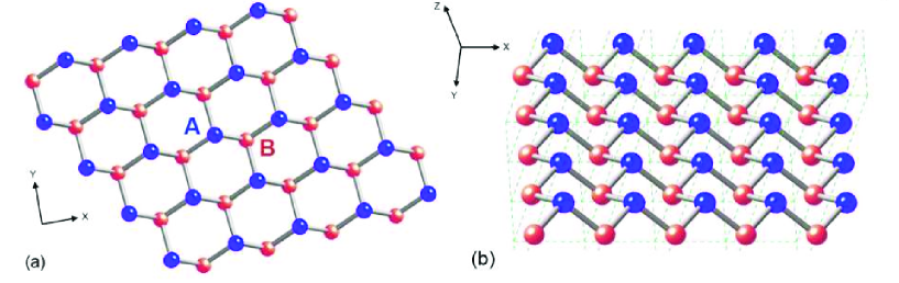
Graphene is the thinnest material in the world - a single layer of carbon atoms with a hexagonal structure Novoselov1 (cf. Figure 1a). It is one of the allotropes of carbon, diamond being another example, albeit with different physical properties. Graphene layers stack together to form a graphite crystal lattice, and can be found in the form of highly ordered pyrolytic graphite (HOPG) or even the core of a pencil Savage . There are four electrons present in the outer shell of a single carbon atom. For graphene, there are three bonds and one bond present. The bonds are an orbital hybridisation - a mixture of orbitals , thus providing a strong binding force for its atomic neighbours. The remaining electron orbital constitutes the bond. These are responsible for the half-filled band that enables free-moving electrons, thus displaying a metallic characteristic Wallace . Graphene is also capable of being combined with hydrogen or oxygen to form ‘graphane’, or other carbonic compounds respectively.
At low temperature, suspended graphene may also give rise to small quantum corrugations, whereby the two sub-lattices (A and B) are shifted with respect to each other in a transverse direction (cf. Figure 1b). The distance is of the order equivalent to some fraction of the inter-atomic spacing. At room temperature, the shape is nearly flat, with corrugation remaining only on the large scale Meyer . Here, low temperature microscopic quantum corrugations are transformed into transverse thermal vibrations.
In 1947, Wallace Wallace first studied the electronic band structure of monolayer graphite (graphene) by applying the simplest tight-binding model with a single hopping integral. He showed that the conduction band is half-filled, with an electronic spectrum that is gapless at six points of the Brillouin Zone. In vicinity of these points, the energy-momentum spectrum has a conical, Dirac form. These six points are therefore referred to as the Dirac points. He concluded that within two-dimensional graphene, an electrical conductivity should theoretically exist. A year later, Ruess and Vogt Geim2 ; Dreyer ; Ruess observed thin-film graphene oxide (GO) pieces using transmission electron microscopy (TEM). A single layer of graphene oxide was then discovered by Boehm et al. Geim2 ; Boehm1 ; Boehm2 in the early 1960s, and it was Boehm et al. who first proposed the name ‘graphene’ in their studies Boehm1 ; Boehm2 . Nevertheless, all these systems were found to be insulating. Although research on graphene, graphene-like structures and epitaxial graphene films continued for decades (cf. for example Gall ; Berger ; Sadowski ), it has significantly intensified since 2004, when Geim and his fellow researchers Novoselov1 successfully segregated graphene flakes from graphite using the simple scotch-tape method Geim1 ; Novoselov4 . This process will be elaborated upon in Section II.A. They subsequently went on to show that a graphene layer, separated from graphite, is an example of a two-dimensional structure possessing outstanding electrical properties Novoselov1 ; Novoselov4 . It is therefore no surprise that a huge number of studies on the physical and chemical properties of graphene have emerged in recent decades.
Recently, there has been strong progress in development of many graphene applications. Graphene’s unique electrical properties make it an ideal material for many electronic devices – in particular, graphene based transistors. In the present article, we describe various designs of graphene transistor that have been recently proposed, and how they capitalise upon graphene’s high electron mobility and conductivity.
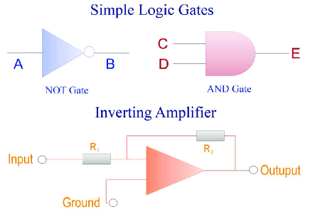
The field-effect transistor (FET) was first reported by J. Barden and W. H. Brattain in the 1940s at Bell Laboratories Bardeen . A transistor is the basic building block of many electronic circuits, normally acting as a logic gate or inverting amplifier in integrated circuits (cf. Figure 2). According to Moore’s law, the size of a circuit decreases roughly by half, every 1.5 years Schwierz . However, the scaling techniques, as well as the speed of the devices, have both reached a bottleneck in recent years. This is mainly because the decreasing scale leads to an increase of the energy dissipation per unit area (i.e., power density). The operating speed is also limited by the mobility and thermal conductivity of existing materials. New materials are thus highly sought after, to alleviate such aforementioned drawbacks. This article gives a brief review of the most up-to-date properties of graphene, electronic devices and transistors, together with their operational mechanism.
II Existing Fabrication Methodologies
The type of graphene (characterised by different properties) depends strongly upon its method of preparation. Three methods in particular, include mechanical exfoliation from bulk graphite Novoselov4 , graphitisation of silicon carbide (SiC) substrates (epitaxial growth) Heer ; Emtsev , and chemical vapor deposition (CVD) on various transition metals Chen2 ; Kim ; Li . In terms of the quality of graphene (such as mobility or structural defects), the exfoliated graphene produces the best material, followed by epitaxial graphene, and finally, CVD methods.
II.1 Mechanical Cleavage
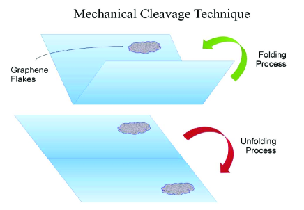
Mechanical cleavage is one of the simplest methods of fabricating a graphene layer Geim1 ; Geim2 ; Geim3 ; Katsnelson ; Novoselov4 . The process is similar to a folding and unfolding technique (as shown in Figure 3). One has to first cut the surface of a graphite sample Geim1 ; Geim2 ; Geim3 , usually with highly ordered pyrolytic graphite (HOPG) being used Iyechika . A small piece of graphite is then placed upon the sticky surface of adhesive tape Iyechika . The tape is folded and unfolded, with gradually more and more layers being stripped away Geim2 . The graphite is therefore made thinner - the procedure being repeated until what remains is one, or few layers of graphene. Monolayer graphene can be verified through a simple optical microscope via light interference patterns Novoselov4 , or also via Raman spectroscopy Geim3 . The mobility of exfoliated graphene can reach 15,000 cm2V-1s-1 Schwierz . Despite being a relatively simple way to produce graphene, this method produces only small quantities each time Novoselov4 .
II.2 Vacuum Epitaxial Growth Technique
An alternative means of fabricating graphene is via the epitaxial growth technique. Graphene produced in this way would usually possess an intermediate range of values for the mobility, smaller than for exfoliated graphene, but larger than for CVD graphene. Silicon carbide (SiC) is coated on a silicon wafer, with high temperatures being required Geim1 ; Geim3 ; Iyechika . Both silicon and carbon atoms would then individually become segregated. As the silicon atoms are evaporated by temperatures in excess of , only carbon atoms remain Geim1 ; Geim3 ; Iyechika and graphene will subsequently grow on the substrate Iyechika . Regardless, structural defects are always found since carbon atoms will sometimes be burnt due to the high temperatures - thus being contaminated by oxygen and hydrogen Iyechika .
The quality of epitaxial graphene can be conveniently analysed with the use of Raman spectroscopy. In particular, studies of the Raman active, single phonon (G band) and the two-phonon (2D band) are popular Hlawacek ; Robinson ; Trabelsi . Analysis of the position and shape of these Raman scattering lines provide much useful information. For example, the observation of a high-frequency shift of the G peak may describe graphene doping and associated changes in electron mobility Das . It is also highly beneficial for the monitoring of dopants (via Raman scattering) in an electrochemically top-gated graphene transistor. The local mapping of these Raman modes on the graphene surface (a method known as Raman topography) may describe the charge puddles created in graphene, as well as many other inhomogenous structures.
In particular, recent studies of the Raman topography of epitaxial graphene, show that the electron mobility is highly dependent upon thickness and monolayer strain uniformity Hlawacek ; Robinson ; Trabelsi . At room temperature, the highest mobility of epitaxial graphene (on the carbon-terminated face of the SiC substrate) reaches a value of 5,000 cm2V-1s-1 Schwierz . It was also shown that the carrier mobility depends strongly upon the stacking of graphene layers Hlawacek . It is worth mentioning that for exfoliated graphene (produced by mechanical cleavage method (cf. section II.A)), the mobility is higher when compared to that via the epitaxial growth technique Novoselov1 ; Schwierz .
II.3 Chemical Vapor Deposition
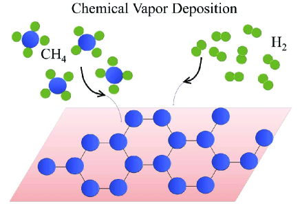
Chemical vapor deposition (CVD) is usually used in industry Iyechika , since it can be easily mass produced. The process involves high-temperature chemical reactions with hydrocarbon gases (e.g. and ) and a catalytic metal surface such as either copper or nickel (cf. Figure 4). These metals help decompose the chemical bonding Geim1 ; Geim3 ; Iyechika , and order carbon atoms into a hexagonal (honeycomb) lattice. Hence, the larger the metal surface, the larger the quantity of graphene that can be produced. For this purpose, the most popular is a polished polycrystalline copper foil. It is easy to transfer graphene from this metal surface to other substrates – for example, by applying a voltage. Therefore, the CVD method exhibits large scale superiority with respect to other graphene production methods. It is a relatively simple and low-cost method which allows the growing of monolayer graphene to large size Bae . However, the charge carrier mobility of CVD graphene is generally lower than data reported for exfoliated graphene Bae ; Du ; Chen3 ; Bolotin ; Morozov ; Kusmartsev . It was found that the main source of this low mobility is the presence of grain boundaries Song . This has been well studied with the use of both transmission electron microscopy (TEM) and scanning electron microscopy (SEM). The point defects, as well as surface contamination, are further key factors which significantly affect the mobility. The mobility of a short channel device, where the grain boundary is absent, can reach 2,700 cm2V-1s-1. In the presence of this boundary, it will be roughly three or four times smaller Song ; Hlawacek .
III Physical Properties of Graphene
III.1 Graphene Electrical Conductivity
Mobility is a measure of how fast the carriers propagate in an electric field. Its value depends upon the type of material and the interaction with substrates. After the process of annealing, some suggest the mobility of exfoliated graphene can reach values upwards of 200,000 cm2V-1s-1 Neto ; Schwierz ; Kusmartsev in a perfect structure. Recently, experiments with graphene Sarma show that at this specific point, there should be a minimum conductivity in graphene Geim3 . This is around double the value for the conductance quantum , observed in quantum wires Yang-Bo . This value is independent of the material properties and length of the quantum wire Datta . It is also of particular interest that the concentration of electrical carriers at the Dirac point tends to zero. Here, even at room temperature, the charge-carriers may perform long range (ballistic) transport without much scattering at all Geim3 ; Du ; Kusmartsev . Graphene is also useful for electronics, especially due to its elasticity and strong resistance against destruction. Young’s modulus for graphene can be as large as 1TPa Neto . Graphene is the strongest material in the world, around 100 times stronger than steel Savage . Yet, due to its monolayer structure (cf. Figure 1), it can be stretched and bent rather easily.
III.2 Thermal Conductivity
Using high-resolution vacuum scanning thermal microscopy, it was found by Pumarol et al. Pumarol that thermal conductivity in suspended graphene is carried by ballistic phonons. Hence, the thermal conductance of graphene on a substrate will significantly downgrade, since the number of scattering channels increases. In this case, heat may be lost to the substrate. The thermal conductance also decreases with an increased number of graphene layers. Analysing nano-thermal images, it was found that the mean-free-path of thermal phonons in graphene on a substrate, is smaller than 100nm. According to Prasher Prasher , the thermal conductivity of graphene on a silicon-dioxide substrate can reach around 600 Wm-1K-1, incidentally higher than copper. Other papers provide even higher values for the in-plane thermal conductivity, but of the same order of 1,000 Wm-1K-1 Balandin ; Seol . The heat flow between graphene and the substrate, would influence the dissipation, due to the high in-plane thermal conductivity Koh . Thus, in-plane heat transport for graphene is associated with acoustic phonons Pumarol ; Seol . However, the mechanism of heat transport across graphene interfaces in the cross-plane direction is currently unknown, as mentioned by Koh et al. Koh
III.3 Photonic properties
Single layer graphene absorbs a mere of visible light (where is the fine structure constant Nair ), thus possessing a high transparency Rafiee . Graphene provides a wide range of absorption across the visible light spectrum. Bonaccorso et al. Bonaccorso mention that the peak of absorption is in the ultraviolet domain, because of the van Hove singularity. The peak arises due to the van Hove singularity in the energy density of states (DoS). It is, in fact, a well suited material for photonic devices. Being almost perfectly transparent to visible light due to its atomic thickness, such a material can be made available for small screen devices Rafiee ; Savage ; Prasher . For similar reasons, there is also common belief that graphene’s true potential lies in opto-electronics, as discussed by Nair et al. Nair and Bonaccorso et al. Bonaccorso .
Stoehr et al. Stoehr observed white optical luminescence of graphene, when subject to picosecond infrared laser pulses - this creates a high density electron-hole plasma. The luminescence arises due to electron-hole recombination, created in a broad energy range. There are two relaxation mechanisms observed in the graphene electron-hole plasma Breusing . The first relaxation mechanism relates to the intra-band electrons and holes collisions, with a duration of around hundred femtosecond. The second one arises from the cooling of hot optical phonons, with around a few picoseconds, which is slower than first mechanism O'Hare ; Bonaccorso ; Kampfrath ; Lazzeri ; O'Hare2 .
III.4 Energy Spectrum and Anomalous Quantum Hall Effect
Graphene has a closely packed, periodic structure of carbon atoms, and consists of two carbon sub-lattices (A and B) per unit cell Savage (cf. Figure 1a). As previously mentioned, there are six Dirac points in the corners of Brillouin zone, with a linear, conical relationship being found in the lower part of the energy-momentum spectrum. This can be approximated by the following dispersion relation Wallace ,
| (1) |
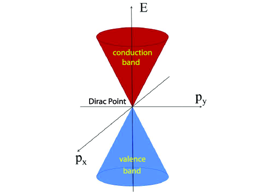
where is Fermi velocity, and and are the electron momenta in the graphene plane. The points in momentum space where the energy vanishes (i.e., ) are called the Dirac points. A single Dirac cone for the graphene energy spectrum is shown in Figure 5. At the Dirac point, there is a direct contact of the conduction and valence bands Novoselov1 ; Novoselov2 ; Katsnelson , possessing a zero energy band-gap Geim3 ; Iyechika ; Wallace . Graphene also exhibits zero effective mass, and is well described by the relativistic Dirac Hamiltonian and equation:
| (2) |
where , and . Electron momentum is given by Geim3 . Wave functions and relate to sub-lattices A and B respectively, and refers to the vector of Pauli matrices :
| (3) |
The eigenvalues of this 22 Hamiltonian , immediately give the Dirac spectrum (cf. equation (1)). Furthermore, charge-carriers in graphene travel at 1/300 the speed of light Geim3 ; Fal'ko ; Katsnelson (), thus providing a miniaturised platform to test the phenomena of quantum electrodynamics (QED) Geim3 without the use of expensive accelerators. In general, quantum behavior is normally exhibited at low temperature; such processes include the QHE, where the transverse Hall resistance is quantised. However, with graphene, the possibility has now arisen to study such quantum behavior at room temperature Novoselov3 ; Katsnelson . Some of the most recent experimental research Novoselov2 ; Novoselov3 ; Dean has reported observation of the QHE within a graphene monolayer, displaying quantum resistance at room temperature. Integer QHE in graphene is slightly different to that of standard two-dimensional semiconducting devices. Here, the quantised conductivity has an additional shift equal to one half of the minimum conductivity . The fractional QHE in graphene is associated with the electron-electron interaction as in other semiconductors, and a four-fold degenerate state originating due to the existence of the two degenerate sub-lattices (A and B) Geim3 ; Novoselov2 ; Novoselov3 ; Dean ; Jiang . Both fractional and anomalous QHE have been observed within the single monolayer, as well as bilayer graphene Novoselov3 ; Katsnelson ; Dean .
III.5 Quantum Klein Tunneling
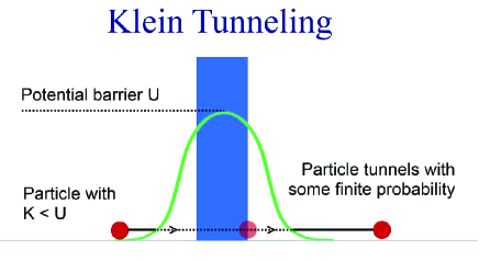
Graphene provides a new quantum feature with regards to tunneling Katsnelson2 ; Calogeracos1 ; Su ; Calogeracos2 . In classical mechanics, an electron with kinetic energy cannot penetrate a potential barrier when . Interestingly, quantum theory shows that there is a certain probability of transmission, even when . Furthermore, under certain conditions, relativistic quantum mechanics permits an electron to tunnel in a straightforward manner through the barrier with perfect transmission Calogeracos1 - a process called Klein tunneling. Katsnelson et al. Katsnelson2 reveal that Klein tunneling can occur in graphene, as depicted in Figure 6. It is further surprising that a perfect transmission occurs in graphene Katsnelson2 . Overall, it appears as if electrons penetrate the square potential wall, without restriction being placed upon on its height. In reality, it is very difficult to manifest a perfectly square potential – graphene will always have a smooth potential.
Recently, Zalipaev et al. Zalipaev discovered that certain shapes of potential well (e.g., parabolic) would influence the tunneling behaviour of an electron in graphene (cf. for details Zalipaev ). There is a drastic difference between tunneling through smooth and rectangular barriers. The Klein tunneling features are clearly exhibited only for a rectangular barrier. The type of the tunneling behavior depends upon the energy of the particle relative to the barrier height, and the angle at which the particle is incident to the potential barrier. When the energy of the particle is close to the top of the barrier, one observes conventional tunneling. For intermediate energies, the smooth potential acts as a Fabry-Perot interferometer. However, for energies close to the Dirac point, confined bound states will arise Zalipaev . The confinement effect at small energies for the special waveguide geometry, can also be found in references Hartmann ; Wu ; Williams . The conducting waveguide channel in electronic devices is usually created by a gate voltage applied to graphene. This leads to the lateral confinement of electrons within the channel. However, electrostatic potentials of the circular form which are very smooth (i.e., do not have exponentially decaying tails), may possess a threshold for the appearance of the zero-energy confined state Downing ; Stone . This may lead to an unusual Aharonov-Bohm (AB) effect in graphene (e.g., the fractional AB effect arising in strongly correlated electrons) Kusmartsev-1995 .
III.6 Quantum Capacitance
Quantum capacitance is one of the most interesting properties of the graphene capacitor, as reported by Yu et al. Yu . Total capactiance in graphene is given by , where is related to classical electrostatics, and is the quantum capacitance. is proportional to (where is the electron density and is the chemical potential), and also the number of electron states (spin up/down) near the K and K’ points of the Brillouin zone Yu . The density of states (DoS) in two-dimensional graphene associated with energy is given by Katsnelson
| (4) |
where Planck’s constant Js, with a Fermi velocity for graphene. At zero temperature, the Fermi energy coincides with the chemical potential . The quantum capacitance can then be described by the analytic expression
| (5) |
where is the surface area of the capacitor electrodes Yu and the electron density is related to via the equation:
| (6) |
The degeneracy factor takes into account the double spins, and valley degeneracy of the Dirac spectrum for graphene (i.e. ). For zero applied electric field (i.e., zero gate voltage), both the chemical potential and DoS are very small. At low temperatures, the chemical potential then takes a very simple form:
| (7) |
For example, consider an epitaxial graphene layer doped to an electron density cm-2. The chemical potential is then shifted above the Dirac point due to the doping. We can immediately estimate both the chemical potential and the Fermi energy, = 0.1167 eV. Then, the quantum capacitance per unit area is equal to . For pure graphene subject to a small applied voltage, is very small, and hence the dominant contribution to the total capacitance Kusmartsev . This is the so-called graphene quantum capacitance effect (cf. for details Xia et al. Xia and Giannazzo et al. Giannazzo ). However, as an applied electric field is increased, more electrons occupy the conduction band, and shifts to an upper value. becomes larger compared to , with the quantum capacitance effect becoming less important. Recent studies have discovered that can reduce significantly due to disorder of the graphene structure, as mentioned by Li et al. WLi . In general, the contribution is much smaller than in the presence of an electric field. Therefore, the capacitance of graphene simply reduces to the electrostatic case ().
IV Graphene Materials
It is important to have a brief introduction of the electronic properties of carbon nanotubes (CNTs) Avouris ; Tans ; Zhu ; Martel ; McCann and graphene nanoribbons (GNRs) Li2 before discussing graphene devices Park ; He ; He2 . Fal’ko and McCann first showed that both GNRs and single-wall CNTs are described by the Dirac Hamiltonian of equation (2), with various periodic and hard-wall boundary conditions McCann . The application of CNTs, designed to act as the channel of a graphene transistor, will be further discussed in section VI.
IV.1 Carbon Nanotube
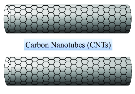
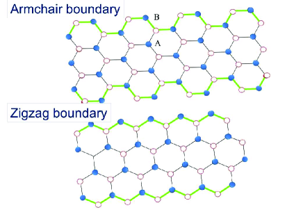
A carbon nanotube (CNT) can be formed by rolling or twisting a graphene ribbon into a cylindrical configuration Avouris . CNTs are often referred to as a one-dimensional nanostructures, due to their tiny radius Avouris (cf. Figure 7). These CNTs can be either single-walled or multi-walled, dependent upon how many monolayers exist Martel (for details concerning the synthesis of CNTs, one can refer to Zhu ). Nevertheless, this folding of graphene leads to deformation of the carbon atoms, thus altering its electronic band properties Avouris ; Tans ; Martel . In general, the band structure of CNTs is determined by the boundary conditions (BCs), specified by the folding angle and radius of the CNT (sometimes known as the chiral index) Avouris ; McCann . This, in turn, determines whether the CNT is a conductor or a semiconductor. Generally, the boundary of a CNT can be classified as having zigzag or armchair structure, or a mixture of both (cf. Figure 8 for the GNR). Zigzag CNTs are conductors, whereas armchair CNTs can either be a conductor or semiconductor (dependent upon the radius of the nanotube) Avouris ; Tans ; Martel . This radius is found to be inversely proportional to energy band-gap
| (8) |
The wave function of the CNT is also subject to a periodic boundary condition, thus determining the degeneracy of energy states Iyechika ; Avouris ; Tans ; Martel . The nanotube can also act as a good transistor channel between the source and drain, since the carriers exhibit long range (ballistic) transport at room temperature Avouris ; Tans ; Martel . Transistor operation and contact effects will be further elaborated upon in section VI.D.
Single-walled CNTs are a single layer of graphene curled into a hollow cylinder. Recent research by Martel et al. Martel , states that the drain current decreases as the applied gate voltage is increased above the CNT channel. They report that carriers in CNTs come from holes (p-channel) which may either be created due to deformation, or the contacts between the CNT and electrodes Martel . For zero gate voltage (), a current will flow through the channel. Conversely, for a large positive gate voltage (), no current is observed Martel .
Multi-walled CNTs, on the other hand, constitute a roll of multiple layers of graphene. Martel et al. Martel report that no field effect was found, and that multi-walled CNTs are conductive. It is because the radius of a multi-walled CNTs is larger than those of single-walled, that the band-gap is very small Martel .
IV.2 Graphene Nanoribbon
A graphene nanoribbon (GNR) is a graphene sheet possessing a very small width Iyechika ; Avouris . A GNR can be obtained by cutting a CNT along its axis, with a scale ranging from 10-100nm Avouris ; Li2 . As with the CNT, the BCs of a GNR determine whether system behaves as a conductor or semiconductor. The zigzag BC corresponds to a conducting GNR, whereas the armchair BC can either yield a conducting or a semiconducting characteristics Iyechika ; Avouris ; Li2 . Electrons can become trapped in a small confined region of the GNR with a certain BC, thus forming an energy band-gap Li2 . For the armchair structure, this band-gap should be (in theory) inversely proportional to the width of the nanoribbon Iyechika
| (9) |
Current experiments, however, have shown that the band-gap observed does not rely upon the width and chiral index Iyechika ; Avouris ; Tans ; Martel ; Li2 . It may be plausible that the lithography and etching techniques are inadequate to define the orientation precisely Avouris ; Li2 . Therefore, hybrid structures (combinations of armchair and zigzag GNRs) always co-exist within a sample. In any case, phonon scattering near the edge of the nanoribbon would also downgrade the mobility Avouris .
V Applications of Graphene Devices
Some common applications of graphene to electronic devices are discussed below. These include graphene sensors He ; He2 , photonic and optical devices Iyechika ; Engel and capacitors. Details of graphene transistors will be discussed in section VI.
V.1 Graphene Sensor
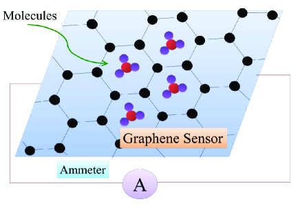
Impermeability is one of the most outstanding properties of graphene, since the carbon atoms are closely packed with one another Savage . Furthermore, the conductivity of graphene is sensitive to impurities, and can change easily when other molecules or substrates become attached to it. The variation of such conductivity due to molecular attachment is the principal foundation for molecular sensors (cf. Figure 9) He2 . Graphene, with its two-dimensional surface, provides a platform upon which tiny particles can attach. The deviation of electrical resistivity, caused by the attached molecules (impurities), can be measured by the Hall Effect He ; He2 . He et al. He ; He2 have successfully developed bio-sensors and gas sensors using such a method. In the near future, graphene is also likely to be a plausible candidate for magnetoresistance sensors Tom .
V.2 Graphene Photonic Devices
There is no doubt that graphene film is an ideal material for photonic devices Rafiee . Due to the fact that graphene’s atomic thickness has little absorption of light, this makes it almost transparent to all visible wavelengths O'Hare ; Avouris (cf. section III.C). As such, there are a number of applications, including solar photonic devices, touch screens and graphene photonic transistors Engel .
Optical semiconducting devices are derived from the working principle of the photo-electric effect. Photons transfer their energy to electrons, which can only absorb photons of specific wavelength. Donors are generally doped so as to increase the Fermi level. The absorption range will therefore be reduced, thus enhancing the sensitivity to photon absorption or emission Engel ; Rudden . Under the influence of an electric field, the emission of photons (due to recombination of the carriers) is referred to as electro-luminescence Avouris . Note that some recombination may also relate to the process of thermionic emission. Additionally, photo-conductivity is the process of photon absorption, whereby the conductivity is increased due to the excitation of additional carriers. This process leads to the creation of additional electrons and holes in the conduction and valence bands Avouris ; Rudden . As such, one could potentially apply this premise to that of light detectors. Indeed, Kim et al. Kim2 further noticed that a graphene light detector can have a transit bandwidth reaching speeds of up to THz.
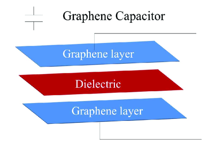
V.3 Bilayer Graphene Capacitor
The working principle of the graphene bilayer capacitor is to store charge and bypass high-frequency signals Miller . A simple graphene capacitor consists of two graphene layers, separated by a dielectric medium (cf. Figure 10 for a schematic representation). Graphene is ideal for storing charge due to its high mobility. Furthermore, a single atomic layer is also capable of minimising the overall size of the capacitor Miller . Interestingly, a graphene capacitor has ambipolar characteristics within the electrodes (the electrodes being either positive or negative), thus simplifying the manufacturing process Miller . Miller et al. Miller have also reported that the response time for a capacitor should be fast enough to react to high-frequency circuits. Therefore, the time constant () is made as small as possible, where is the internal resistance and is capacitance. It is important to also note that is inversely proportional to cutoff frequency . If one requires large capacitance for charge storage, the internal resistance inside the capacitor is required to be very small. Graphene, with its low resistance, is therefore an ideal material for the next generation of capacitors. Miller et al. Miller further go on to show that graphene bilayer capacitors can perform extremely well at high frequencies. Thus, the aforementioned graphene devices may be very useful for ‘green’ energy storage.
VI Developments and Hurdles of Graphene Transistors
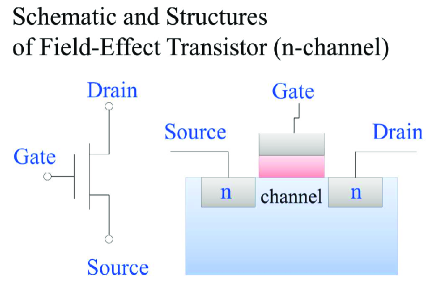
We have already highlighted upon some of the major applications of graphene devices in previous section. However, they have also created a firm base for the next generation of the graphene electronics – graphene transistors. Transistors (which are made of semiconductors) are a key constituent of many electronic devices. These include inverting amplifiers, or logical controllers in integrated circuits. Generally speaking, a field-effect transistor (FET) consists of three terminals - gate, source and drain (cf. Figure 11). An electric current flows between the source and drain via a channel, and the current flow rate can be controlled via the gate voltage Irwin . The gate oxide layer is a dielectric between the gate and channel. Impurities are also introduced via doping, to increase the concentration of charge-carriers on the channel Rudden ; Irwin ; Turton . Two types of carriers: p-type (acceptor) and n-type (donor) are commonly used in industry. The materials constituting an FET (source-channel-drain) are typically of either n-p-n type or p-n-p type Rudden ; Irwin ; Turton . The scale and speed of silicon-based transistors has undergone leaps in performance over recent decades. Nevertheless, the limit of transistor size has reached an optimal level, with new materials urgently being required to replace silicon. Graphene, a revolutionary new material, looks set to fill this void due to its outstanding electronic properties Wallace ; Avouris .
VI.1 Band-gap of Graphene
VI.1.1 Insulator, Semiconductor and Conductor
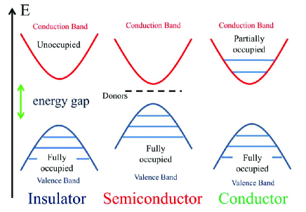
The electrical conductivity of a material can be split into three categories: insulators, semiconductors or conductors, according to its band structure (cf. Figure 12). Electrons are not able to move freely within an insulator, as the valence band (fully occupied by electron states) and conduction band (unoccupied) are separated by an energy band-gap . The semiconductor, however, is the basic building block for an ON/OFF switching device, as it possesses only a small energy band-gap Rudden ; Irwin ; Turton . For example, silicon is a commonly used material within semiconductors, and is generally doped (via some donor for example) in order to make an electron excite more easily to the conduction band. In semiconductors, electrons can also be activated into the conduction band via the increase of temperature, or an applied electric field (up shift of Fermi level). Conductors normally relate to metals, as electrons are permitted to move freely in the conduction band. It is because metals have this partially filled conduction band, that electron excitation is gapless.
VI.1.2 Methods of Band-gap Creation in Graphene
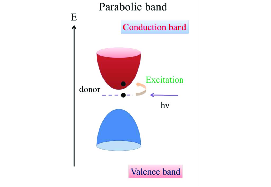
Figure 13 shows that the electronic band structure of a semiconductor is parabolic, with a non-zero energy gap separating the conduction and valence bands Iyechika ; Schwierz . It is interesting to note that graphene has a linear cone band structure, and is gapless at the Dirac point, (cf. Figure 5 and section III.D) Novoselov1 ; Geim3 . Small thermal fluctuations, or the application of an electric field may excite electrons from the valence to conduction band within graphene Novoselov1 . The Fermi energy will rise in the presence of an applied electric field (dependent upon the sign of the applied gate voltage), and thus exhibit a metallic characteristic. Additionally, there exists an electrical potential of the graphene sheet relative to some carrier reservoir – this is determined by the geometry of the device. The zero band-gap of graphene is clearly an obstacle with regards to its application in semiconducting devices, as no precise OFF state is provided Avouris ; Kim2 . Accordingly, opening the band-gap is the most important task in making the graphene transistor become a practical reality.
Several existing methods to create the gap include carbon nanotubes, graphene nanoribbons, deformed structures and bilayer graphene, to act as a transistor channel Geim3 ; Schwierz ; Avouris ; Kim (cf. section IV). Graphene oxide is also capable of providing a small energy band-gap due to the change of electronic band structure Iyechika ; He ; He2 . Another possibility is via deformation of the graphene layer, either by bending or physical strain, since theoretically, the band-gap properties depend upon the width and orientation of the graphene allotrope Geim3 ; Iyechika ; Li2 . A small band-gap in graphene can also be created via chemical doping, or by retaining some of the defects in the structure as mentioned by Coletti et al. Coletti and Terrones et al. Terrones . As previously discussed, doping in a silicon semiconductor is achieved by replacing some atoms of silicon with other elements. However, this is slightly different for the case of graphene. Due to the strong honeycomb structure, the dopants are generally placed upon the graphene surface, rather than by replacing a carbon atom itself. This leads to a structural defect, and thus changes the electronic band structure. This means that the band-gap can therefore be controlled. Some common dopants include gold, sulphur, boron and nitrogen Coletti ; Terrones . Boron nitride (BN) is one of the key compounds for the doping of graphene, and subsequent band-gap creation Fan ; Shinde . Fan et al. Fan have also discovered that BN, doped in a ‘random’ pattern upon the graphene surface, is capable of opening a band-gap. They report that the distribution of surface charges (electrons in bond configuration) is altered by doping, hence forming a small band-gap. However, existing doping methods are sometimes not simple to control KYan . However, Yan et al. KYan have recently reported that doping via CVD methods can offer a more simple and stable means of creating this band-gap.
As discussed in section IV.A, the CNT is a traditional method of opening the band-gap, and is dependent upon the choice of boundary conditions (characterised by the chiral index) Avouris ; Tans ; Martel . Bilayer graphene has a zero band-gap, although an applied electric field can be implemented to create such a gap Iyechika ; Schwierz (details of the band-gap in bilayer graphene can be referred to in Kruczynski ; Gradinar ). Deformation of graphene structures has also been known to control the band-gapIyechika . Nevertheless, in all cases, developing a band-gap within graphene would normally reduce its mobility Iyechika ; Schwierz .
Schwierz Schwierz has stated that the mobility of GNRs only falls within the range of cm2V-1s-1 Schwierz . The decrease is due to dislocations present in the graphene crystalline structure, most likely induced during the manufacturing process. It is widely known that the speed of the carriers is proportional to their mobility - thus the tradeoff in creating a band-gap is to slow down the speed of the device Rudden ; Turton . As mentioned by Schwierz Schwierz , an ON/OFF switching state is not well-defined in current technologies, and much effort has been focussed upon this area. Alternatively, graphene may be suitable for high-frequency devices, which do not require a well-defined OFF state.
VI.1.3 Band-gap on Substrate in Electric Field
As previously mentioned, the most general shape of suspended graphene consists of two sub-lattices (A and B), which can be displaced with respect to each other in a transverse direction O'Hare (cf. Figure 1b). If graphene is coated on a substrate, this will give rise to some force (including the van der Waals) upon the interface. The sub-lattices should differ with up and down transverse displacements along with the z-axis, assuming that an electric field is applied. This means that symmetry between the up and down (out-of-plane) displacements is broken. For a single valley, we may estimate the value for the band-gap directly via the 22 Dirac Hamiltonian matrix:
| (10) |
where describes a stress induced by the substrate, is the electric field in z direction, and is one of the Pauli matrices. The eigenvalues of this matrix specify the Dirac spectrum , with a value for the band-gap equal to O'Hare .
The application of a transverse electrical field (of amplitude ) can also induce polarisation of sublattices (A and B). This is described by the same invariant term in the Hamiltonian as . We have , and thus a band-gap equal to O'Hare . To have visible band-gap, the value of is required to be large. The best way to realise this mechanism, is to use a ferroelectric material for the substrate. However, the deformation phenomena are of utmost importance here O'Hare . Due to the transverse lattice displacements separating the sub-lattices (A and B), there arises a deformational field with a value of the order . Here, is the deformation potential, ‘’ is the inter-atomic spacing, and is the change of transverse displacement which arises due to the presence of the substrate. In the following estimation for the energy band-gap, we use the following parameters for graphene, and the deformation potential is equal to eV Kaasbjerg . If we assume that is around 10% of the transverse displacement , which is roughly equal to (the order of magnitude estimated for silicene Drummond ), this gives an energy band-gap meV O'Hare ; Drummond . Thus, in the addition to deformation from the substrate, the application of can contribute an additional force to the substrate, and may provide a further means of controling the band-gap. This value can increase or decrease linearly with the applied electric field. The phenomenon is general, and also arises in other two-dimensional crystals (cf. for example, silicene O'Hare ; Drummond ).
VI.2 Electric Field Effect in Graphene
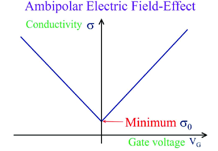
Geim et al. Novoselov1 have observed that electric field effects were found in two-dimensional graphene, and that such effects were stable at room temperature. Figure 14 shows the schematic behavior of electrical conductivity in the presence of a gate voltage . A minimum conductivity is also shown to exist at the Dirac point. Although there exists a zero charge density at this point, nevertheless, it exhibits metallic properties Novoselov1 . A linear relationship between conductivity and gate voltage is found for an uncontaminated graphene film, with positive and negative slopes when and respectively Geim3 ; Novoselov2 . This indicates that conductivity is proportional to the DoS at the Fermi energy. An ambipolar characteristic within the electric field has also been discovered, and that either holes () or electrons () could both act as transport carriers Fal'ko .
In the early studies of Geim et al. Novoselov1 , hole carriers were found to exist even at . Here, water vapor molecules attach to the surface of the film, thus changing the polarity. These water molecules can, however, be removed via the process of annealing Novoselov2 . Recent reports Geim1 ; Geim2 ; Neto also reveal that the mobility is stable when subject to a change of temperature. Only structural defects can affect the mobility of a sample - this would not reduce significantly, even in the presence of high electric fields. A monolayer graphene channel would also appear to remedy the short-channel effect present in silicon-based transistors. Such an improvement is one of the key foundations for a faster logical transistor.
Schwierz Schwierz also points out that a graphene transistor might have some special characteristics, possessing two linear regions and one saturation region. When the drain-source voltage is small, a linear relationship for the curve is found. As is increased further, a saturation of the curve begins to emerge. If exceeds a certain limit, a new linear region is yet again observed. Only a few studies with current saturation have been reported. A greater understanding of characteristics would require addressing in the near future, as this saturation region would affect the performance of devices.
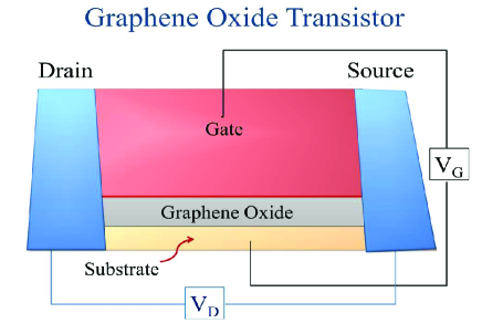
VI.3 Graphene Oxide Transistor
A number of conventional graphene transistors, of various design, have been proposed in recent years. In principle, graphene can easily act as a transistor channel Avouris . Graphene oxide (GO) is a compound of both graphene and oxygen Geim2 ; Iyechika , a single layer of which is slightly thicker than a graphene monolayer Jin . Jin et al. Jin claim that the use of graphene oxide is one of the simplest ways to create an energy band-gap, thus turning graphene into a semiconductor. Graphene oxide is water soluble, and the fabrication process is not at all complicated. Recent studies Jin have reported that graphene oxide can be tuned to either a semiconducting or insulating state, dependent upon the amount of oxygen, and bonding structure therein. A thin graphene oxide layer is generally coated on a silicon substrate, acting as a channel for the transistor. A schematic of a graphene oxide transistor is shown in Figure 15, and exhibits an ambipolar characteristic for a clean sample Jin . It was also discovered that the drain-source current increases with the absolute value of gate voltage Jin . The drain-source current was also found to be increasing with temperature. Despite the mobility of graphene oxide being much less than for graphene (cm2V-1s-1), the main advantage of this method is its simplicity, requiring no reduction process (cf. Jin et al. Jin ).
Reduced graphene oxide (rGO) is obtained via a chemical process of removing oxygen from graphene oxide Iyechika . However, reduction is not always perfect. Defects in the honeycomb structure are usually found in experiments Iyechika ; Dreyer ; Jin , with residual oxygen compounds sometimes remaining on the boundary of samples He ; He2 ; Jin . High temperatures can remove the oxide components, but are required to be in excess of 1000K. Like graphene oxide, reduced graphene oxide can act as the channel inside an FET He2 . He et al. He2 have applied a coating of reduced graphene oxide to polymer substrates (3-aminopropyltriethoxysilane PET substrate), discovering an ON/OFF switching ratio of approximately 3-4. This switching ratio is determined by how the current responds to the gate voltage - from the OFF to ON state, or vice versa. They further reveal that the conductivity of a transistor depends upon the thickness of the rGO electrodes - the mobility also degrading as a result of structural defects. However, even in the absence of a gate voltage, a non-zero drain-source current still exists, and thus current leakage may occur. He et al. He2 also mention that a bending of reduced graphene oxide would widen the transition region of the ON/OFF state, thus reducing the switching ratio.
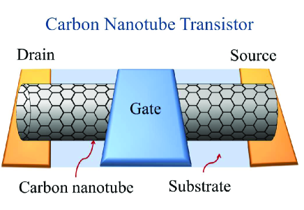
VI.4 Carbon Nanotube Transistor
A number of theories and experiments with CNT transistors Schwierz ; Avouris ; Tans ; Kreupl ; Franklin ; Jang have been undertaken for a few decades now, becoming a well-developed area of research. The CNT works as a transistor channel, capable of being tuned from conductor to semiconductor as mentioned by Tans et al. Tans . Figure 16 shows a diagrammatic representation of such a CNT transistor. In theory, the CNT channel can perform long-range (ballistic) electrical transport Schwierz . Avouris et al. Avouris have also proposed that the movement of electrons within the CNT structure is restricted to one dimension Avouris , thus limiting the amount of inelastic scattering. In brief, the performance of a CNT transistor can be characterised by its resistance , capacitance and inductance Avouris . In the studies of Avouris et al. Avouris , they further mention that these physical quantities (, and ) simultaneously exhibit both classical and quantum behavior - these quantum effects are found to be more important for a very small transistor size. In fact, the quantum resistance is of the scale , whilst quantum capacitance and inductance in CNTs are associated with the DoS (cf. for details Schwierz ; Avouris ). Capacitance and inductance, whether classical or quantum, depend upon the shape, size and boundary conditions of the CNT. Moreover, Schottky barriers are also found in CNT transistors, exhibiting a large resistance. These are due to the contact between the metal electrode and semiconducting CNT. Due to the differing work functions between the CNT and metal electrode, this leads to a consequent shift of the Fermi energy Avouris . Recently, it has been discovered that the shape of potential barrier, between the electrodes and CNT, is shallow and wide. They maintain quantum coherence of electron transport between the adjacent sections, for lengths even up to several micrometers Barbara .
Theoretically, ballistic transport is found throughout the CNT transistor, with a large mean-free-path of the carriers Schwierz ; Avouris . In the real case, like in metals and semiconductors, the electron transport is due to diffusion, thermal gradients and electric fields, together with the chiral index of CNT. The length of the CNT also determines the transport - the longer the nanotube, the more inelastic scattering that will occur Schwierz ; Avouris . The drain-source current can be controlled via an electric field acting upon the CNT channel. Two types of CNT transistor (top gate and wrap-around gate) were developed recently Schwierz ; Avouris . Avouris et al. Avouris have pointed out that the Schottky barriers in CNT-metal electrode contacts are very high when compared to those of silicon. Nonetheless, CNT transistors can work well upon inter-connection of intergated circuits, operating well even at room temperature Avouris . This is due to the small electron-phonon interaction inside the CNT. Overall, these transistors consume less power than their traditional silicon-based counterparts, thus proving to be an advantage for logic switches.
Franklin et al. Franklin have simulated a short CNT transistor (with 9nm channel width), with reports of better performance and stable electrical properties in comparison to silicon-based devices possessing a 10nm channel width. The study claims that the short CNT channel provides a faster switching speed. However, in a silicon-based transistor, a shorter channel would deteriorate its quality. The overall stability of the drain-source current is compromised when the channel is of the scale of tens of nanometers (i.e., similar to that of the depletion layer). The electrical current through the transistor thus becomes unreliable Avouris . This is more commonly known as the short-channel effect. According to Franklin et al. Franklin , the short-channel effect can be minimised by a thin CNT. In addition, Jang et al. Jang have also reported that CNTs provide a high switching ratio.
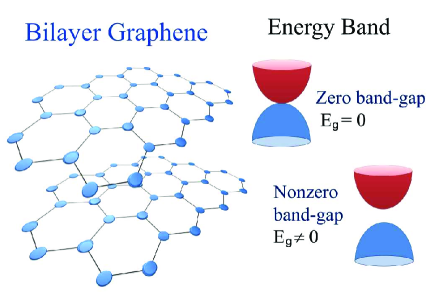
VI.5 Bilayer Graphene Transistor
Bilayer graphene consists of two individual graphene monolayers (cf. Figure 17). As expected, Sarma et al. Sarma have pointed out that the structure of bilayer graphene is similar to that of very thin graphite. Similar to monolayer graphene, the bilayer has a zero energy band-gap, but with a parabolic shape Iyechika . A perpendicular electric field applied to the graphene bilayer, or impurities via doping can, however, create a band-gap Iyechika . Furthermore, the magnitude of this electric field can tune the size of the gap Zhang3 . Ponomarenko et al. Ponomarenko have also reported that the bilayer channel can be changed from conductor to insulator by tuning the applied electric field. However, one cannot control the band-gap easily via doping Iyechika . The mobility in double layers is lower than that of a single layer, as stated by Wallace Wallace . Nonetheless, carriers in bilayer channels can still perform at high speed. Studies by Zhang et al. Zhang3 have discovered that the band-gap of bilayer graphene varies in the range of 0–298 meV at room temperature. This narrow gap is suitable for tunable nanophotonic applications, allowing a certain range of the visible spectrum to pass through Zhang3 . Another advantage of bilayer graphene, is that the current leakage can be minimal. A more concise understanding as to precisely how the band-gap of bilayer or multilayer graphene is affected by an external electric field, will urgently be required in the near future.
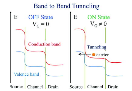
VI.6 Tunneling Graphene Transistor
Figure 18 shows the ON/OFF states of a transistor, with and without an applied gate voltage . As mentioned by Ionescu et al. Ionescu , the application of a gate voltage could control tunneling between the two bands. A tunneling graphene transistor possesses a steep sub-threshold slope, hence providing a fast response time Schwierz . The basic principle is that the applied gate voltage alters the shape (offset) of the conduction band, and hence the charge carriers from the conduction band could tunnel to the valence band. The choice of material for the channel inside is usually composed of either CNTs, GNRs or bilayer transistors Dean . Ionescu et al. Ionescu state that the current in tunneling transistors arises due to a leap of electrons between the conduction and valence bands, rather than via diffusive and thermal transport (the concept is similar to Landau-Zener tunneling Nandkishore ). In general, a tunneling transistor (via some quantum process) consumes much less power than a non-tunneling equivalent Ionescu . Michetti et al. Michetti have also proposed that within the tunneling graphene transistor, the ON/OFF switching ratio could reach as high as , and that tunneling could occur even with a small applied gate voltage. Overall, the band-to-band tunneling in a graphene transistor is generally dependent upon the band-gap width, channel length, oxide thickness and gate voltage Michetti .
Zhao et al. Zhao have studied a nanoribbon tunneling transistor, claiming that an ambipolar behavior can be altered to an asymmetric type via doping - highly suited to logic switches. Their study Zhao also notes that a subthreshold slope was discovered of 14mV/dec (i.e., high switching ratio), thus consuming less electrical power. Another report by Zhang et al. Zhang2 has also revealed that the nanoribbon tunneling transistor could also operate at high speed. The tunneling probability is a function of the energy band-gap , that is
| (11) |
where is a dimensionless constant, refers to the channel width, is an electric charge, while is the drain-source voltage Zhang2 . The width of the ribbon would also affect tunneling probability. Zhang et al. Zhang2 further explain that a leakage current is present in the OFF state, most likely associated with some thermal emission. However, Yang et al. Yang , in their study, claim that the nanoribbon tunneling transistor consumes energy which is 8-9 orders of magnitude lower than a silicon-based counterpart.
VI.7 Vertical Tunneling Graphene Transistor
Malec et al. Malec have investigated the vertical tunneling between graphene and adjacent metal layers. They found that the DoS in graphene would consequently affect the conductivity of the devices Malec . Cobas et al. Cobas have also studied graphene as a dielectric sandwich, positioned between two metal plates. Quantum tunneling was found to act perpendicular between the two plates, and is dependent upon temperature Cobas . In 2012, Britnell et al. Britnell proposed a new type of transistor that stems from the idea of quantum tunneling between the insulating and graphene layers, thus effectively acting as a vertical transistor channel.
The multilayer tunneling transistor Britnell constitutes a few insulating layers of hexagonal boron nitride (hBN), positioned between the two graphene plane electrodes. Thus, the hBN is a kind of dielectric barrier which can prevent current leakage, thus consuming less energy.
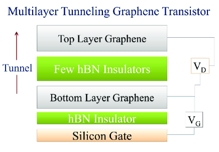
The underlying mechanism Britnell is as follows (cf. Figure 19 for a diagrammatic representation). The Fermi levels and potential barriers are controlled by an applied gate voltage . An electron tunnels between the two graphene layers, only when an electric field (drain-source voltage) is applied, and is sufficiently high to overcome the barrier. When the gate voltage is applied between the silicon gate and the bottom graphene layer, charge carriers in the top and bottom graphene layers begin to accumulate. The Fermi level is raised, and the DoS increases at the same time. Together with the potential difference between the two graphene layers, electrons will be more likely to tunnel form one graphene layer to another. Not only does the applied gate voltage change the DoS, but also modifies the potential barriers between the graphene and insulating layers Britnell . Therefore, a tunneling current through hBN layers is induced, and can be tuned by the magnitude of . Britnell et al. Britnell have also found that the transport carriers are holes. The report also reveals that a larger and separation of the layers would also enhance the switching ratio. The tunneling nature would also allow the transistor to operate at high frequency, as well as with a high current-gain (cf. for details, Georgiou et al. Georgiou ).
VI.8 Radio Frequency Transistor
One can create a band-gap in graphene via any of the aforementioned methods. Even if the band-gap is open, generally, the switching ratio is very small. This is one of the major drawbacks of graphene logic transistors. However, this is no problem for an operational amplifier, or in high-frequency circuits Schwierz ; Kim2 . An amplifying transistor, in general, only requires an ON state. This is because an amplifier requires only a current/voltage input for its operation - thus no OFF state is required. Schwierz . The high mobility of carriers in graphene renders a fast response to the input signal, which can be up to a few hundred GHz, (cf. for details Kim2 ; Lin ; Wu2 ; Zheng ). More specifically, the cut-off frequency and the maximum oscillation frequency both determine the speed of a transistor Kim2 . This maximum oscillation frequency refers to the unity power-gain Wu2 . The cut-off frequency, however, is defined by a current-gain equal to one Wu2 , and is proportional to the trans-conductance .
| (12) |
where is the transistor gate length. To reach a high value for , one has to maximise and minimise Schwierz ; Kim2 ; Wu2 . Wu et al. Wu2 have studied the shortest gate length down to 40nm with a cut-off frequency of 155 GHz. Zheng et al. Zheng have also found, via simulation, that the maximum cut-off frequency can reach up to 300 GHz. On the other hand, impurities and defects would not only downgrade the value of , but the maximum oscillation frequency as well Kim2 . Wu et al. Wu2 also mention that the power-gain in the graphene transistor is particularly low because of the unstable saturation region, of which at present, not much is understood. They add that the maximum oscillation frequency would generally be affected by the size and configuration of the device. Wu et al. Wu2 have also reported that can reach upwards of 20 GHz. It is important to note that the speed of the graphene transistor is influenced by the saturation of the drain current (cf. recent studies by Schwierz ; Wu2 ; Meric ). As previously mentioned, the contact resistance between the metallic materials and graphene is hugely problematic, and even more serious than the undefined saturation drain current Kim2 ; Wu2 . Researchers are looking for further developments to minimise this resistance.
VII Further Developments and Conclusion
Indeed, a long road lies ahead to implement electronic graphene devices into industry. One of the main reasons is that we cannot maintain both the quantity and quality of graphene devices simultaneously throughout the manufacturing processes. For example, mechanical exfoliation can produce high quality graphene flakes, but only a small amount each time. Chemical vapor deposition and evaporation of silicon carbide are able to mass produce graphene substrates - however, these methods require very high temperatures which may sometimes burn out the graphene structure. It is of utmost importance to develop more precise fabrication techniques to reduce the impurities and defects of graphene products Novoselov5 . Most current research is based in laboratories at huge financial expense. How to minimise the spending cost is the next issue to be overcome.
It is highly important to open up a band-gap for the graphene switching devices, of which existing methodologies include carbon nanotubes Behabtu , graphene nanoribbons, deformed structures and bilayer graphene. However, this normally leads to a downgrading of the mobility. One of the major problems for the graphene transistor is current leakage, and the absence of a well-defined ON/OFF switching ratio. The tunneling transistor Britnell may be an innovative solution to this problem, in that it consumes less power and operates at a faster speed. Graphene can also be used in high-frequency amplifiers which do not require a well-defined switching ratio. A recent theory reveals that speeds could even reach upwards of 1THz for photonic devices Kim2 , although one must be careful with regards to the huge contact resistance and unknown saturation regions of a graphene transistor. Some new concepts, such as the single electron transistor and quantum dot transistor, are of great interest, and are being applied to graphene in current research Behabtu ; Lansbergen ; Westervelt ; Ihn . Some research groups are now looking for more stable two-dimensional materials, such as graphyne and silicene O'Hare ; Malko ; Drummond , both of which also possess very good mobility. Both O’Hare et al.O'Hare and Drummond et al. Drummond further mention that the band-gap in silicene can be tuned by an applied electric field. Nonetheless, for now, graphene remains a the forefront for understanding the nanoscale effects of the future generation of transistors Britnell2 .
References
- (1) K. S. Novoselov et al., Electric field effect in atomically thin carbon films, Science 306 (2004), pp. 666-669.
- (2) A.K. Geim, Graphene: status and prospects, Science 324 (2009), pp. 1530-1534.
- (3) A. K. Geim, Graphene prehistory, Phys. Scr. T146 (2012), p.014003.
- (4) A. K. Geim and K. S. Novoselov, The rise of graphene, Nature Mater. 6 (2007), pp. 183-191.
- (5) J. C. Meyer, The structure of suspended graphene sheets, Nature 446 (2007), pp. 60-63.
- (6) A. O’Hare, F. V. Kusmartsev and K. I. Kugel, A stable flat form of two-dimensional crystals: could graphene, silicene, germanene be minigap semiconductors, Nano Lett. 12 (2012), pp. 1045-1052.
- (7) A. O’Hare, F. V. Kusmartsev, K. I. Kugel, Stable forms of two-dimensional crystals and graphene, Physica B-Cond. Matt., 407 (2012), pp.1964-1968.
- (8) L. Tapaszto, T. Dumitrica, S. J. Kim, P. Nemes-Incze, C. Hwang and L. P. Birol, A stable flat form of two-dimensional crystals: could graphene, silicence, germanene be minigap semiconductors, Nature Phys. 8 (2012), pp. 739-742.
- (9) N. D. Drummond, V. Zolyomi and V. I. Fal’ko, Electrically Tunable Band Gap in Silicene, Phys. Rev. B 85 (2012), p. 075423.
- (10) V. Fal’ko, Graphene: Quantum information on chicken wire, Nature Physics 3 (2007), pp. 151-152.
- (11) K. S. Novoselov, Two-dimensional gas of massless Dirac fermions in graphene, Nature 438 (2005), pp. 197-200.
- (12) A. H. C. Neto and K. S. Novoselov, New directions in science and technology: two-dimensional crystals, Rep. Prog. Phys. 74 (2011), p. 082501 .
- (13) S. Chen, Thermal conductivity of isotopically modified graphene, Nature Mater. 11 (2012), pp. 203-207.
- (14) J. Rafiee, Wetting transparency of graphene, Nature Mater. 11(2012), pp. 217-222 .
- (15) K. S. Novoselov et al., Room-temperature quantum hall effect in graphene, Science 315 (2007), p. 1379.
- (16) M. I. Katsnelson, Graphene: carbon in two dimensions, Materials Today 10 (2007), pp. 20-27.
- (17) A. Pototsky, F. Marchesoni, F.V. Kusmartsev, P. Hanggi and S. E. Savel’ev, Relativistic Brownian motion on a graphene chip, European Physical Journal B 85 (2012), p. 356.
- (18) V. V. Zalipaev, D. N. Maksimov, C. M. Linton and F.V. Kusmartsev, Spectrum of localized states in graphene quantum dots and wires, Phys. Lett. A 377 (2013), pp. 216-221.
- (19) C. R. Dean et al., Multicomponent fractional quantum hall effect in graphene, Nature Phys. 7 (2011), pp. 693-696.
- (20) B. Trauzettel, D. Bulaev, D. Loss and G. Burkard, Spin qubits in graphene quantum dots, Nature Phys. 3 (2007), pp. 192-196.
- (21) A. M. Zagoskin, Quantum Engineering: Theory and Design of Quantum Coherent Structures. Cambridge University Press (2011).
- (22) Y. Iyechika, Application of graphene to high-speed transistors: expectations and challenges, Science and Technology Trends - Quarterly Review 37 (2010), pp. 76-92.
- (23) N. Savage, Super Carbon, Nature 483 (2012), S30-S31.
- (24) P. R. Wallace, Band theory of graphite, Phys. Rev. 71 (1947), pp. 622-634.
- (25) D. R. Dreyer, R. S. Ruoff and C. W. Bielawski, From conception to realization: an historical account of graphene and some perspectives for its future, Angew. Chem. Int. Ed. 49 (2010), pp. 9336-9344.
- (26) V. G. Ruess and F. H. Vogt, Hochstlamellarer Kohlenstoff aus Graphitoxyhydroxyd, Monatshefte fr Chemie 78 (1948), pp. 222-242.
- (27) H. P. Boehm, A. Clauss, G. O. Fischer and U. Hofmann, Das Adsorptionsverhalten Sehr Dunner Kohlenstoff-Folien, Z. Anorg. Allg. Chem. 316 (1962), pp. 119-127.
- (28) H. P. Boehm, A. Clauss, U. Hofmann and G. O. Fischer, Dunnste Kohlenstoff-Folien, Zeitschrift Fur Naturforschung Part B-Chemie Biochemie Biophysik Biologie Und Verwandten Gebiete. B 17 (1962), pp. 150-153.
- (29) H. R. Gall, E. V. Rutkov and A. Y. Tontegode, Two dimensional graphite films on metals and their intercalation, Int. J. Mod. Phys. B 11 (1997), pp. 1865-1911.
- (30) C. Berger et al., Ultrathin epitaxial graphite: 2d electron gas properties and a route toward graphene-based nano-electronics, J. Phys. Chem. B 108 (2004), pp. 19912-19916.
- (31) M. L. Sadowski, G. Martinez, M. Potemski, C. Berger and W. A. de Heer, Magneto-spectroscopy of epitaxial few-layer graphene Solid State Comm. 143 (2007), pp. 123-125.
- (32) S. Novoselov et al., Two-dimensional atomic crystals, PNAS 102 (2005), pp. 10451-10453.
- (33) J. Bardeen and W. H. Brattain, The transistor, a semiconductor triode, Phys. Rev. 74 (1948), pp. 230-231.
- (34) F. Schwierz, Graphene transistors, Nature Technology 5 (2010), pp. 487-496.
- (35) K. V. Emtsev et al., Towards wafer-size graphene layers by atmospheric pressure graphitization of silicon carbide, Nature Mater. 8 (2009), pp. 203-207.
- (36) W. A. de Heer et al., Epitaxial graphene, Solid State Comm. 143 (2007), pp. 92-100.
- (37) Z. P. Chen, W. Ren, L. Gao, B. Liu, S. Pei and H. Cheng, Three-dimensional flexible and conductive interconnected graphene networks grown by chemical vapor deposition, Nature Mater. 10 (2011), pp. 424-428.
- (38) X. Li et al., Large-area synthesis of high-quality and uniform graphene films on copper foils, Science 324 (2009), pp. 1312-1314.
- (39) K. S. Kim et al., Large-scale pattern growth of graphene films for stretchable transparent electrodes, Nature 457 (2009), pp. 706-710.
- (40) G. Hlawacek et al., Imaging ultra-thin layers with helium ion microscopy: utilizing the channeling contrast mechanism, Beilstein J. Nanotechnol. 3 (2012), pp. 507-512.
- (41) J. A. Robinson et al. Correlating raman spectral signatures with carrier mobility in epitaxial graphene: a guide to achieving high mobility on the wafer scale, Nano Lett. 9 (2009), pp. 2873-2876.
- (42) A. Ben Gouider Trabelsi, A. Ouerghi, O.E. Kusmartseva, F.V. Kusmartsev, M. Oueslati, Raman Spectroscopy of four epitaxial graphene layers: Macro-island grown on 4H-SiC (000) substrate and an associated strain distribution, Thin Solid Films 538 (2013), doi: 10.1016/j.tsf.2013.05.093.
- (43) A. Das, S. Pisana, B. Chakraborty, S. Piscanec, S. K. Saha, U. V. Waghmare, K. S. Novoselov, H. R. Krishnamurthy, A. K. Geim, A. C. Ferrari and A. K. Sood, Monitoring Dopants by Raman Scattering in an Electrochemically Top-Gated Graphene Transistor, Nature Nanotechnol. 3, (2008), pp. 210-215.
- (44) S. Bae et al., Roll-to-roll production of 30-inch graphene films for transparent electrodes, Nature Nanotechnol. 5 (2010), pp. 574-578.
- (45) J. H. Chen, C. Jang, S. Xiao, M. Ishigami and M. S. Fuhrer, Intrinsic and extrinsic performance limits of graphene devices on , Nature Nanotechnol. 3 (2008), pp. 206-209.
- (46) K. I. Bolotin et al., Ultrahigh electron mobility in suspended graphene, Solid State Commun. 146 (2008), pp. 351-355.
- (47) X. Du, I. Skachko, A. Barker and E. Y. Andrei, Approaching ballistic transport in suspended graphene, Nature Nanotechnol. 3 (2008), pp. 491-495.
- (48) S. V. Morozov et al. Giant intrinsic carrier mobilities in graphene and its bilayer, Phys. Rev. Lett. 100 (2008), p. 016602.
- (49) F. V. Kusmartsev and A. M. Tsvelik, Semi-metallic properties of a heterojunction, JETP Lett. 42 (1985), pp. 257-260.
- (50) H. S. Song et al., Origin of the relatively low transport mobility of graphene grown through chemical vapor deposition, Sci. Rep. (Nature) 2 (2012), p. 337.
- (51) S. D. Sarma, S. Adam, E. H. Hwang and E. Rossi, Electronic transport in two-dimensional graphene, Rev. Mod. Phys. 83 (2011), pp. 407-470.
- (52) Y. B. Zhou, H. C. Wu, D. P. Yu, and Z. M. Liao, Magnetoresistance in graphene under quantum limit regime, Appl. Phys. Lett. 102, (2013), p. 093116.
- (53) S. Datta, Electronic Transport in Mesoscopic Systems, Cambridge: Cambridge University Press (1997).
- (54) M. E. Pumarol et al., Direct nanoscale imaging of ballistic and diffusive thermal transport in graphene nano-structures, Nano Lett. 12 (2012), pp. 2906-2911.
- (55) R. Prasher, Graphene spreads the heat, Science 328 (2010), pp. 185-186.
- (56) A. A. Balandin et al., Superior Thermal conductivity of Single-Layer Graphene, Nano Lett. 8 (2008), pp. 902-907.
- (57) J. H. Seol et al., Two-Dimensional Phonon Transport in Supported Graphene, Science 328 (2010), pp. 213-216.
- (58) Y. K. Koh, M. H. Bae, D. G. Cahill and E. Pop, Heat conduction across monolayer and few-layer graphenes, Nano Lett. 10 (2010), pp. 4363-4368.
- (59) R. R. Nair et al., Fine structure constant defines transparency of graphene, Science 320 (2008), pp. 1308-1308.
- (60) F. Bonaccorso, Z. Sun, T. Hasan and A. C. Ferrari, Graphene photonics and optoelectronics, Nature Photonics 4 (2010), pp. 611-622.
- (61) R. J. Stoehr, R. Kolesov, J. Pflaum, J. and J. Wrachtrup, Fluorescence of laser created electron-hole plasma in graphene, Phys. Rev. B 82 (2010), p. 121408.
- (62) M. Breusing, C. Ropers and T. Elsaesser, Ultrafast carrier dynamics in graphite, Phys. Rev. Lett. 102 (2009), p. 086809.
- (63) T. Kampfrath, L. Perfetti, F. Schapper, C. Frischkorn and M. Wolf, Strongly coupled optical phonons in the ultrafast dynamics of the electronic energy and current relaxation in graphite, Phys. Rev. Lett. 95 (2005), p. 187403.
- (64) M. Lazzeri, S. Piscanec, F. Mauri, A. C. Ferrari and J. Robertson, Electronic transport and hot phonons in carbon nanotubes, Phys. Rev. Lett. 95 (2005), p. 236802.
- (65) V. V. Zalipaev, D. M. Forrester, C. M. Linton and F. V. Kusmartsev, in the book New Progress on Graphene Research, Localised States of Fabry-Perot Type in Graphene Nano-Ribbons, (http://www.intechopen.com/books/new-progress-on-graphene-research) INTECH, (2013), Ch. 2.
- (66) Z. Jiang, Y. Zhang, Y. W. Tana, H. L. Stormer and P. Kim, Quantum Hall effect in graphene, Solid State Comm. 143 (2007), pp. 14-19.
- (67) M. I. Katsnelson, K. S. Novoselov and A. K. Geim, Chiral tunneling and the klein paradox in graphene, Nature Phys. 2 (2006), pp. 620-625.
- (68) A. Calogeracos, Paradox in a pencil, Nature Phys. 2 (2006), pp. 579-580.
- (69) R. K. Su, G. G. Siu and X. Chou, Barrier penetration and klein paradox, J. Phys A: Math. Gen. 26 (1993), pp. 1001-1005.
- (70) A. Calogeracos and N. Dombey, History and physics of klein paradox, Contemp. Phys. 40 (1999), pp. 313-321.
- (71) R. R. Hartmann, N. J. Robinson, and M. E. Portnoi, Smooth electron waveguides in graphene. Phys. Rev. B, 81 (2010), pp. 245431.
- (72) Z. Wu, Electronic fiber in graphene, Appl. Phys. Lett. 98 (2011), pp. 082117.
- (73) J. R. Williams, T. Low, M. S. Lundstrom, and C. M. Marcus, Gate-controlled guiding of electrons in graphene, Nat. Nanotech. 6 (2011), pp. 222-225.
- (74) C. A. Downing, D. A. Stone, and M. E. Portnoi, Zero-energy states in graphene quantum dots and rings, Phys. Rev. B 84 (2011), p. 155437.
- (75) D. A. Stone, C. A. Downing, M. E. Portnoi, Searching for confined modes in graphene channels: The variable phase method, Phys. Rev. B 86, (2012), p. 075464.
- (76) F.V. Kusmartsev, Fine-Structure and Fractional M/N Aharonov-Bohm Effect, Phys. Rev. B52 (1995), pp. 14445-14456.
- (77) G. L. Yu et al. Interaction phenomena in graphene seen through quantum capacitance, PNAS 110 (2013), pp. 3282-3286.
- (78) J. Xia, F. Chen, J. Li and N. Tao, Measurement of the quantum capacitance of graphene, Nature Nanotech. 4 (2009), pp. 505-509.
- (79) F. Giannazzo, S. Sonde, V. Raineri and E. Rimini Screening length and quantum capacitance ing graphene by scanning probe microscopy, Nano Lett. 9 (2009), pp. 23-29.
- (80) W. Li et al., Density of states and its local fluctuations determined by capacitance of strongly disorder graphene, Scientific Rep. (Nature) 3 (2013), p. 1772.
- (81) S. J. Tans, A. R. M. Verschueren and C. Dekker, Room-temperature transistor based on a single carbon nanotube, Nature 393 (1998), pp. 49-52.
- (82) R. Martel, T. Schmidt, H. R. Shea, T. Hertel and Ph. Avouris, Single- and multi-wall carbon nanotube field-effect transistors, Appl. Phys. Lett. 73 (1998), pp. 2447-2449.
- (83) H. W. Zhu, C. L. Xu, D. H. Wu, B. Q. Wei, R. Vajtai, P. M. Ajayan, Direct Synthesis of Long Single-Walled Carbon Nanotube Strands, Science 296 (2002), pp. 884-886.
- (84) P. Avouris, Z. Chen and V. Perebeinos, Carbon-based electronics, Nature Nanotech. 2 (2007), pp. 605-615.
- (85) E. McCann and V. I. Fal’ko, Symmetry of boundary conditions of the Dirac equation for electrons in carbon nanotubes, Joural of Phys. Cond. Matter, 16 (2004), pp. 2371-2379.
- (86) X. Li, X. Wang, L. Zhang, S. Lee and H. Dai, Chemically derived, ultra-smooth graphene nanoribbon semiconductors, Science 319 (2008), pp. 1229-1232.
- (87) J. Park, S. Nam, M. Lee and C. M. Lieber, Synthesis of monolithic graphene-graphite integrated electronics, Nature materials 98 (2011), p. 082117.
- (88) Q. He, S. Wu, Z. Yin and H. Zhang, Graphene-based electronic sensors, Chem. Sci. 3 (2012), pp. 1764-1772.
- (89) Q. He et al., Transparent, flexible, all-reduced graphene oxide thin film transistors, ACS Nano 5 (2011), p. 082117.
- (90) M. Engel et al., Light matter interaction in a micro-cavity controlled graphene transistor room temperature transistor based on a single carbon nanotube, Nature Commun. 3 (2012), pp. 906-911.
- (91) T. H. Hewett, F. V. Kusmartsev, Extraordinary magnetoresistance: sensing the future, Central European Journal of Physics, 10 (2012), pp 602-608.
- (92) M. N. Rudden and J. Wilson, Element of Solid State Physics, New York Wiley (1993), Ch. 4-6.
- (93) K. Kim, J. Y. Choi, T. Kim, S. H. Cho and H. J. Chung, A role for graphene in silicon-based semiconductor devices, Nature 479 (2011), pp. 338-344.
- (94) J. R. Miller, R. A. Outlaw and B. C. Holloway, Graphene double-layer capacitor with ac line-filtering performance, Science 329 (2010), pp. 1637-1639.
- (95) J. D. Irwin and D. V. Kerns, Introduction to Electrical Engineering, New Jersey: Prentice Hall, (1995), Ch. 8-9.
- (96) R. Turton, The Physics of Solids New York: Oxford University Press, (2000), Ch. 4-6.
- (97) C. Coletti, C. Riedl, D. S. Lee, B. Krauss, L. Patthey, K. von Klitzing, J. H. Smet and U. Starke, Charge neutrality and band-gap tuning of epitaxial graphene on SiC by molecular doping, Phys. Rev. B 81 (2010), p. 235401.
- (98) H. Terrones, R. Lv, M. Terrones and M. S. Dresselhaus, The role of defects and doping 2D graphene sheets and 1D nanoribbons, Rep. Prog. Phys. 75 (2012), p. 062501
- (99) X. Fan, Z. Shen, A. Q. Liu and J. L. Kuo, Band gap opening of graphene by doping small boron nitride domains, Nanoscale 4 (2012), pp. 2157-2165.
- (100) P. P. Shinde and V. Kumar, Direct band gap opening in graphene by BN doping: Ab initio calculations, Phys. Rev. B 84 (2011), p. 125401.
- (101) K. Yan, D. Wu, H. Peng, L. Jin, Q. Fu, X. Bao and Z. Liu, Modulation-doped growth of mosaic graphene with single-crystalline p-n junctions for efficient photocurrent generation, Nature Comm. 3 (2012), p. 1280.
- (102) M. M. Kruczynski, E. McCann and V. I. Fal’ko, Electron-hole asymmetry and energy gaps in bilayer graphene, Semicond. Sci. Technol. 25 (2010), p. 033001.
- (103) D. Gradinar, H. Schomerus and V. Fal’ko, Conductance anomaly near the Lifshitz transition in strained bilayer graphene, Phys. Rev. B. 85 (2012), p. 165429.
- (104) K. Kaasbjerg, K. S. Thygesen and K. W. Jacobsen, Unraveling the acoustic electron-phonon interaction in graphene, Phys. Rev. B 85 (2012), p. 165440.
- (105) M. Jin et al., Graphene oxide thin film field effect transistors without reduction, J. Phys. D: Appl. Phys. 42 (2009), p. 135109.
- (106) F. Kreupl, Carbon nanotubes finally deliver, Nature 484 (2012), pp. 321-322.
- (107) A. D. Franklin et al., Sub-10 nm carbon nanotube transistor, Nano Lett. 12 (2012), pp. 758-762.
- (108) Jang, S. et al. Flexible, transparent single-walled carbon nanotube transistors with graphene electrodes, Nanotech. 21 (2010), p. 425201.
- (109) Y. Yang, G. Fedorov, P. Barbara, S. E. Shafranjuk, B. K. Cooper, R. M. Lewis and C. J. Lobb, Coherent nonlocal transport in quantum wires with strongly coupled electrodes, Physical Review B 87 (2013), p. 045403.
- (110) Y. Zhang et al., Direct observation of a widely tunable band-gap in bilayer graphene, Nature 459 (2009), pp. 820-823.
- (111) L. A. Ponomarenko et al., Tunable metal-insulator transition in double-layer graphene heterostructures, Nature Phys. 7 (2011), pp. 958-961.
- (112) M. A. Ionescu and H. Reil, Tunnel field-effect transistors as energy-efficient electronic switches, Nature 479 (2011), pp. 329-337.
- (113) R. Nandkishore and L. Levitov, Common-path interference and oscillatory Zener tunneling in bilayer graphene p-n junctions, PNAS 108 (2011), pp. 14021-14025.
- (114) P. Michetti, M. Cheli and G. Iannaccone, Model of tunneling transistors based on graphene on sic., Appl. Phys. Lett. 96 (2010), p. 133508.
- (115) P. Zhao, J. Chauhan and J. Guo, Computational study of tunneling transistor based on graphene nanoribbon, Nano Lett. 9 (2009), pp. 684-688.
- (116) Q. Zhang, T. Fang, H. Xing and A. Seabaugh and D. Jena, Graphene nanoribbon tunnel transistors, IEEE Electron Dev. Lett. 29 (2008), pp. 1344-1346.
- (117) X. Yang et al., Graphene tunneling FET and its applications in low power circuit design, GLSVLSI10 Proceedings of the 20th symposium on Great lakes symposium on VLSI (2010), pp. 263-268.
- (118) C. M. Malec and D. Davidovic, Transport in graphene tunnel junctions, J. Appl. Phys. 109 (2011), p. 064507.
- (119) E. Cobas, A. L. Friedman,O. M. J. Erve, J. T. Robinson and B. T. Jonker, Graphene as a tunnel barrier: graphene-based magnetic tunnel junctions, Nano Lett. 12 (2012), pp. 3000-3004.
- (120) L. Britnell et al., Field-effect tunneling transistor based on vertical graphene heterostructures, Science 335 (2012), pp. 947-950.
- (121) T. Georgiou et al., Vertical field-effect transistor based on graphene-WS2 heterostructures for flexible and transparent electronics, Nature Nanotech. 8 (2013), pp. 100-103.
- (122) Y. M. Lin et al., 100-GHz transistors from wafer-scale epitaxial graphene, Science 327 (2010), p. 662.
- (123) Y. Wu et al., High-frequency, scaled graphene transistors on diamond-like carbon, Nature 472 (2011), pp. 74-78.
- (124) J. Zheng et al., Sub-10 nm gate length graphene transistors: operating at terahertz frequencies with current saturation, Scientific Rep. 3 (2013), p. 1314.
- (125) I. Meric et al., Current saturation in zero-band-gap, top-gated graphene field-effect transistors, Nature Nanotech. 3 (2008), pp. 654-659.
- (126) K. S. Novoselov, V. I. Fal’ko, L. Colombo, P. R. Gellert, M. G. Schwab and K. Kim, A roadmap for graphene, Nature 490 (2012), pp. 192-200.
- (127) N. Behabtu et al., Strong, light, multifunctional fibers of carbon nanotubes with ultrahigh conductivity, Science 339 (2013), pp. 182-186.
- (128) G. P. Lansbergen, Transistors arrive at the atomic limit, Nature Nanotech. 7 (2012), pp. 209-210.
- (129) R. M. Westervelt, Graphene nanoelectronics, Science 320 (2008), pp. 324-325.
- (130) T. Ihn et al., Graphene single-electron transistors, Materialstoday 13 (2010), pp. 44-50.
- (131) D. Malko, C. Neiss, F. Vines and A. Gorling, Competition for Graphene: Graphynes with Direction-Dependent Dirac Cones, Phys. Rev. Lett. 108 (2012), p. 086804.
- (132) L. Britnell et al., Resonant tunnelling and negative differential conductance in graphene transistors, Nature Comm. 4:1974 (2013).