Theory of local electric polarization and its relation to internal strain: impact on the polarization potential and electronic properties of group-III nitrides
Abstract
We present a theory of local electric polarization in crystalline solids and apply it to study the case of wurtzite group-III nitrides. We show that a local value of the electric polarization, evaluated at the atomic sites, can be cast in terms of a summation over nearest-neighbor distances and Born effective charges. Within this model, the local polarization shows a direct relation to internal strain and can be expressed in terms of internal strain parameters. The predictions of the present theory show excellent agreement with a formal Berry phase calculation for random distortions of a test-case CuPt-like InGaN alloy and InGaN supercells with randomly placed cations. While the present level of theory is appropriate for highly ionic compounds, such as III-N materials, we show that a more complex model is needed for less ionic materials, such as GaAs, in which the strain dependence of Born effective charges has to be taken into account. Moreover, we provide ab initio parameters for GaN, InN and AlN, including hybrid functional values for the piezoelectric coefficients and the spontaneous polarization, which we use to accurately implement the local theory expressions. In order to calculate the local polarization potential, we also present a point dipole method. This method overcomes several limitations related to discretization and resolution which arise when obtaining the local potential by solving Poisson’s equation on an atomic grid. Finally, we perform tight-binding supercell calculations to assess the impact of the local polarization potential arising from alloy fluctuations on the electronic properties of InGaN alloys. In particular, we find that the large upward bowing with composition of the InGaN valence band edge is strongly influenced by local polarization effects. Furthermore, our analysis allows us to extract composition-dependent bowing parameters for the energy gap and valence and conduction band edges.
I Introduction
Electrostatic built-in fields arising from discontinuities of the electric polarization vector significantly modify the electronic and optical properties of semiconductor nanostructures. ambacher_2002 ; bester_2006 ; beya_2011 ; caro_2012 Of particular interest are systems such as GaAs-based quantum dots (QDs), whose electronic and optical properties are affected by the symmetry of strain and strain-induced piezoelectric fields. grundmann_1995 ; schulz_2011 The effect of built-in electrostatic fields is even more dramatic in III-N-based heterostructures, where the large piezoelectric response together with the intrinsic spontaneous polarization give rise to built-in electrostatic fields far exceeding those encountered for other III-V materials. takeuchi_1997 ; ambacher_2002 ; kim_2007 ; lee_2010 ; caro_2011 ; schulz_2010 ; williams_2009 Although these effects have been studied over the last two decades, the possible role of the local polarization potential has only recently been considered. caro_2012
Theoretical studies that include a treatment of polarization fields effectively treat the field at a continuum level (even if the strain itself is obtained from an atomistic calculation), with the polarization assumed to have a smooth behavior with local strain and composition, even in the case of alloys. We have previously shown for InGaN alloys that a local value of polarization can be obtained, observing large fluctuations in its value at a microscopic scale. caro_2012 In this paper we lay our theory of local polarization on more solid ground, giving general equations and providing a direct link with internal strain. We provide a complete and consistent set of polarization-related ab initio parameters for the group-III nitrides, which are needed for the computation of the local and macroscopic contributions to the total polarization. In order to compute the electric potential arising from the local polarization, we also present a “point dipole” method.
When computing the electronic properties of alloyed materials, it is of vital importance that the supercell used allows to reproduce the different configurations encountered in actual material samples. In practice, this implies that the supercell must be sufficiently large. At present, calculations for such large systems escape the reach of ab initio techniques, such as density functional theory (DFT). Moreover, standard implementations of DFT fail to correctly describe band gaps, perdew_1983 and those implementations that allow an accurate prediction of this quantity, such as hybrid approaches, seidl_1996 are computationally much more expensive. On the other hand, alternative semiempirical electronic structure methods enable access to the electronic properties of large systems for which first-principles approaches cannot be realistically implemented. The tight-binding approximation allows an accurate description of the electronic structure in these cases, with the advantage that polarization potentials and deformation potentials can be included as on-site corrections to the Hamiltonian matrix elements. klimeck_2007 ; klimeck_2007b We therefore apply the tight-binding scheme in this work in order to get insight into how the strong local polarization effects influence the electronic structure of InGaN alloys.
The paper is organized as follows. In Section II we introduce the theoretical foundations of the present theory of local electric polarization and discuss its degree of validity. In particular, we show in Section II.3 by comparing our local polarization results to DFT calculations that the first-order level of description presented here works remarkably well in the case of group-III nitrides (relevant ab initio parameters for GaN, AlN and InN are given in Section II.3.1). In Section III we present a point dipole method for the computation of the local polarization potential on an atomic grid, and discuss practical considerations regarding the implementation of the method. Practical examples of the calculation of local polarization and local polarization potential are given in Section IV for polar and non polar InGaN/GaN quantum wells (QWs). In Section V we present a tight-binding (TB) model for the calculation of the electronic structure in nitride systems, and discuss how the local polarization potential affects the band gap of InGaN. We then extract composition-dependent bowing parameters for the band gap and for both the conduction band (CB) and valence band (VB) edges of InGaN alloys over the whole composition range in Section VI. Finally, we summarize our conclusions in Section VII.
II Theory of local electric polarization
When treating a periodic crystal, it is usual to work in terms of the dipole moment per unit volume, that is, the density of dipole moment, or polarization. Crystals whose symmetry allows an inversion centre cannot present a net dipole moment. nye_1985 For crystals without an inversion centre, except point group 432,*[432istheHermann-Mauguinsymbol;usingtheSchoenfliessystem; theequivalentpointgroupis$O$(orthorhombicsymmetry).Whilepointgroup432doesnotpresentlinearpiezoelectricity; Grimmerhasshownthatitiscompatiblewithsecond-orderpiezoelectricity.See][.]grimmer_2007 certain deformations of the crystal lattice give origin to net dipole moments, known as the piezoelectric effect. In addition to this, the subset of those crystals that present an anisotropic direction in the lattice, called polar, are compatible with the existence of net dipoles even in the unstrained state, which is referred to as spontaneous polarization. The wurtzite (WZ) crystal structure belongs to the latter class and therefore WZ nitrides present both piezoelectric and spontaneous polarization. nye_1985
The piezoelectric response of a material to strain is modeled, in the linear regime,111One can also define a second-order piezoelectric tensor to characterize piezoelectricity further away from equilibrium. See Ref. grimmer_2007, via the piezoelectric tensor :
| (1) |
where are the components of the piezoelectric polarization vector and are the strains, given in Voigt notation.222Note that in Voigt notation, , , , , and . The symmetry of the crystal determines the non-zero elements of . We shall see further on that, even for a bulk binary compound, one can define a local piezoelectric tensor whose average over the unit cell reduces to , but that has in general more non-zero elements than . The total polarization vector is given by
| (2) |
where are the components of the spontaneous polarization vector, that will be present only if the crystal symmetry allows, as previously discussed.
Calculating the polarization of a periodic crystal might seem at first a trivial problem, with a possible intuitive definition being given by the charge density of the unit cell. However, there is no way of unambiguously defining the polarization vector using such a method, with an array of possible values arising from different choices of origin. resta_2007 A rigorous frame for the computation of polarization in periodic solids was not available until as recently as the 1990s. The main developments were presented in the seminal papers by Vanderbilt and King-Smith, king-smith_1993 ; vanderbilt_1993 building up on an idea originally suggested by Resta, resta_1992 where the foundations of the Berry-phase theory of polarization, or modern theory of polarization, resta_1994 were laid. This theory allows a calculation of the dipole moment of the unit cell of a periodic insulating system, which is well defined modulo (where is the elementary charge and R is a lattice vector). The latter ambiguity can be removed in different ways, such that a meaningful value for the polarization can be obtained. king-smith_1993 ; vanderbilt_1993 ; bernardini_1997 However, the obtainment of a position-dependent polarization vector, that varies within the unit cell in which the Berry phase is computed, is beyond the reach of this technique. Nevertheless, for systems where composition and/or strain change abruptly within the unit cell (e.g. random alloy InGaN QWs), the question of whether a local value of the polarization vector can be calculated becomes pertinent.
In the context of the Berry-phase technique, only the average polarization of the periodic unit cell as a whole can be calculated formally. In a general calculation, there may not necessarily be an obvious or straightforward way to partition the system into subsets for which the polarization can be easily computed in separate calculations. Any knowledge of how the polarization varies within the supercell must therefore rely on a heuristic assumption. This motivates to find a phenomenological solution to the problem, to gain access to physical information which would not be accessible otherwise. We show below that, within the present local polarization formalism, a position-dependent polarization, defined down to the unit volume of an ensemble of nearest-neighbors, yields results in good agreement with a formal Berry-phase calculation, when extrapolated to calculate the average polarization of the supercell. This agreement provides strong support that the approach presented here provides an accurate description of local polarization effects in III-N heterostructures and alloys.
II.1 Formal definition of the local polarization
As already discussed, the total macroscopic polarization has two components: spontaneous and piezoelectric. Because the spontaneous polarization is a reference state, establishing a local value for it formally might prove rather non trivial: one would need to devise an adiabatic transformation which keeps the system insulating while moving from an equivalent centrosymmetric structure to the polar crystal structure that allows to evaluate the difference in polarization locally (at each atomic site). resta_2007 Therefore, to avoid this complexity, we assume the spontaneous polarization for a given binary compound to be position-independent and direct our attention towards the piezoelectric polarization instead.
Our aim is a reformulation of Eq. (1) that allows an evaluation of the local and macroscopic contributions to the polarization separately. For the sake of clarity and conciseness, we constrain ourselves to changes in that are linear in the strains. Future work will extend our description to second-order piezoelectric polarization. As we will see later on, the linear approximation breaks down quickly for some III-Vs but is good up to moderate strain for the highly ionic III-nitrides. In analogy to elasticity, caro_2013 we can generalize Eq. (1) for arbitrary internal strains as follows:
| (3) |
where is the number of atoms in the unit cell, is the component of the internal strain vector for atom , is the elementary charge, is the volume of the unit cell, and is the component of the Born effective charge tensor gonze_1997 for atom . are the internal strains that minimize the total energy of the crystal for any given strain state . caro_2013 Although Eq. (3) is general, because we are working in the linear approximation we will assume that the off-diagonal components of the Born effective charges are zero. Equation (3) therefore reduces to
| (4) |
where we have employed an implicit notation . Again, in the linear limit, the are linear in and we can write
| (5) |
where is the piezoelectric coefficient obtained from a “clamped-ion” calculation, bernardini_1997 in which the ionic coordinates are not allowed to relax. Note that in Eq. (5), the first term is macroscopic, that is, defined for the unit cell as a whole, while the second one is evaluated locally.
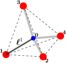
Consider now that is the volume comprising an atomic site and all of its nearest neighbors (in the context of the four-fold coordinated ZB and WZ lattices this would correspond to each of the tetrahedra that make up the crystal). We label the central atomic site 0 and each of its nearest neighbors by . Then, the relevant quantity in Eq. (5) to be evaluated locally (at the atomic site 0) is
| (6) |
where is the number of nearest neighbors of atom . By dividing the contribution of each of the nearest neighbors by their own number of nearest neighbors we ensure no double counting when extending the evaluation of Eq. (6) to the whole crystal.
The internal strains can be obtained in a relatively straightforward manner for binary compounds. caro_2012c ; caro_2013 However, for an irregular material, such as an alloy, establishing a reference lattice structure with respect to which the internal strains could be calculated would carry a high degree of arbitrariness. Furthermore, an exact evaluation of Eq. (6) would rely on knowing the value of for all the atoms present in the crystal. For an irregular material, would differ, in general, for each atom, even (by a small amount) for atoms of the same species. Therefore, our choice is to deduce an approximation to Eq. (6) valid for a representative reference system (such as a binary), and use that approximation to estimate the local polarization in irregular systems. We propose the following spherical approximation for the local environment of the central atom (atomic site 0):
| (7) |
The approximation given by Eq. (7) would be exact if all the nearest neighbors () of atom 0 were piezoelectrically equivalent, that is, if all of them have the same Born effective charges. This is the case for binary ZB and WZ compounds. Further on, we will deal with how different approximations work out for alloys.
We can characterize the bonds between atom 0 and atoms by a vector as indicated in Fig. 1. If is the bond vector of the unstrained case, we can write in terms of the macroscopic and internal strains:
| (8) |
where are the components of the strain tensor in Cartesian notation and is the Kronecker delta function. With the approximation of Eq. (7) and the definition given by Eq. (8) we rewrite Eq. (5) as
| (9) |
where , defined as a summation over nearest-neighbor distances, is the bond asymmetry parameter. caro_2012 is the bond asymmetry parameter of the unstrained system, that would be zero for binary ZB materials and would have a non-zero component along the polar axis for WZ materials. caro_2012
Finally, we write for the total polarization at atomic site 0:
| (10) |
Equation (10) is a central result of this paper, which separates the contributions to the polarization arising from macroscopic effects, given by the clamped-ion piezoelectric coefficient , and local effects, dominated by internal strain.
II.2 Validity of the model
We have made a number of approximations in the previous section. Depending on the nature of the compound at hand, each of them will have a different impact on the results, and will limit the accuracy that can be achieved. These approximations are:
-
1.
We have assumed that is constant throughout the crystal for binaries. However, we have defined it as a local quantity (this will prove helpful when dealing with alloys).
-
2.
For the piezoelectric part, we have truncated our description to first order in both macroscopic and internal strain.
-
3.
We have assumed that the off-diagonal terms of the Born effective charge tensor are zero.
-
4.
We have performed a spherical approximation for the Born effective charge of the nearest neighbors of the atom where the local polarization is evaluated.
As discussed in Section II.1, it is not trivial to establish whether approximation 1 is good or not. It is possible to separate the contributions to into that arising from the initial bond asymmetry parameter that we have defined previously (which in WZ is related to the internal parameter ), and the purely electronic contribution of the ideal WZ lattice. caro_2012 ; bernardini_2001 ; pal_2011 In this context, it is possible to assign a local value for the initial bond asymmetry contribution, which in the case of WZ would be equal in both cation and anion sites. It seems therefore that assuming the electronic part to be also constant between different atomic sites for the binaries might be reasonable.
Approximation 2 is indeed the main limitation to the model introduced here, but possibly the most straightforward one to overcome. The theory can be extended to include second-order piezoelectric effects at the expense of complicating the formulas. We opt here to limit ourselves to a first-order description to emphasize the conceptual implications of the theory. The linear limit should be valid for highly ionic compounds, such as group-III nitrides, as will be shown in the next section. For the nitrides, although the second-order effects are large, the first-order terms dominate up to strain values that are typically found in realistic alloys and heterostructures (up to 5%). ambacher_2002 ; fiorentini_2002 ; caro_2011 ; prodhomme_2013 However, for other III-V materials, second-order piezoelectric coefficients are relatively much larger compared to the linear ones. For instance, for the Al compounds AlP, AlAs and AlSb, Beya-Wakata et al. beya_2011 found that the first-order piezoelectricity can practically be neglected and second-order effects dominate even for small strains. For GaAs the situation is intermediate and the present level of theory should be accurate for small strains below 1 or 2 %. This complication is also present when computing the Born effective charges. As we show in Fig. 2 for the hydrostatic and biaxial strain dependence of (see figure caption and next section for details of the calculation), the linear approximation for the Born effective charge gets worse as one moves from highly ionic AlN to the less ionic materials GaAs and AlAs. Note that strain-dependent Born effective charges also have an impact on the clamped-ion piezoelectric coefficient, as given by Eq. (5). Therefore, a more complete and accurate treatment for general materials should eventually include the dependence of the Born effective charge on strain. Note that within this linear model, the contributions of clamped-ion terms and Born effective charges are assumed linear in the strains in the formal derivation of the formulas. However, the formalism does not impose a linear dependence of internal strain upon macroscopic strain when calculating the : this dependence is determined by the specific theoretical framework used for the computation of the atomic geometry of the system, e.g. DFT, a valence force field, etc. In the case of nitrides, Prodhomme et al. prodhomme_2013 have found relatively large non-linear effects on binary and ternary compounds. As will be shown in the next section, the present local model succeeds at computing the polarization in nitride ternaries because its main non-linear contribution arises from non-linearities of local internal strain itself, including the effect of disorder.

Approximation 3 is generally good, since for binary compounds the off-diagonal components of the Born effective charge are typically zero, and in any case the ratio is usually small.
The validity of approximation 4 relies greatly on the specific crystalline structure and whether the nearest neighbors of the central atom where the polarization is being calculated are equivalent (that is, have the same Born effective charge) or not. For this reason, in the case of binary tetrahedrally bonded compounds, where all the nearest neighbors for one given site are of the same atomic species, this approximation should be good for small strains. As observed in Fig. 2 for biaxial strain, lattice distortions that change the symmetry of the bonds have a large impact on the Born effective charge for some compounds. Therefore, the validity of Eq. (10) would be limited for low ionicity and the more general form, Eq. (5), should be used. On the other hand, for ionic compounds such as nitrides, Eq. (10) retains its validity and offers an accurate description of the local effects, as will be shown in Section II.3. In both cases (low and high ionicity in tetrahedrally bonded binaries) the approximation is exact for the linear piezoelectric limit (see Section II.3.2).
II.3 Testing the theory for group-III nitrides
As a first validation test and application of the theory, we have chosen group-III nitrides. The III nitrides are technologically important semiconductors for a wide range of optoelectronic applications. nakamura_2000 ; krames_2007 ; mishra_2008 The strong piezoelectric response of nitride compounds, together with the existence of the spontaneous polarization, has a large impact on the electromechanical properties of devices that incorporate them. The large difference in bond lengths between the nitride binaries leads to considerable local strains in these alloys, with measurable effects such as large band gap bowings. wu_2009 ; aschenbrenner_2010 We have previously shown how these local strain fields affect the electric polarization for InGaN alloys, retrieving the macroscopic limit with the advantage of giving a description of the local effects at the same time. caro_2012 We have now presented in Section II a refined and more general form of that model. In the following, we will thoroughly apply this theory to test its validity for III-N materials.
II.3.1 Parameters involved in the calculation of the local polarization
| AlN | GaN | InN | ||||
|---|---|---|---|---|---|---|
| HSE | LDA | HSE | LDA | HSE | LDA | |
| (Å) | 3.103 | 3.092 | 3.180 | 3.154 | 3.542 | 3.507 |
| (Å) | 4.970 | 4.947 | 5.172 | 5.141 | 5.711 | 5.668 |
| 0.3818 | 0.3820 | 0.3772 | 0.3765 | 0.3796 | 0.3787 | |
| 0.138 | 0.145 | 0.156 | 0.168 | 0.193 | 0.204 | |
| 0.086 | 0.091 | 0.083 | 0.089 | 0.107 | 0.112 | |
| 0.191 | 0.200 | 0.159 | 0.168 | 0.218 | 0.226 | |
| 0.199 | 0.224 | 0.201 | 0.210 | 0.337 | 0.339 | |
| 0.143 | 0.140 | 0.141 | 0.148 | 0.107 | 0.118 | |
| (C/m2) | -0.39 | -0.43 | -0.32 | -0.36 | -0.42 | -0.47 |
| (C/m2) | -0.63 | -0.69 | -0.44 | -0.49 | -0.58 | -0.63 |
| (C/m2) | 1.46 | 1.59 | 0.74 | 0.83 | 1.07 | 1.09 |
| (C/m2) | -0.091 | -0.096 | -0.040 | -0.029 | -0.049 | -0.041 |
| (C/m2) | -0.031 | -0.033 | -0.019 | -0.016 | -0.019 | -0.016 |
| (C/m2) | 0.28 | 0.28 | 0.43 | 0.45 | 0.39 | 0.35 |
| (C/m2) | 0.26 | 0.25 | 0.40 | 0.41 | 0.37 | 0.38 |
| (C/m2) | -0.51 | -0.47 | -0.87 | -0.87 | -0.87 | -0.95 |
| 2.53 | 2.52 | 2.64 | 2.58 | 2.85 | 2.83 | |
| 2.68 | 2.67 | 2.77 | 2.72 | 3.02 | 3.00 | |
The first step in setting up the theory is to derive the necessary parameters for the WZ III-N binaries GaN, AlN and InN: piezoelectric tensor , spontaneous polarization , Born effective charges , lattice parameters and , internal parameter , and internal strain parameters . For our calculations we have used the plane wave implementation of density functional theory (DFT) available from the vasp package, ref_vasp ; kresse_1996 within the projector augmented-wave (PAW) method. bloechl_1994 ; kresse_1999 We perform calculations using both the local density approximation (LDA) and the Heyd-Scuseria-Ernzerhof (HSE) screened-exchange hybrid functional. heyd_2003 ; heyd_2004 ; caro_2012c For the LDA calculations we use vasp’s implementation of the Perdew-Zunger parametrization, perdew_1981 while the settings for the HSE functional correspond to HSE06, with mixing parameter and screening parameter . In all calculations the cutoff energy for plane waves is 600 eV. All the quantities involving a calculation of the polarization have been obtained using Martijn Marsman’s implementation of the Berry phase technique vanderbilt_1993 available in vasp. We use HSE to obtain high quality parameters for the binaries and LDA to perform test calculations for larger supercells and for statistical evaluation of the accuracy of the theory. In our experience, LDA-DFT gives a good description of elastic properties and internal strain, while at the same time being computationally affordable. Also, LDA-DFT seems to give results in better agreement with experiments than generalized-gradient approximations (GGAs) for the calculated electric polarization, at least for III-V compounds. beya_2011 The more computationally demanding HSE functional, on the other hand, reduces the band gap problem existent in standard Kohn-Sham DFT, henderson_2011 that potentially leads to a conducting phase being incorrectly predicted for narrow gap semiconductors, such as InN. HSE also provides lattice parameters and elastic properties in better agreement with experiment. caro_2012c
The calculated structural and polarization-related parameters of the III-N binaries are summarized in Table 1. In the context of the Berry phase approach, a meaningful value for the polarization can only be calculated if the system remains insulating. vanderbilt_1993 ; king-smith_1993 ; resta_1994 As already discussed, in the case of the III-N compounds this is not a problem for the HSE functional, which predicts a positive gap. yan_2009 Using the LDA, AlN and GaN are predicted to have (underestimated) positive gaps. However, our settings lead to the prediction of a band crossing at the point for InN, and therefore an incorrect metallic phase that renders the calculation of a meaningful value of the polarization uncertain. Previous data have been given for InN by Fiorentini and collaborators in a series of papers on the piezoelectric properties and spontaneous polarization of group-III nitrides. bernardini_1997 ; bernardini_2001 ; zoroddu_2001 While their LDA calculations obtain the correct insulating phase of InN,333Private communication with V. Fiorentini and D. Vanderbilt. ours must rely on a different approach. Because the band crossing occurs only at the point and immediate surroundings, we skip this area in the -point integration by shifting the k mesh away from . The resulting LDA values of the polarization-related quantities in Table 1 show almost perfect agreement with Fiorentini et al.’s LDA data, bernardini_2001 ; zoroddu_2001 although InN remains technically a metal in our case. The good agreement with the HSE calculation further supports that our LDA values should be correct.
It should be noted that our calculations yield a negative sign for in both the LDA and HSE schemes. Initial measurements muensit_1999 and calculations bernardini_2002b reported a positive value for , as included in Vurgaftman and Meyer’s widely cited review paper. vurgaftman_2003 Our value here is in line with more recent studies and analyses which show that a negative value is required both for agreement with experiment and for internal consistency among the different piezoelectric coefficients. schulz_2009 ; schulz_2011 ; schulz_2012b ; shimada_2006 Very recent LDA calculations of second-order polarization of III-nitrides and ZnO by Prodhomme et al. prodhomme_2013 show good agreement with our linear coefficients of Table 1. The agreement between HSE and LDA highlights the fact that LDA provides reliable values for the electric polarization provided that it also succeeds at predicting reliable band gaps and structural parameters: the largest discrepancies are for the spontaneous polarization of GaN and InN, which are influenced by the discrepancy between HSE and LDA for the calculated value of .
II.3.2 Local piezoelectric tensor
We have previously obtained the relation between macroscopic and internal strain for the WZ lattice and provided the definition of the five WZ internal strain parameters in Ref. caro_2012c, . To obtain the relation between piezoelectric coefficients and internal strain parameters , one can apply Eq. (5) to the internal strain vectors for the WZ geometry. The results can conveniently be expressed in the following compact form:
| (11) |
We have incorporated in Eq. (11) none of the assumptions leading to Eq. (10). Therefore, Eq. (11) is an exact result for WZ crystals in a linear piezoelectric model. It is thus initially surprising that and , although breaking the cell symmetry, do not appear in the expressions for the . The reason for this will become clear when obtaining the as , calculated from Eq. (10).
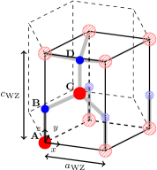
Following the convention of Fig. 3, the local piezoelectric tensor, notated , can be calculated at the atomic sites A and C, corresponding to the two cations present in the unit cell, as the derivative of Eq. (10) with respect to the strains:
| (12) |
where indicates A or C. For a WZ structure, the only non-zero component is . caro_2012 Expressing in terms of macroscopic strains, lattice parameters and internal strain parameters, each of the non-zero components of can be obtained (an example calculation for is given in Appendix A):
| (13) |
That is, the expressions for , and are retrieved exactly, but additional piezoelectric components appear, that change sign going from A to C. To elucidate the effect of this on the symmetry of the piezoelectric tensor, we write in matrix form:
| (17) |
When averaging and within a given unit cell, one retrieves the WZ macroscopic limit:
| (21) |
The anion sites B and D have the same expressions for , and and slightly different expressions for :
| (22) |
The macroscopic limit is of course also retrieved when averaging for the anion sites. Note that the values of are comparable to those of the macroscopic piezoelectric tensor coefficients. For instance, for GaN, amounts to 0.79 C/m2 and 1.13 C/m2 for cation and anion sites, respectively.
Equation (17) is the (site-dependent) local piezoelectric tensor for a WZ lattice. It reflects the fact that there exist two sets of inequivalent tetrahedra in a WZ lattice, and that the macroscopic strain affects the nearest-neighbor environment of each of them differently. caro_2012c ; caro_2013 This is a priori an unexpected result, and implies that crystals that are non-polar and non-piezoelectric on average could nevertheless present a local, perhaps measurable, piezoelectric-like polarization.
Finally, note the similarity between the local piezoelectric tensor of WZ and that of ZB in a (111)-oriented description [Eq. (27) of Ref. schulz_2011, ]. This reflects that (111)-oriented ZB systems present a three-fold symmetry, schulz_2011 where all cation (anion) sites have an equivalent environment, contrary to the WZ case, where there are two inequivalent cation (anion) sites. caro_2012c
II.3.3 Local polarization in InGaN alloys: strategies and testing
| 32-atom supercells | 128-atom supercells | |
|---|---|---|
 |
 |
We have seen so far that for wurtzite nitride binaries there is an exact correspondence between local and macroscopic polarization that is retrieved when averaging the local part over the unit cell. Although some solid-state devices might operate employing binary compounds, the most interesting applications of the nitrides arise through the use of their alloys for controlled variation of properties (e.g. band gap tunability).
The main problem facing a local polarization calculation for an alloy is the increased complexity of the atomic environment of each of the sites where the local polarization is to be evaluated. This is due to the fact that the Born effective charges of all the atoms involved in the calculation are affected by the interaction with all the other atoms present in the crystal. In a periodic cell calculation this number would be reduced to the number of atoms in the supercell. Since there is an arbitrarily large number of possible configurations depending on alloy composition and supercell size, establishing an exact correspondence between local and macroscopic polarization in the fashion of Section II.1 then becomes virtually impossible. To overcome this limitation, we will assume for the nitrides, and InGaN in particular, that the Born effective charge of the cations in the alloy remains the same as for the binary, and that the spherical approximation still holds. caro_2012 We have devised two tests in order to establish how good this approximation is. First, we will use the smallest alloy cell, which is a CuPt-like (CP-like) InGaN unit cell consisting only of 4 atoms, caro_2012 ; bernardini_2001 and will perform random distortions of the atomic positions within the unit cell. The result of the averaged local polarization, calculated using Eq. (10), will be compared to the formal Berry-phase result. Second, 32- and 128-atom In0.5Ga0.5N supercells will be considered and the cation sites occupied randomly with either a Ga or an In atom, with the only requirement that the stoichiometric ratio of 1/1 be preserved (i.e. the nominal composition of all cells is the same). The internal atomic positions will then be allowed to relax by minimizing the supercell LDA-DFT total energy, and the result of the averaged local polarization will again be compared to that of a Berry-phase calculation. The statistical treatment of both tests will reveal the validity of the approximation for InGaN alloys.
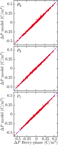
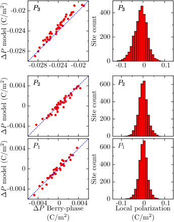
The results of the first test are depicted in Fig. 4. The figure shows a comparison of the average polarization of the CP-like InGaN cell calculated both within the present local polarization model and with the Berry-phase technique. We have performed random displacements of up to (which is equivalent to approximately 10% of the equilibrium bond lengths) to each of the Cartesian coordinates of each of the 4 atoms in the unit cell. For the local polarization model, we have computed the local polarization contributions at the Ga and In sites using Eq. (10) and then obtained its average for the whole cell. Since only differences in polarization are meaningful within the Berry-phase formalism, king-smith_1993 ; vanderbilt_1993 we compare in Fig. 4 the difference between the polarization of the equilibrium CP-like InGaN structure and the distorted one. As can be seen, the agreement between the two methods is excellent, with all the data points lining up against the dashed line that corresponds to perfect agreement .
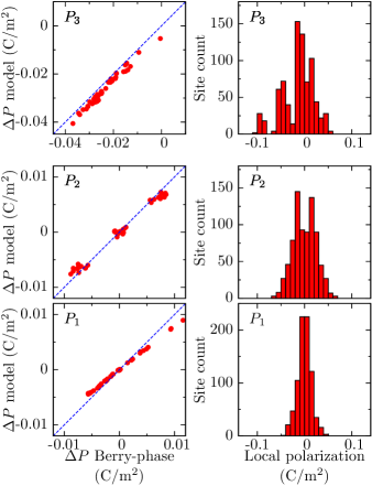
Even more enlightening is the comparison between the present model and the Berry-phase results depicted in Fig. 5 for random In0.5Ga0.5N orthorhombic supercells. In that figure, is the difference between the polarization of the supercell before and after internal strain relaxation. The supercells are constructed with either 32 or 128 atoms and the In and Ga atoms are placed randomly at the cation sites. The lattice vectors of the supercells are kept fixed and chosen as the average between the LDA values for the binaries. The “site count” panels show the number of cation sites that present a particular local polarization value within different ranges, for the combined supercells. We note two main features. The first observation is that the local polarization model succeeds at very accurately predicting the average supercell polarization even though the latter is calculated from a sum over many local contributions whose values vary within limits which are approximately one order of magnitude higher. Second, our results show that the average polarization is highly dependent on the specific atomic arrangement, even for a large number of atoms. Bernardini and Fiorentini bernardini_2001 have previously calculated the spontaneous polarization for the same material using a 32-atom special quasirandom structure (SQS), wei_1990 and have proposed that disorder plays only a secondary role in the calculation of the polarization, both spontaneous and piezoelectric. bernardini_2001 ; bernardini_2002 ; fiorentini_2002 ; ambacher_2002 We have found that this is indeed the case for the spontaneous polarization of the supercells studied before the optimization of the atomic degrees of freedom: all the 128-atom configurations studied yielded the same value of within less than 0.001 C/m2 of each other. However, our results suggest i) that a 32-atom supercell might not be large enough to study the effect of disorder (see e.g. clustering of calculated values for in Fig. 5) and ii) that internal strain relaxation introduces large corrections to the polarization value, even for supercells containing as many as 128 atoms. Note, for instance, that the average in-plane components of the polarization and , which are not symmetry-allowed for the binaries, do not vanish for the alloys in the case of finite-size supercells.
All of these considerations not only support the validity of the local model discussed here, but also highlight the need for one, in order to be able to treat the effects of disorder and associated internal strain accurately.
III Point dipole method for the calculation of the polarization potential
When trying to calculate the local polarization potential by solving Poisson’s equation in the same atomic grid where the polarization is given, one encounters two main difficulties. The first arises from the discretization of the medium, which is irregular given the arrangement of the atoms in the strained crystal. The second, and most important, is a problem of resolution: because Poisson’s equation needs to be solved in a finite difference or polynomial interpolation schemes, and its solution involves the calculation of several derivatives (see, for instance, Ref. bester_2005, ), approximate interpolations have to be made and the effects of abrupt local discontinuities are lost in the process. In order to compute the local polarization potential and overcome these limitations, we have previously used a point dipole model. caro_2012 Here we give the details of our model and extend it, as well as assess its limitations and degree of validity for calculations involving a position-dependent value of the polarization.
The point dipole model is a solution to the challenge of solving Poisson’s equation on an atomic grid where abrupt changes in the polarization vector occur. caro_2012 This is achieved with a method that computes at any arbitrary position the potential contribution due to each dipole individually, without involving the interpolation of quantities between neighboring grid sites that would lead to loss of resolution. However, before the polarization potential can be obtained from the point dipoles, a remapping of polarization density into dipole moment on the system’s grid has to be performed. The latter is dealt with in Section III.1. The general solution for the polarization potential arising from the ensemble of point dipoles is obtained in Section III.2 in an image dipole scheme, for a QW system (or layered structure, in general) where a different arbitrary dielectric constant is allowed for all three neighboring layers of material. The effect of different levels of approximation for this general solution is also treated in Appendix B. In Section III.3 we present a comparison between the solution of Poisson’s equation for a problem with an available analytical solution and different levels of implementation of our method. Further material complementary to this section, including computational aspects, is given in Appendix B.
III.1 From polarization to dipole moment
Before establishing the form of the potential due to a point dipole ensemble, we focus our attention on the transformation between polarization density P, which is the quantity usually calculated in strained crystals, and dipole moment p, which is the quantity involved in the equations that will be presented in the next section.
The polarization P can be understood as a “density of dipole moment”. Indeed, the total dipole moment of a finite size sample in which the polarization density is constant is simply the product of P and the volume of the sample. Therefore, when dealing with constant polarization in a continuum-based description, a standard cubic discretization of the material, with step size , is well suited to the representation of P as an ensemble of dipoles of magnitude located at each of the mesh points. However, our main interest is the representation of the material as an ensemble of point dipoles in an atomistic scheme. For tetrahedrally bonded compounds this involves the discretization in a mesh with either cubic (zinc-blende) or hexagonal (wurtzite) coordination, in the ideally undistorted lattice. After strain is applied, the former grids will suffer a deviation from cubic and hexagonal symmetries and the assignment of a finite volume to each mesh point becomes cumbersome.
In the description of local polarization that we have previously employed, the values of P were given at the sites of each of the cations present in the crystal. caro_2012 The latter is a useful description, in the sense that the representation of the whole crystal as a collection of deformed tetrahedra can be done via the relative positioning of the nearest neighbors: each cation and its four neighboring anions unambiguously define each tetrahedron. Labeling the anions immediately surrounding a cation as 1, 2, 3 and 4 (Fig. 1), we refer to the volume of the corresponding tetrahedron as . If the positions of the anions are , , and , then is given by
| (23) |
However, it can be easily shown that only accounts for the volume of the tetrahedron itself and that a summation of the volumes of all the tetrahedra contained within a material sample would underestimate the volume of the sample by exactly a factor of 6. Therefore, we define the volume corresponding to a tetrahedron as
| (24) |
Now, the value of the dipoles can be easily obtained once a map of the polarization is available. For simplicity, we denote each grid point by and the volume of the corresponding tetrahedron, as given by Eq. (24), as :
| (25) |
with being located at the position of cation .
Our choice for a cation-based description stems from convenience. In a nitride alloy all the anions are nitrogen atoms and therefore applying the spherical approximation of Eq. (7) (which is based on nearest neighbors only) leads to one Born effective charge definition per cation atomic species: Ga, In and Al for conventional III-N. Using an anion-based description would lead, in the case of nitrides, to defining 15 different Born effective charges for N, which correspond to the 15 possible combinations of Ga/In/Al atoms that can be nearest neighbors to N (e.g, 4 Ga, 3 Ga and 1 In, 2 Al and 2 In, etc.).
III.2 Solution for materials with different dielectric constant
Given the multipole expansion of a distribution of electric charge (see, for example, Ref. jackson_1999, ), the contribution to the electrostatic potential calculated at r due to a point dipole p is given by
| (26) |
where is the position of the dipole p, is the permittivity of the vacuum, and is the dielectric constant of the material. Equation (26) is only valid when both the dipole p at and the point r where the potential is calculated are contained within an infinite (or big enough to neglect surface effects) sample of a dielectric material with dielectric constant . For the more general case in which there are boundaries between materials with different dielectric constants, e.g. a quantum well, it is appropriate to use the method of images to obtain a form of Eq. (26) that accounts for the discontinuity of across the different interfaces. The details of the method and the treatment for the case of up to three material layers with different dielectric constants are given in Appendix B.
III.3 Comparison to the solution of Poisson’s equation for simple structures
Polar Non polar
Before applying the model to calculate the local polarization potential in realistic structures, it is necessary to test its accuracy against well established methods. An excellent test is the calculation of the polarization potential in a capacitor-like structure. In such an example, a layer of dielectric material (1) of thickness , in which the polarization (where is a unit vector along the axis) is constant and perpendicular to the neighboring interfaces, is surrounded by two infinite layers of a dielectric material (2), with a different dielectric constant, in which the polarization is zero. An exact analytical solution to Poisson’s equation can be obtained for the latter case. If we assume the first interface is located at , the potential is given by
| (27) |
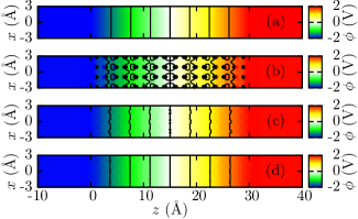
where is the dielectric constant of material (1). Figure 6(a) shows the potential profile as calculated exactly and analytically using Eq. (27) for the special case in which , and , which would be typically the situation in an InGaN QW surrounded by GaN barriers in which, for simplicity, the polarization has been switched off in the barriers. Within this simplified continuum picture, a spatial discretization of the current problem in a cubic grid of steps , as discussed in the previous section, creates an ensemble of point dipoles which are of similar size to the ones encountered in typical InGaN QW situations. The application of our dipole method to first order reflections (see Appendix B) leads to a potential profile as in Fig. 6(b). In that figure, it can be observed how the potential changes brusquely in the surroundings of the dipoles (the plane of the figure has been deliberately chosen to be one that contains dipoles in it to dramatize this effect). This is due to the fact that Eq. (26) is a valid solution for a distribution of charge only if the position where the potential is calculated is sufficiently far away from the location of the point dipole that represents that distribution. We acknowledged this limitation in our previous work and proposed a cutoff radius around r for which only the dipoles that obey the condition are taken into account. caro_2012 The potential profile for the present example and is shown in Fig. 6(c). Although this solution certainly improves the results and leads to a much better agreement with the analytical solution, it has the inconvenience of creating sharp transitions at the cutoff distances around the dipoles. To complement this treatment, we have now substituted the elimination of dipoles below the cutoff radius by a Gaussian smearing of dipoles that obey the condition , as detailed in Section B.2 of Appendix B. This solution leads to smoother potentials and a much better agreement with the analytic solution for this test case, as observed in Fig. 6(d).
IV Selected results for InGaN quantum wells
Once the method for calculating the local polarization potential has been established, we can turn our attention towards achieving a local description of that quantity in relevant nanostructures. In the present example, we look at InGaN/GaN QWs grown along polar and non-polar*[Non-polarQWsstructureshavepreciselybeenproposedasapossiblesolutiontothebuilt-infieldissueinnitrideheterostructures; see][.]paskova_2008 directions. Polar structures are grown along the -axis, whereas in the case of non-polar structures the -axis lies within the growth plane. In a macroscopic picture of the polarization, there are no discontinuities in P between the well and barriers in the non-polar case. However, as we shall see, in a microscopic description discontinuities occur locally, depending on local strain and composition.
Although we used in Section II.3 DFT to optimize the atomic positions of the supercells studied, such an approach is unaffordable for large supercells, given both the computer time and memory usage required. The usual approach to relax the atomic degrees of freedom in such cases is to use a classical interatomic force method. For tetrahedrally bonded compounds, Keating’s valence force field (VFF) model keating_1966 is by far the most popular. pryor_1998 ; camacho_2010 Camacho and Niquet have previously used a modified version of Keating’s model, adapted to the WZ crystal structure, to account for the deviation of the ratio of lattice parameters with respect to its ideal value. camacho_2010 We have instead chosen an approach based on Martin’s VFF martin_1972 that includes the electrostatic interaction explicitly. caro_2012 At a higher computational cost, this model succeeds at predicting the deviation of the ratio while maintaining the correct symmetry of the interatomic interactions. For instance, the two-body interactions directed along the WZ -axis have the same functional form, including the equilibrium bond length, as the other ones. This allows to obtain a much more flexible set of potentials that are transferable between similar polymorphs of the same compound, i.e. WZ and ZB in this case. With our model we are able to predict elastic and structural properties of binary and ternary nitrides in excellent agreement with first-principles DFT calculations, therefore providing solid grounds for using the supercells relaxed using this method as high-quality input for the subsequent local polarization calculation. An extensive article with the details and validity of our method is currently in preparation and will be published elsewhere.
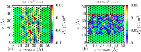
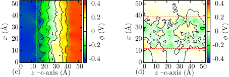
Making use of the expressions derived throughout this chapter, and the VFF just outlined, we have calculated the local polarization for InGaN/GaN QWs with 30% In content in both polar and non-polar orientations, as shown in Figs. 7(a) and (b), respectively. Note that the component shown in the color code is the component of the polarization along the -axis. The corresponding polarization potential is shown in Figs. 7(c), for the polar case, and (d), for the non-polar situation. The polar structure shows a potential profile with the main features of a capacitor-like structure, although significant fluctuations can also be observed. For a constant value of the polarization, i.e. with no local effects taken into account, the isolines in Fig. 7(c) would be perfectly parallel to each other, as seen already in Fig. 6. In the non-polar case [Fig. 7(d)] there are no main features in the potential but only local effects.
Note that the non-polar QW situation is similar to a bulk calculation in the sense that there are no macroscopic polarization discontinuities, and the polarization potential landscape is only affected by local effects. The importance of these local effects will be highlighted in the next section where we present tight-binding calculations of the electronic structure of bulk InGaN alloys.
V Tight-binding model for electronic structure calculation
In this section we outline the ingredients for our electronic structure calculations. We begin in Section V.1 by introducing the tight-binding (TB) model used to study the band gap bowing in InGaN alloys. We first introduce the TB model employed to describe the binary bulk materials InN and GaN. We then outline how strain and built-in potential are included in the description as well as how the TB model is implemented to describe the ternary material InGaN.
V.1 Binary bulk systems
To investigate the band gap bowing of ternary materials a microscopic description of the system is required. An ideal solution to this problem would be to perform DFT-based calculations. However, standard DFT approaches fail to provide an accurate description of the band gaps, especially for systems with a small band gap. moses_2011 As we have seen, standard calculations within LDA or GGA tend to predict a metallic phase for InN, while experiments show a band gap of 0.6–0.7 eV. wu_2009 As we have previously discussed, HSE hybrid functional DFT calculations heyd_2003 ; heyd_2004 have attracted considerable attention since within this framework one reduces these band gap problems. moses_2011 Even though standard HSE-DFT calculations circumvent problems with the band gap in general, these methods still underestimate the band gaps of InN, GaN and AlN. moses_2011 Especially, if one aims for a comparison with experimentally determined transition energies and band gap bowing parameters, an accurate description of the band gaps of the binary compounds becomes important. Therefore, an approach is required which reproduces effective masses, energetic positions of the different valence bands (VBs) and conduction bands (CBs) and additionally gives band gaps of the binary compounds in agreement with experiment. On the other hand, this approach must also allow for a microscopic description of the alloys. Such a description can be achieved by pseudo-potential chan_2010 or TB calculations. oreilly_2009 In the following we apply the TB method to analyze the band gap bowing in wurtzite InGaN alloys.
More specifically, we use a microscopic TB model. In this TB model the relevant electronic structure of anions and cations is described by the outermost valence orbitals, , , and , and the overlap of these basis orbitals is restricted to nearest neighbors. Being only of the order of a few meV, we neglect the spin-orbit (SO) coupling in the model. The inclusion of the SO coupling is straight forward and detailed for example in Ref. schulz_2008, . However, the crystal field (CF) splitting must be included in the model since it is of significant importance for the accurate description of the VB structure of III-N compounds. Values of lie in the range of 19–24 meV and 9–38 meV for InN and GaN, respectively, while for AlN . yan_2010
To include the CF splitting in our TB model we proceed in the following way. As discussed in Ref. kobayashi_1983, , the small CF splitting in a WZ crystal differentiates the orbital from the and orbitals. LDA pseudopotential calculations suggest that for the studied materials the bulk CF splitting should be modeled when using the TB method by taking a specific third-nearest-neighbor interactions into account. murayama_1994 The TB model we are using here considers only nearest-neighbor hopping matrix elements and treats the four nearest-neighbor atoms as equivalent. To account for the CF splitting within the empirical TB model with nearest-neighbor coupling, we introduce the additional parameter on the anion sites for the on-site matrix elements of the orbitals. This additional term is used to reproduce the splitting of the valence bands at the zone center ( point). Such an approach has also been applied for CdSe QDs with a wurtzite structure. leung_1998 With four atoms per unit cell, the resulting Hamiltonian is a matrix for each point. This Hamiltonian parametrically depends on the different TB matrix elements, as for example shown in Ref. kobayashi_1983, .
In general, the TB matrix elements are treated as parameters and are determined by fitting the bulk TB band structure to DFT band structures. In doing so, the TB parameters are designed to reproduce the characteristic features of the DFT band structures, such as energy gaps and splittings between different VBs and CBs. Here we have performed HSE-DFT band structure calculations for InN and GaN according to the guidelines given in Ref. yan_2009, . We used a -centered k mesh, and cutoff energy of 600 eV for plane waves. These are the same settings as have been used in Section II.3.1 for the calculation of the polarization-related parameters for the III-N compounds. Recently, we have used the same settings to perform HSE-DFT based calculations for elastic constants in wurtzite InN, AlN and GaN. caro_2012c These calculations gave elastic constants in very good agreement with available experimental data. caro_2012c ; caro_2012d
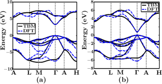
The HSE-DFT band structure serves as the reference for the TB fitting procedure, for which we use a least-square fitting at the point and points along the and directions, following the guidelines given in Ref. vogl_1983, . This ensures that the energetic positions near the CB and VB edges as well as the curvature of the different TB bands in the vicinity of the point are in good agreement with the HSE-DFT calculations. Furthermore, using the guidelines of Ref. vogl_1983, , chemical trends are also taken into account. The resulting TB band structures in comparison with the HSE-DFT band structure for InN and GaN are shown in Fig. 8.
However, as discussed above, and for example in more detail in Ref. moses_2011, , even HSE-DFT calculations underestimate the bulk band gap. Since this quantity is of central importance for a detailed comparison with experimental data, we adjust our TB model to reproduce the experimental band gap. In order to do so, here we shift the on-site cation -orbital energies. This procedure affects mainly the CB edge and bands energetically further away from the VB and CB edges. These bands are of secondary importance for the description of the band gap bowing in InGaN alloys. Table 2 summarizes the resulting TB parameters.
| InN | GaN | |
|---|---|---|
| -11.92 | -10.62 | |
| 0.49 | 0.82 | |
| 0.46 | 0.79 | |
| 0.48 | 0.91 | |
| 6.53 | 6.68 | |
| -1.61 | -5.97 | |
| 1.79 | 2.34 | |
| 4.83 | 5.47 | |
| 1.89 | 4.09 | |
| 6.14 | 8.67 |
V.2 Tight-binding description for alloys
In the framework of a TB model, the InGaN alloy is modeled on an atomistic level. The TB parameters at each atomic site of the underlying wurtzite lattice are first set according to the bulk values of the respective occupying atoms. While for the cation sites (Ga, In) the nearest neighbors are always nitrogen atoms and there is no ambiguity in assigning the TB on-site and nearest neighbor matrix elements, this classification is more difficult for the nitrogen atoms. In this case the nearest-neighbor environment is a combination of In and Ga atoms. Here, we apply the widely used approach of using weighted averages for the on-site energies according to the number of neighboring In and Ga atoms. oreilly_2002 ; li_1992 ; boykin_2007 The hopping matrix elements are chosen according to the values for InN or GaN.
In setting up the Hamiltonian, one must also include the local strain and the total built-in potential to ensure an accurate description of the electronic properties of the InGaN alloy. Several authors have shown that this can be done by introducing on-site corrections to the TB matrix elements , jancu_1998 ; boykin_2002 where and denote lattice sites and and are the orbital types. Therefore, we proceed in the following way. The strain dependence of the TB matrix elements is included via the Pikus-Bir Hamiltonian winkelnkemper_2006 ; schulz_2010_b as a site-diagonal correction:
| (32) |
with
| (33) |
where the denote the VB deformation potentials, while and are the CB deformation potentials. 444Note that the quantities and given by Vurgaftman and Meyer in their 2003 review article vurgaftman_2003 are not the CB deformation potentials and , respectively. The quantities denoted by and in Ref. vurgaftman_2003, are the band gap deformation potentials, e.g. and . With this approach, the relevant deformation potentials for the highest VB and lowest CB states are included directly without any fitting procedure. In the work described below, the deformation potentials for InN and GaN are taken from HSE-DFT calculations. yan_2009 Again, on the same footing as in the case of the on-site energies for the nitrogen atoms, we use weighted averages to obtain the strain-dependent on-site corrections for InxGa1-xN. Our approach is similar to that used for the strain dependence in an 8-band kp model, winkelnkemper_2006 but has the benefit that the TB Hamiltonian still takes the correct symmetry of the system into account, and is sensitive to In, Ga and N atoms.
To obtain the local strain tensor at each lattice site, we perform in a first step a relaxation of the atomic positions in N supercells based on the VFF outlined in Section IV. From the relaxed atomic positions, we calculate according to the method in Ref. pryor_1998, via: 555Note that the definition of the strain matrix done by Pryor et al. pryor_1998 is related to ours via a transposition operation.
| (40) | ||||
| (44) |
where , and are the distorted tetrahedron edges, while , and are the ideal tetrahedron edges. is the identity matrix. The built-in potential is likewise included as a site-diagonal contribution in the TB Hamiltonian. This is also a widely used approach. ranjan_2003 ; saito_2002 ; schuh_2012
VI Results
In the following we use our TB model, including local strain and built-in potentials to analyze the band gap bowing of InGaN. We outline the procedure for TB supercell calculations in Section VI.1, while in Section VI.2 we compare our theoretical results for transition energies and band gap bowing parameters against experimental and other theoretical data. The impact of local alloy composition, local strain and local built-in potential on the CB and VB edges of InGaN alloys is discussed in Section VI.3.
VI.1 TB supercell calculations for InGaN
In the following, all calculations are performed on supercells containing approximately 12,000 atoms, with periodic boundary conditions applied. A large number of atoms are included in the supercell to suppress the influence of finite-size supercell effects. We assume that InGaN is a random alloy, following recent experimental indication. galtrey_2007 ; humphreys_2007 For each In concentration we have performed calculations with five different microscopic configurations, where the In atoms are placed randomly in the supercell. We calculate the band gap as a configurational average, i.e.
| (45) |
where denotes the microscopic configuration and () is the corresponding CB (VB) edge. The number of configurations is given by .
VI.2 Band gap bowing in InGaN: Comparison with experiment
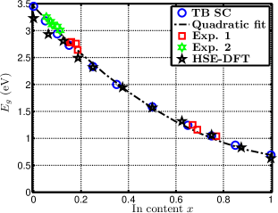
Figure 9 shows TB supercell calculation results (open blue circles) for the band gap of InxGa1-xN as a function of the In content . The TB results are compared to recent experimental data mccluskey_2003 ; schley_2007 ; sakalauskas_2012 and HSE-DFT calculations moses_2011 . From Fig. 9 one can infer that our TB results are in excellent agreement with the HSE-DFT results for In contents above 15%–20% (). For values below 15% the fact that the HSE-DFT calculations underestimate the band gap of GaN becomes important. However, in this composition regime (), our TB results are in very good agreement with the experimental data, cf. Fig. 9. Also in the high In content regime () the TB data is in very good agreement with the experimental data. text: We have applied this model to AlInN too, also showing an excellent agreement with recent experimental data. schulz_2013
For the design of InxGa1-xN based optoelectronic devices, knowledge about the behavior of the band gap with composition is of central importance. Usually the dependence of on is described by a quadratic function in , involving the energy gaps of InN (), GaN () and a bowing parameter :
| (46) |
Commonly, the band gap bowing parameter of InGaN is assumed to be composition independent. vurgaftman_2003 We start with this assumption and denote the composition independent bowing parameter by . In doing so we find a bowing parameter eV. Experimentally determined bowing parameters scatter quite significantly, ranging from 1.43 eV to 2.8 eV. Theoretical values for range from 1.36 to 5.14 eV. Compared to both theory and experiment our reported value of eV is therefore within the range of the reported literature values. However, it has been suggested wetzel_1998 ; mccluskey_1998 that the bowing parameter of N alloys is composition dependent. Based on HSE-DFT calculations for special quasirandom structures (SQSs), Moses et al. moses_2011 found that ranges in InxGa1-xN from 2.29 eV () to 1.14 eV (). Gorczyca et al. gorczyca_2009 used LDA+C calculations to analyze in InxGa1-xN alloys. The authors considered two types of alloys, i.e. i) alloys with uniformly distributed In atoms in a 32-atom supercell and ii) alloys with all In atoms clustered. In case i) Gorczyca et al. gorczyca_2009 reported that ranges from 1.7 eV (large ) to 2.8 eV (small ). For the authors found for the uniform case eV. Looking at case ii), the clustered alloy, band gap bowing values between 2.5 eV (large ) and 6.5 eV have been reported, with eV. Based on our random TB supercell calculations, we find that our bowing parameter shows a strong composition dependence. The TB results for are summarized in Table 3. Here, the values for range from 1.78 eV (large ) to 2.77 eV (small ). At we find eV. Therefore, our results are close to the results obtained from the LDA+C calculations in the case of an uniform alloy (see above).
To shed more light on the composition dependence of , we investigate in a second step how the CB and VB edge behave as a function of the In content . These quantities are also of great interest for the design of InGaN/GaN based optoelectronic devices, since the CB and VB edge energies in InGaN affect the confinement energies of electron and hole wave functions. Here, to calculate the bowing parameters and for the CB and VB edge, respectively, we use:
| (47) |
where and are the CB and VB edges, respectively. These quantities are obtained from our TB SC calculations. The VB offset is denoted by and taken from HSE-DFT data in Ref. moses_2011, . Here, and are composition-dependent fitting parameters to reproduce and , respectively. The resulting composition-dependent values for and are summarized in Table 3. From this table one infers that, while is almost composition independent, varies significantly with . Consequently, the composition dependence of the band gap bowing arises mainly from the composition dependence of the CB edge. This result is in agreement with the HSE-DFT findings of Ref. moses_2011, . Therefore, when modeling InGaN based heterostructures in the framework of a continuum description, such as kp theory, the composition dependent bowing of the band edges should be taken into account in order to achieve a realistic description of these systems.
To extend the analysis of the band edges in InGaN alloys further we focus in the next section on the impact of local composition, local strain and local built-in potentials on the CB and VB edge, respectively.
| 5% | 10% | 15% | 25% | 35% | 50% | 65% | 75% | 85% | |
|---|---|---|---|---|---|---|---|---|---|
| (eV) | 2.77 | 2.6 | 2.42 | 2.28 | 2.13 | 1.94 | 1.82 | 1.78 | 1.82 |
| (eV) | 1.74 | 1.56 | 1.43 | 1.26 | 1.13 | 0.92 | 0.85 | 0.81 | 0.78 |
| (eV) | -1.03 | -1.04 | -0.99 | -1.02 | -1.00 | -1.02 | -0.97 | -0.97 | -1.04 |
VI.3 Impact of local composition, strain and built-in potential on CB and VB edges in InGaN
In the previous section we have discussed the composition dependence of the bowing parameters and of the CB and VB edges, respectively. These calculations included local strain and built-in potential effects due to alloy fluctuations. Here we analyze in more detail how the different contributions from pure alloy fluctuations, local strain and built-in potential effects influence the CB and VB edge energies. Figure 10 shows the CB (left) and VB (right) edge energies as a function of the In content .
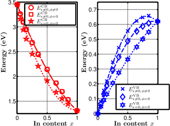
In a first step, to study the impact of the alloy fluctuations only, we neglect the local strain and built-in field effects in the TB SC calculations of the band edges (, ). As Fig. 10 shows, in the absence of strain and built-in potential, varies almost linearly with the In content , while shows a strong non-linear behavior. Using Eqs. (47), we can determine and for the case of . The results for the composition-independent bowing parameters and are summarized in Table 4. When including local strain effects but neglecting the local built-in potential, is shifted to higher energies over the whole composition range due to hydrostatic strain in the system, (cf. Fig. 10). This reduces the CB edge bowing parameter by a factor of two compared to the situation without strain and built-in potential effects (cf. Table 4). When looking at the behavior of in comparison to we find also a shift to higher energies resulting from biaxial compressive strain. However, in this case the magnitude of the VB edge bowing parameter is increased by a factor of three compared to the situation without strain and built-in potential (cf. Table 4). When including both local strain and built-in potential effects, in comparison to is almost unaffected. This is also reflected in the data for the CB edge bowing parameter shown in Table 4. For the VB edge this is not the case. Here, the local built-in potential significantly modifies the VB edge, as seen in Fig. 10. Moreover, due to local built-in potential effects, exceeds the InN/GaN VB offset . The consequence of this behavior would be that InxGa1-xN on InN would be a type-II heterostructure for .
| (eV) | (eV) | (eV) | |
|---|---|---|---|
| 2.24 | 2.01 | -0.23 | |
| 1.70 | 1.01 | -0.69 | |
| 2.02 | 1.03 | -0.99 |
This difference in the behavior of the CB and VB edges can be attributed in part to the differences in the effective masses. Compared to the VB, the effective mass of the CB edge is small. rinke_2008 ; schulz_2010_b Therefore, in the regime of large (high In content), the randomly distributed In atoms can form QD-like regions that lead to a localization of VB wave functions since the local compressive strain favors this behavior. schulz_2012c Therefore, we observe a strong increase in the magnitude of when including strain effects, cf. Fig. 10 and Table 4. In contrast, the compressive hydrostatic strain in these regions leads to a weaker localization of the CB wave functions and a shift to higher energies, schulz_2012c as observed in Fig. 10. However, since the CB wave functions are only weakly localized in the QD-like regions due to strain effects and the low effective masses, the local built-in potential is of secondary importance for the CB edge. However, originating from the much stronger VB wave function localization, as in a “real” nitride-based QD, the built-in potential further increases the localization and leads to a pronounced shift to higher energies. williams_2009 As seen for example in experiments on -plane GaN/AlN QDs, due to the presence of the built-in potential the measured photoluminescence (PL) energy drops below the GaN band gap value. simon_2003
VII Summary
We have presented a complete theory of local electric polarization in the linear piezoelectric limit. The connection between the local polarization and local internal strain is obtained in an elegant manner through the use of Born effective charges and internal strain parameters. We have validated the theory for the highly ionic III-N wurtzite compounds, demonstrating a high degree of agreement between our model and Berry-phase calculations. We have cast these local effects in the form of a local piezoelectric tensor, which helps to highlight the importance of local strain and tetrahedron orientation on the polarization field and potential. In addition to this, we have obtained a consistent series of polarization-related ab initio parameters for the group-III nitrides.
We have also presented a point dipole method for the calculation of the local polarization potential that overcomes resolution problems encountered when solving directly Poisson’s equation. The method involves the discretization of the polarization field as a series of point dipoles. The accuracy of the method has been tested against a well known problem with analytical solution. As an example, we have applied our theory and methodology to study the local polarization and local polarization potential in polar and non-polar InGaN/GaN QW structures, where we have observed large local fluctuations in both quantities.
Finally, we have presented a tight-binding model that allows us to take into account local alloy effects, including local strain and the local polarization potential discussed throughout the paper. With this model we have calculated the composition dependence of the band gap of InGaN and provided composition-dependent bowing parameters for the band gap and both the conduction and valence band edge energies. Furthermore, we have shown that the local polarization potential has a strong influence on wave function localization effects in the valence band of this material.
Acknowledgements.
M. A. C. would like to thank Vincenzo Fiorentini and David Vanderbilt for very useful discussions on the practicalities of Berry-phase calculations. S. S. would like to thank Muhammad Usman for valuable discussions. This work was carried out with the financial support of Science Foundation Ireland under project number 10/IN.1/I2994. S. S. also acknowledges financial support from the European Union Seventh Framework Programme (ALIGHT FP7-280587).Appendix A Example of the calculation of a local piezoelectric coefficient
To illustrate how the calculation of the local piezoelectric tensor in terms of the internal strain parameters is done, we give here the details of the calculation for . The expression of for is simplified to
| (48) |
where we have made use of the Voigt relation . is given by the WZ internal parameter, and for A being a cation. We need to calculate . Looking at Fig. 3, it is clear that the nearest neighbors of A are B, which we label 1, and three periodic replicas of D contained in a plane below A, which we label 2–4. If A is fixed at the origin, , then the distances of the different nearest neighbors from A are given by:
| (49) |
where a, b and c are the (strained) lattice vectors of the unit cell. Since for this example we are interested in only, we set all the strain components to zero except for . Following all the definitions given in Ref. caro_2012c, (with exchanged notation ), we can write:
| (50) |
To obtain we sum over nearest-neighbor distances:
| (51) |
The last term of Eq. (48) therefore reduces to
| (52) |
which leads to the final result:
| (53) |
Appendix B Point dipole method for the calculation of local polarization potentials
Proceeding in a similar manner to the one employed by Jackson for a point charge, jackson_1999 we can obtain the exact analytic solution for the potential due to a point dipole when only one interface is present, as schematically shown in Fig. 11:

| (54) |
with
| (55) |
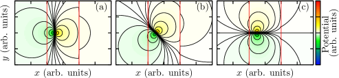
where is the image dipole used, together with the original dipole p, for the calculation of the potential in region (1) and is the image dipole used for the calculation of the potential in region (2). Their positions are given by and , respectively. The results for a test dipole of arbitrary magnitude when one of the materials has a dielectric constant twice as big as that of the material in which the dipole is contained are shown in Fig. 12(a–c) for three different orientations of the dipole.
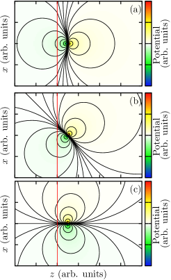
The calculation of the potential when a second interface is included is more complicated, as additional mirror images have to be added to balance the two initial image dipoles about each interface. As a result, an infinite number of reflections (and hence, image dipoles) have to be considered in order to obtain the exact form of the potential. These reflections up to third order are shown in Fig. 13. The treatment for a point charge in such a situation has been already done by Barrera. barrera_1978 For the case of a point dipole, we find the expressions to be similar although the transformation of the point dipole is somehow different compared to the point charge due to the vector nature of the former. Details of our treatment and expressions for the three-media case are given in the next section.
B.1 Point dipole solution for the three-dielectric problem
Building on the description made by Barrera for point charges in a three-dielectric configuration, barrera_1978 we give here the analogous solution for point dipoles. The reflections necessary to construct the image point dipoles are illustrated in Fig. 13.
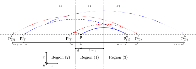
Following the convention of Fig. 13, where is the distance from the dipole to the left side interface and is the distance between the two interfaces, we can obtain a set of rules for the form of the image charges and , being the reflections of p starting at left and right, respectively. These rules can be written as the following expressions. For the position of the image dipoles:
| (56) |
and for the value of the image dipoles:
| (57) |
for the first series and
| (58) |
for the second series, with .
Finally the expression of the potential in all three regions can be written as
| (59) |
It is implicit in Eq. (59) that for the calculation of the potential in region (2) only the image dipoles in region (3) (together with the original dipole) are taken into account, and vice-versa. Given the form of Eq. (59) it is clear that an exact solution to the problem of three media cannot be obtained for a finite number of terms in the summation. However, approximate solutions can be obtained whose accuracy will depend mostly on the difference in the values of the dielectric constants of the different materials. In Fig. 14 we show approximations up to third order reflections, for different orientations of the dipole, in the case of three materials for which and . This is an extreme case in the context of III-V compounds, for which the differences in between materials do not usually go beyond 50%. For clarity of interpretation, the potential isolines shown decay as a power of 2, which allows to visualize the fine effects of the interfaces far from the dipole. As can be seen, the second order correction [Figs. 14(d–f)] is already very well converged for this extreme case and we expect first order corrections to be sufficient for the materials of interest, group-III nitrides in particular.
B.2 Gaussian smearing of point dipoles
As mentioned in the paper, the potential solution for a point dipole is an approximation to the potential due to the dipole moment of a charge distribution. jackson_1999 This approximation is only valid in the limit when the potential is calculated sufficiently far away from the charge distribution. How far is “sufficiently far” depends on the particular problem at hand, basically on the value of the dipole and the volume over which the charge density giving rise to the dipole moment spread originally. A Gaussian smearing of the dipoles that are close to the position where the potential is calculated, is a straightforward manner to deal with this problem, as the parameters controlling the smearing can be tuned easily at need. We propose the implementation of this smearing controlled by two parameters:
-
1.
is the cut-off radius for which all the dipoles that obey are smeared, where r is the position where the potential is calculated and is the position of the dipole under consideration.
-
2.
is the standard deviation of the Gaussian function that produces the smearing. It gives a measure of the volume over which the dipole is smeared.
Therefore, the expression for the potential at r due to a dipole p located at can be rewritten, in spherical coordinates, as
| (60) |
where is given by
| (61) |
Typically, the integration in can be done up to a certain cutoff since the value of the integrand will decay rapidly. For example, our current implementation sets as the upper limit for the integration, which comprises a volume that contains about 99% of the total original dipole moment p. The extension of Eq. (60) to the case in which different dielectric constants are present is straightforward and done in the same way as explained in the paper and Section B.1 of this Appendix.
B.3 Computational aspects: method of layers and application to quantum wells
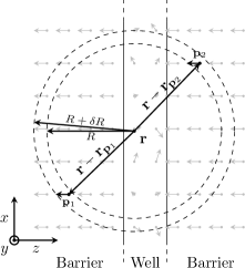
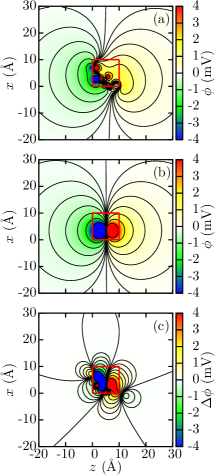
It is clear that when dealing with real size structures, for which the polarization is sampled at a very elevated number of sites, the calculation of the potential becomes very expensive. In particular, for each r, a summation over all the dipoles present in the system has to be carried out:
| (62) |
In a system where the density of dipoles is approximately constant, for instance one dipole located at each cation site in Ref. caro_2012, , the number of dipoles contributing to Eq. (62) located at distances between and from r is proportional to the surface area of a sphere of radius :
| (63) |
where is an infinitesimal increment in . Because the contribution to from each dipole decreases like , as given by Eq. (26), Eq. (63) implies that the contribution to due to the dipoles located at for which is of the same order of magnitude as the contribution due to dipoles for which , for any arbitrary . In other words, in principle, the sum in Eq. (62) does not converge. In practice, for real structures such as InGaN/GaN QWs, the fact that there is a dot product involved in the calculation of the potential due to each dipole, and also that the dipoles in the barrier typically point in the same direction, give rise to opposite contributions that tend to cancel each other as increases, as schematically shown in Fig. 15. In that case, the sum does converge although rather slowly. We have implemented two different methods to speed up the convergence of the sum in Eq. (62), one of which can be applied to any system, the “method of layers”. The other method can be applied to systems where some assumption can be made about the value of the polarization being constant in the greatest part of the system, as is the case in QWs. An outline of these methods is given next.
B.3.1 Method of layers
In the same way that a point dipole is an approximation for a charge density distribution valid far away from the location of the dipole, it can be shown that a point dipole can be a valid approximation for a given ensemble of neighbouring point dipoles at a certain distance from the ensemble. Figure 16(a) shows the potential due to an ensemble of dipoles , of typical magnitude in nitride QWs, that are localized in a restricted region in space, each at position . This ensemble can be approximated by a single dipole P whose magnitude equals the summation of all the original dipoles and whose position is given by the weighted average of the dipoles in the ensemble [Fig. 16(b)]:
| (64) |
As shown in Fig. 16(c), the difference between an ensemble of dipoles and its correspondent approximation calculated as in Eq. (64) decays rapidly away from the ensemble. Applying Eq. (64) recurrently, one can construct, around the point r where the potential is being calculated, a system of “layers” in which the density of dipoles decreases as one moves away from r.
B.3.2 Simplification for quantum wells
A simplification can be made for QW systems, or even a quantum dot (QD) system, if a constant value for the polarization can be assumed for the greatest part of the system. Since only differences in polarization are meaningful for the calculation of polarization potentials, an arbitrary constant shift of the polarization of the whole system will not have any effect on the calculated value of the polarization potential. This shift can be chosen in such a way that the resultant polarization, at least on average, is zero in the barrier in the case of a QW, or in the unstrained barrier in the case of a QD. 666The strain field will not vanish in the barrier material immediately around a QD, but will effectively be zero far away from it. See for instance Ref. pryor_1998, . In that case, all the dipoles arising from that region, once the discretization described in the paper is made, will have value zero. Therefore, the dipoles contained within that region can be left out of the calculation.
References
- (1) O. Ambacher, J. Majewski, C. Miskys, A. Link, M. Hermann, M. Eickhoff, M. Stutzmann, F. Bernardini, V. Fiorentini, V. Tilak, B. Schaff, and L. F. Eastman, J. Phys.: Condens. Matter 14, 3399 (2002)
- (2) G. Bester, X. Wu, D. Vanderbilt, and A. Zunger, Phys. Rev. Lett. 96, 187602 (2006)
- (3) A. Beya-Wakata, P.-Y. Prodhomme, and G. Bester, Phys. Rev. B 84, 195207 (2011)
- (4) M. A. Caro, S. Schulz, and E. P. O’Reilly, Phys. Stat. Sol. B 249, 526 (2012), http://dx.doi.org/10.1002/pssb.201100402
- (5) M. Grundmann, O. Stier, and D. Bimberg, Phys. Rev. B 52, 11969 (1995)
- (6) S. Schulz, M. A. Caro, E. P. O’Reilly, and O. Marquardt, Phys. Rev. B 84, 125312 (2011)
- (7) T. Takeuchi, S. Sota, M. Katsuragawa, M. Komori, H. Takeuchi, H. Amano, and I. Akasaki, Jpn. J. Appl. Phys. 36, L382 (1997)
- (8) M.-H. Kim, M. F. Schubert, Q. Dai, J. K. Kim, E. F. Schubert, J. Piprek, and Y. Park, Appl. Phys. Lett. 91, 183507 (2007)
- (9) W. Lee, M.-H. Kim, D. Zhu, A. N. Noemaun, J. K. Kim, and E. F. Schubert, J. Appl. Phys. 107, 063102 (2010)
- (10) M. A. Caro, S. Schulz, S. B. Healy, and E. P. O’Reilly, J. Appl. Phys. 109, 084110 (2011)
- (11) S. Schulz and E. P. O’Reilly, Phys. Rev. B 82, 033411 (2010)
- (12) D. P. Williams, S. Schulz, A. D. Andreev, and E. P. O’Reilly, IEEE J. Sel. Top. Quantum Electron. 15, 1092 (2009)
- (13) J. P. Perdew and M. Levy, Phys. Rev. Lett. 51, 1884 (1983)
- (14) A. Seidl, A. Görling, P. Vogl, J. A. Majewski, and M. Levy, Phys. Rev. B 53, 3764 (1996)
- (15) G. Klimeck, S. S. Ahmed, H. Bae, N. Kharche, S. Clark, B. Haley, S. Lee, M. Naumov, H. Ryu, F. Saied, M. Prada, M. Korkusinski, T. B. Boykin, and R. Rahman, IEEE Trans. Electron. Dev. 54, 2079 (2007)
- (16) G. Klimeck, S. S. Ahmed, N. Kharche, M. Korkusinski, M. Usman, M. Prada, and T. B. Boykin, IEEE Trans. Electron. Dev. 54, 2090 (2007)
- (17) J. F. Nye, Physical properties of crystals: their representation by tensors and matrices (Oxford University Press, Oxford, 1985)
- (18) H. Grimmer, Acta Crystallogr. Sect. A: Foundations of Crystallography 63, 441 (2007)
- (19) One can also define a second-order piezoelectric tensor to characterize piezoelectricity further away from equilibrium. See Ref. \rev@citealpnumgrimmer_2007
- (20) Note that in Voigt notation, , , , , and .
- (21) R. Resta and D. Vanderbilt, “Physics of ferroelectrics: a modern perspective,” (Springer-Verlag, Berlin Heidelberg, 2007) Chap. Theory of Polarization: A Modern Approach
- (22) R. D. King-Smith and D. Vanderbilt, Phys. Rev. B 47, 1651 (1993)
- (23) D. Vanderbilt and R. D. King-Smith, Phys. Rev. B 48, 4442 (1993)
- (24) R. Resta, Ferroelectrics 136, 51 (1992)
- (25) R. Resta, Rev. Mod. Phys. 66, 899 (1994)
- (26) F. Bernardini, V. Fiorentini, and D. Vanderbilt, Phys. Rev. B 56, 10024 (1997)
- (27) M. A. Caro, S. Schulz, and E. P. O’Reilly, J. Phys.: Condens. Matter 25, 025803 (2013)
- (28) X. Gonze and C. Lee, Phys. Rev. B 55, 10355 (1997)
- (29) M. A. Caro, S. Schulz, and E. P. O’Reilly, Phys. Rev. B 86, 014117 (2012)
- (30) F. Bernardini and V. Fiorentini, Phys. Rev. B 64, 085207 (2001)
- (31) J. Pal, G. Tse, V. Haxha, M. Migliorato, and S. Tomić, Phys. Rev. B 84, 085211 (2011)
- (32) V. Fiorentini, F. Bernardini, and O. Ambacher, Appl. Phys. Lett. 80, 1204 (2002)
- (33) P.-Y. Prodhomme, A. Beya-Wakata, and G. Bester, Phys. Rev. B 88, 121304 (2013)
- (34) S. Nakamura, S. J. Pearton, and G. Fasol, The blue laser diode: the complete story (Springer-Verlag, Berlin Heidelberg, 2000)
- (35) M. R. Krames, O. B. Shchekin, R. Mueller-Mach, G. O. Mueller, L. Zhou, G. Harbers, and M. G. Craford, J. Disp. Technol. 3, 160 (2007)
- (36) U. K. Mishra, S. Likun, T. E. Kazior, and Y. F. Wu, P. IEEE 96, 2875 (2008)
- (37) J. Wu, J. Appl. Phys. 106, 011101 (2009)
- (38) T. Aschenbrenner, H. Dartsch, C. Kruse, M. Anastasescu, M. Stoica, M. Gartner, A. Pretorius, A. Rosenauer, T. Wagner, and D. Hommel, J. Appl. Phys. 108, 063533 (2010)
- (39) Vienna Ab initio Simulation Package (vasp), [http://www.vasp.at], see also on line documentation
- (40) G. Kresse and J. Furthmüller, Phys. Rev. B 54, 11169 (1996)
- (41) P. E. Blöchl, Phys. Rev. B 50, 17953 (1994)
- (42) G. Kresse and D. Joubert, Phys. Rev. B 59, 1758 (1999)
- (43) J. Heyd, G. E. Scuseria, and M. Ernzerhof, J. Chem. Phys. 118, 8207 (2003)
- (44) J. Heyd and G. E. Scuseria, J. Chem. Phys. 121, 1187 (2004)
- (45) J. P. Perdew and A. Zunger, Phys. Rev. B 23, 5048 (1981)
- (46) T. M. Henderson, J. Paier, and G. E. Scuseria, Phys. Stat. Sol. B 248, 767 (2011)
- (47) Q. Yan, P. Rinke, M. Scheffler, and C. G. Van de Walle, Appl. Phys. Lett. 95, 121111 (2009)
- (48) A. Zoroddu, F. Bernardini, P. Ruggerone, and V. Fiorentini, Phys. Rev. B 64, 045208 (2001)
- (49) Private communication with V. Fiorentini and D. Vanderbilt.
- (50) S. Muensit, E. M. Goldys, and I. L. Guy, Appl. Phys. Lett. 75, 3965 (1999)
- (51) F. Bernardini and V. Fiorentini, Appl. Phys. Lett. 80, 4145 (2002)
- (52) I. Vurgaftman and J. R. Meyer, J. Appl. Phys. 94, 3675 (2003)
- (53) S. Schulz, A. Berube, and E. P. O’Reilly, Phys. Rev. B 79, 081401(R) (2009)
- (54) S. Schulz, M. A. Caro, E. P. O’Reilly, and O. Marquardt, Phys. Stat. Sol. B 249, 521 (2012)
- (55) K. Shimada, Jpn. J. Appl. Phys. 45, L358 (2006)
- (56) S.-H. Wei, L. G. Ferreira, J. E. Bernard, and A. Zunger, Phys. Rev. B 42, 9622 (1990)
- (57) F. Bernardini and V. Fiorentini, phys. stat. sol. (a) 190, 65 (2002)
- (58) G. Bester and A. Zunger, Phys. Rev. B 71, 045318 (2005)
- (59) J. D. Jackson, Classical Electrodynamics, 3rd ed. (John Wiley & Sons, New York, 1999)
- (60) T. Paskova, phys. stat. sol. (b) 245, 1011 (2008)
- (61) P. N. Keating, Phys. Rev. 145, 637 (1966)
- (62) C. Pryor, J. Kim, L. W. Wang, A. J. Williamson, and A. Zunger, J. Appl. Phys. 83, 2546 (1998)
- (63) D. Camacho and Y. M. Niquet, Physica E 42, 1361 (2010)
- (64) R. M. Martin, Phys. Rev. B 6, 4546 (1972)
- (65) P. G. Moses, M. Miao, Q. Yan, and C. G. Van de Walle, J. Chem. Phys. 134, 084703 (2011)
- (66) J. A. Chan, J. Z. Liu, and A. Zunger, Phys. Rev. B 82, 045112 (2010)
- (67) E. P. O’Reilly, A. Lindsay, P. J. Klar, A. Polimeni, and M. Capizzi, Semicond. Sci. Technol. 24, 033001 (2009)
- (68) S. Schulz, S. Schumacher, and G. Czycholl, Eur. Phys. J. B 64, 51 (2008)
- (69) Q. Yan, P. Rinke, M. Scheffler, and C. G. Van de Walle, Appl. Phys. Lett. 97, 181102 (2010)
- (70) A. Kobayashi, O. F. Sankey, S. M. Volz, and J. D. Dow, Phys. Rev. B 28, 935 (1983)
- (71) M. Murayama and T. Nakayama, Phys. Rev. B 49, 4710 (1994)
- (72) K. Leung, S. Pokrant, and K. B. Whaley, Phys. Rev. B 57, 12291 (1998)
- (73) M. A. Caro, S. Schulz, and E. P. O’Reilly, Phys. Rev. B 86, 099901(E) (2012)
- (74) P. Vogl, H. P. Hjalmarson, and J. D. Dow, J. Phys. Chem. Solids 44, 365 (1983)
- (75) E. P. O’Reilly, A. Lindsay, S. Tomić, and M. Kamal-Saadi, Semicond. Sci. Technol. 17, 870 (2002)
- (76) Z. Q. Li and W. Pötz, Phys. Rev. B 46, 2109 (1992)
- (77) T. B. Boykin, N. Kharche, G. Klimeck, and M. Korkusinski, J. Phys.: Condens. Matter 19, 036203 (2007)
- (78) J.-M. Jancu, R. Scholz, F. Beltram, and F. Bassani, Phys. Rev. B 57, 6493 (1998)
- (79) T. Boykin, G. Klimeck, R. C. Bowen, and F. Oyafuso, Phys. Rev. B 66, 125207 (2002)
- (80) M. Winkelnkemper, A. Schliwa, and D. Bimberg, Phys. Rev. B 74, 155322 (2006)
- (81) S. Schulz, T. J. Badcock, M. A. Moram, P. Dawson, M. J. Kappers, C. J. Humphreys, and E. P. O’Reilly, Phys. Rev. B 82, 125318 (2010)
- (82) Note that the quantities and given by Vurgaftman and Meyer in their 2003 review article vurgaftman_2003 are not the CB deformation potentials and , respectively. The quantities denoted by and in Ref. \rev@citealpnumvurgaftman_2003 are the band gap deformation potentials, e.g. and .
- (83) Note that the definition of the strain matrix done by Pryor et al. pryor_1998 is related to ours via a transposition operation.
- (84) V. Ranjan, L. Bellaiche, and E. J. Walter, Phys. Rev. Lett. 90, 257602 (2003)
- (85) T. Saito and Y. Arakawa, Physica E 15, 169 (2002)
- (86) K. Schuh, S. Barthel, O. Marquardt, T. Hickel, J. Neugebauer, G. Czycholl, and F. Jahnke, Appl. Phys. Lett. 100, 092103 (2012)
- (87) M. J. Galtrey, R. A. Oliver, M. J. Kappers, C. J. Humphreys, D. J. Stokes, P. H. Clifton, and A. Cerezo, Appl. Phys. Lett. 90, 061903 (2007)
- (88) C. J. Humphreys, Philos. Mag. 87, 1971 (2007)
- (89) M. D. McCluskey, C. G. Van de Walle, L. T. Romano, B. S. Krusor, and N. M. Johnson, J. Appl. Phys. 93, 4340 (2003)
- (90) P. Schley, R. Goldhahn, A. T. Winzer, G. Gobsch, V. Cimalla, O. Ambacher, H. Lu, W. J. Schaff, M. Kurouchi, Y. Nanishi, M. Rakel, C. Cobet, and N. Esser, Phys. Rev. B 75, 205204 (2007)
- (91) E. Sakalauskas, Ö. Tuna, A. Kraus, H. Bremers, U. Rossow, C. Giesen, M. Heuken, A. Hangleiter, G. Gobsch, and R. Goldhahn, Phys. Stat. Sol. B 249, 485 (2012)
- (92) S. Schulz, M. A. Caro, L.-T. Tan, P. J. Parbrook, R. W. Martin, and E. P. O’Reilly, Appl. Phys. Express 6, 121001 (2013).
- (93) C. Wetzel, T. Takeuchi, S. Yamaguchi, H. Katoh, H. Amano, and I. Akasaki, Appl. Phys. Lett. 73, 1994 (1998)
- (94) M. D. McCluskey, C. G. V. de Walle, C. P. Master, L. T. Romano, and N. M. Johnson, Appl. Phys. Lett. 72, 2725 (1998)
- (95) I. Gorczyca, S. P. Łepkowski, T. Suski, N. E. Christensen, and A. Svane, Phys. Rev. B 80, 075202 (2009)
- (96) P. Rinke, M. Winkelnkemper, A. Qteish, D. Bimberg, J. Neugebauer, and M. Scheffler, Phys. Rev. B 77, 075202 (2008)
- (97) S. Schulz and E. P. O’Reilly, Phys. Stat. Sol. B249, 516 (2012)
- (98) J. Simon, N. T. Pelekanos, C. Adelmann, E. Martinez-Guerrero, R. André, B. Daudin, L. S. Dang, and H. Mariette, Phys. Rev. B 68, 035312 (2003)
- (99) R. G. Barrera, O. Guzman, and B. Balaguer, Am. J. Phys 46, 11 (1978)
- (100) The strain field will not vanish in the barrier material immediately around a QD, but will effectively be zero far away from it. See for instance Ref. pryor_1998, .