Large band offset as driving force of 2-dimensional electron confinement: the case of SrTiO3/SrZrO3 interface
Abstract
Using advanced first-principles calculations we predict that the non-polar SrTiO3/SrZrO3 (001) interface, designed as either thin SrZrO3 film deposited on SrTiO3 or short-period (SrTiO3)m/(SrZrO3)n superlattice, host a 2-dimensionally confined electron gas. Mobile electron charge due to native impurities, field-effect, or modulation doping remains tightly trapped at the interface. Key ingredients for this occurrence are a) the peculiar chemistry of 3d orbitals, b) the large band offset at titanate-zirconate interface.
pacs:
73.20.-r, 71.15.-m, 72.15.RnI Introduction
The observations of a 2-dimensional electron gas (2DEG) in SrTiO3/LaAlO3 (STO/LAO) interfaces and superlatticesohtomo ; thiel ; huijben ; reyren ; nakagawa ; herranz triggered a gold rush toward the discovery and design of similar oxide heterostructures that would open the way to a new all-oxide nanoelectronics. Despite extensive efforts, however, 2DEGs in oxide heterostructures remain rare, and a consensus about genuine 2DEG formation emerged only for a handful of systems other than STO/LAO. Among single interfaces we can mention the n-type STO/LaVO3hotta , STO/LaGaO3perna , STO/GaTiO3son ; moe ; cain ; boucherit , and some amorphous STO, LAO, and Al2O3 overlayers grown on STOchen ; lee . Interestingly, a 2DEG was also revealed at the (001) surface of STO thin-filmssyro and at the (001) surface of KTaO3king ; syro1 . An alternative route to the spontaneous 2DEG formation is based on the explicit inclusion of doping layers, e.g. single Nb-doped TiO2 layers introduced in epitaxial STO films in form of a superlattice (SL)ohta_nm ; mune ; ohta_tsf , and single RO layers (with R=La, Pr, Nd, Sm) substitutional to SrO in STOjang .
From the conceptual perspective, years of studies were not yet sufficient to reach, from this variety of observations, a common understanding on the essential ingredients causing the 2DEG formation in oxide heterostructures. The polar character of the overlayer, the correlated nature of Ti 3d electronic states, the large band-offset at the interface, the dielectric properties of the STO substrate are all generically invoked as 2DEG driving forces, but without a clear definition of what is really essential and what it is not. In particular, one of the most debated aspects concerns the role of film polarity and the related polarization catastrophe. The recent observation of 2DEG at the non-polar (110) STO/LAO interfaceherranz suggests that polarity is in fact not so essential to the 2DEG presence. Theory and simulation, especially based on ab-initio methods, can give an invaluable contributions to this conceptual analysis, not only for their typical accuracy, but also for the capability to enlighten the instrinsic behaviour of the ideal systems (i.e. filtered by the complicacies introduced by disorder, inhomogeneities, structural imperfections, etc.).
Following this line of thought, in this work we furnish a sound proof of concept concerning the presence of 2DEG in an ideal (disorder and defect-free) non-polar oxide heterostructures in form of both single interface and superlattice. Specifically, we predict that a 2DEG system tightly confined to a few atomic layers occurs at the (001) interface between SrTiO3 (STO) and SrZrO3 (SZO)shafranek ; kajdos . Unlike STO/LAO, neither side of the STO/SZO interface is polar, hence no polarization catastrophe can occur and the system is intrinsically insulating. Nevertheless, we will see that the same charge confinement mechanism described for the Ti 3d conduction states in STO/LAOdelugas applies here as well, and a 2DEG of few nm extension shows up at the interface.
In absence of polarization catastrophe, mobile charge must be furnished either by field effect or native defects, or by explicit doping of the SZO side (modulation doping). Field-effect is a very efficient way to manipulate the amount of carriers confined at the interface of oxide heterostructures. As such, it is not only powerful mechanism for current-switching applications but also a convenient and clean way to explore the phase diagram of these systems, as demonstrated by recent reports of field-effect modulated 2DEG superconductivity in STO/LAOreyren ; caviglia , STOueno , and KTaO3ueno1 ; yoshi . Concering chemical doping, we will explore STO/SZO superattices with Zr-Nb and Sr-La substitutions in a single ZrO2 and SrO layer, respectively, thus mimicking the heterostructures realized in Refs.ohta_nm, and jang, . We will see that chemical doping further reduces the extension of 2DEG, which thus become ultra-confined in about 1 nm at the STO/SZO interface. Nicely, our predictions are confirmed by recent experimentskajdos published right after the completion of this work, revealing the presence of a 2DEG in STO/Sr(Ti1-xZrx)O3 heterostructures.
Our results support the viewpoint that the polar catastrophe in STO/LAO, while functional to the charge transfer from surface to interface, is not instrumental to the confimenent process in itself. In fact, essential ingredients for the electron charge confinement are the chemistry of 3d Ti orbitals, the large misalignment between STO and SZO conduction bands, and the electric field due to the electrostatic potential offset at the interface.
II Method
The accurate ab-initio description of oxide heterostructures requires an advanced computational method capable of reproducing the band gap of the individual components as well as their band alignment at the interface, both of which are generally outside the capability of standard local-density functional (LDA) methods. Here we use the pseudo-self interaction correction approach (VPSIC)vpsic , successfully applied to study a number of magnetic and non-magnetic materialsarcher and a series of oxide heterostructures, including the STO/LAO interfacedelugas ; filippetti , Nb:STOdelugas1 and LNO/LAOpuggioni superlattices. This method is an empowered variant of the formerly known pSIC approachpsic ; psic1 , successfully applied to a vast range of strong-correlated systems, including manganitesmanganiti , cupratescuprati , high-K materialshigh-k , and diluted magnetic semiconductorsdms . The VPSIC approach used in this work is implemented in the PWSIC code working on plane-waves plus ultrasoft pseudopotentialuspp basis set. For these calculations we used well-converged cut-off energies (35 Ryd) and dense k-point grids for the Brillouin-zone integration.
For bulk STO and SZO the VPSIC-calculated band gap of 2.9 eV and 5.3 eV (against experimental 3.2 eV and 5.6 eV values) enormously improve the typically 50%-underestimated LDA values; also accurately reproduced are the equilibrium lattice constants calculated for STO (3.915 Å, against experimental 3.905 Å) and SZO (4.13 Å, vs. experimental 4.11 Å). For the simulation of the interfaces we use supercells of 11 and symmetry in the plane, depending on the considered doping concentration, and orthogonal size equal to 13 unit cells (about 50 Å) for single interfaces and up to 17 unit cells (66 Å) for the superlattices.
Charge doping is introduced in two ways. First, for small doping concentrations, we simply add external electron charge with a positive homogeneous charge background restoring neutrality; the electronic structure corresponding to the augmented electron charge is recalculated self-consistently at each doping, thus bypassing the faulty rigid band approximation. This approach mimics a field-effect charge manipulation or charge from native donors of the STO substrate. Second, at large doping concentration we explicitly describe chemical doping by ZrNb and SrLa atomic substitution.
III Results: STO/SZO single interfaces
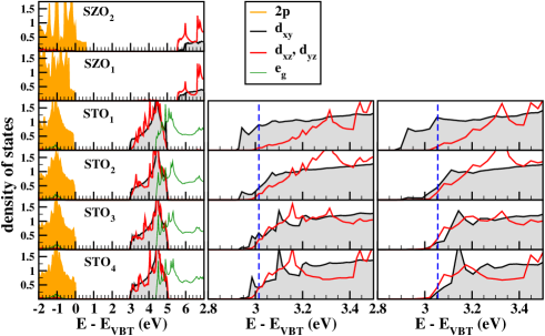
We start considering a (STO)7/(SZO)2/vacuum stoichiometric supercell mimicking a single interface of 2 layers of SZO grown on the STO substrate. Notice that at variance with STO/LAO, this system has only one type of interface, namely TiO2/SrO/ZrO2. The calculated density of states (DOS) decomposed in orbital contributions is reported in Fig.1, left panels. For clarity, only the energy region surrounding the band gap is shown. As expected the system is insulating, with a band gap of about 3 eV in the STO side between O 2p valence bands (VB) and Ti 3d conduction bands (CB). In the surface SZO layer, the band gap is between O 2p and Zr 4d states, and slightly reduced in size (4.9 eV) with respect to its bulk value 5.3 eV due to local structural relaxations. The VB and CB offsets (0.5 eV and 2.5 eV respectively) are substantial, and similar to those obtained in STO/LAO.
Then, exploiting our supercell technique, we introduce excess electron charge, to be interpreted as due to field-effect modulation. We consider two sheet concentrations, n2D=3.3 and 6.6 1013cm-2 (0.05 and 0.1 electrons per interface area, respectively). The corresponding DOS, displayed in the middle and right panels of Fig.1, respectively, clearly show that the additional charge does not spread through the STO substrate, but progressively accumulates mainly in the dxy orbital of the Ti layer closest to the interface (STO1, indicated by the filled gray area in the Figure). The onset of the DOS for this orbital is indeed visibly lower in energy than the (dxz, dyz) DOS sited on the same Ti (STO1, red line). Hereafter we call on-site splitting the difference between dxy and (dxz, dyz) conduction band bottoms (CBB), and inter-site splitting, the difference between CBBs of dxy states sited on different Ti layers (being highly localized in the xy plane, each dxy can be unambiguously associated to a given layer).
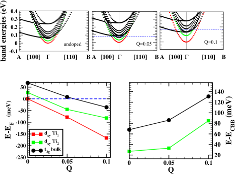
A quantitative analysis of these orbital splittings is given in Fig.2, where band structure and band bottom misalignment at varying doping is reported. Remarkably, both the on-site Ti1 splitting (bottom right panel, black circles) and the inter-site Ti1-T2 splitting (bottom right, green squares) are sizable even for the undoped insulating system (65 meV and 25 meV, respectively), and then they progressively grow with the carrier concentration.
These results indicate that 2D charge confinement in STO/SZO (analogously to STO/LAO) is governed by the size of 3d t2g orbital splitting. The t2g on-site splitting originates from the bi-dimensional and very anisotropic nature of Ti t2g orbitals, which results in very different planar (m∗=0.7 me) and orthogonal (m∗=8.8 me) effective massesdelugas . Since dxz and dyz have lobes oriented orthogonally to the interface, they pay an energy penalty due to the sharp interface potential and shift up in energy with respect to the dxy state – to put it differently, the hopping between adjacent Zr 4d dxz and dyz orbitals is suppressed by the huge (2.5 eV) Zr-Ti CB offset. Clearly the on-site splitting is maximum for Ti1 but it rapidly disappears away from the interface.
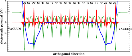
The interpretation of the dxy inter-site splitting is more subtle. We may expect the STO dxy bands to be almost unaffected by the interface and hence remain substantially bulk-like and degenerate. In turn this would leave the charge homogeneously spread through STO. To shed light on this aspect we calculated the averagemacro electrostatic potential along the stacking direction (Fig.3). As expected, the potential is about constant in the STO side, signaling bulk-like behaviour. However, the large electrostatic potential offset ( 2 eV) between the (more repulsive) STO side and the SZO overlayer causes a sharp potential gradient, hence a local electric field 5 107 V/cm acting across the interface region which includes the Ti1 layer. This field causes a 0.1 eV energy lowering of the Ti1 3d states with respect to the bulk-like Ti 3d states of the substrate, and drives the 2D charge confinement. The electrostatic misalignment can be ultimately attributed to the difference between Zr and Ti: both are 4+ ions, but the former is less electronegative (1.33 against 1.54 of Ti in Pauling units), thus it leaves more electrons to the surrounding oxygens. Indeed Fig.3 shows that the planar-averaged total charge (red line) is higher (more positive) in ZrO2 than in TiO2 layers, and correspondingly the electrostatic potential (green line) has deeper attractive wells for ZrO2 than for TiO2.
IV Results: STO/SZO superlattices
Mobile charge can be also introduced at the interface by explicitely doping the SZO layer, e.g. with ZrNb and SrLa substitution. In the following we consider STO10/SZOm superlattices (SLs) (with m up to 7) and doping restricted to a single central SZO layer. These structures are similar in spirit to the Nb-dopedohta_nm ; mune ; delugas1 and La-dopedjang STO SLs where a confined 2DEG forms for appropriate doping and layer thickness. Here we show that the large band offset at the STO/SZO interface strongly enhances the charge confinement present in the doped STO SL, and causes the formation of a very narrow 2DEG.
In Fig.4 orbital-resolved DOS and band energies for the m=3 SL are shown with 50% and 100% ZrNb substitution in the central SZO layer. These two doping concentrations donate 0.25 and 0.5 electrons to each of the two TiO2/SrO/ZrO2 interfaces of the supercell, respectively. According to the band alignment seen for the STO/SZO single interface, we may expect a modulation-doping mechanism which transfers the electron charge from the Nb-doped SZO layer to the undoped STO side. In fact, charge transfer is not complete since Nb5+ is a strongly electronegative ion, thus about 50% of the charge remains trapped in the doped SZO layer, and 25% transferred to each of the two STO sides. We see from the calculated DOS that at both doping concentrations the SL displays a tightly confined 2DEG, with most of the mobile charge trapped in the planar dxy bands of just three layers: the Nb-doped layer (whose CBB lies 1.5 eV and 0.54 eV below EF for 100% and 50% doping, respectively) and the two interface-Ti layers (whose CBB is 0.3 eV below EF for both doping levels). The dxy charges sitting on the Nb-doped layer and the two interface-Ti layers are well separated by the energy barrier due to the undoped SZO layer, whose CBB is placed 1.6 eV above EF. However, we can see a residual tunneling contribution from the orthogonally-extended (dxz, dyz) states across the barrier (red line in the ZrO2 panels of Fig.4). This tunneling can be suppressed by increasing the SZO thickness. To the aim, we performed calculations for thicker SLs up to m=7 (thus with 3 SZO layers between the Nb-doped layer and the STO sides). Tunneling apart, our results indicate that band alignments and charge distribution remain almost unaffected by the increased SZO thickness, thus one SZO layer is already sufficient to induce a fully confined 2DEG.
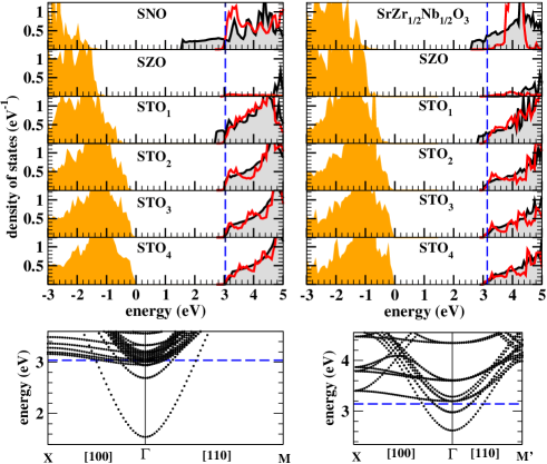
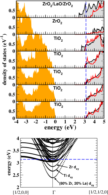
This tight 2DEG confinement has two causes: the presence of the SZO barrier which suppresses the (dxz, dyz) occupancy, and the attractive action of the ionized Nb dopants. Concerning the role of (dxz, dyz) states, it is important to emphasize the difference between this SL and the STO/LAO interface: in the latter a significant portion (about a third) of the 0.5 electrons per unit interface (predicted by the polarization catastrophe) spreads through a multitude of bulk-like (dxz, dyz) bands, thus resulting in a much broader 2DEG (measured thicknessesnakagawa ; basletic ; singh ; dubroka ; copie ; pallecchi indeed reach over 10 nm). In the present case, these states are scarcely populated at 100% doping, and substantially empty at 50% doping, thus the 2DEG has an almost pure dxy character. Nb dopants also excert a remarkable confining action: comparing the DOS profiles in Figs.1 and 4, we can see that the valence band top of the Nb-doped SZO layer is downshifted from +0.6 eV of undoped STO/SZO to -1.6 eV (-0.9 eV) for 100% (50%) doping, thus amplifying the STO/SZO electrostatic potential offset from 2 eV of undoped STO/SZO to 4.2 eV (3.5 eV) for the 100% (50%) doped system.
Results for La-doping are illustrated in Fig.5, where we report DOS and band energy calculations for a STO10/SZO2/LaO/SZO2 SL with a central LaO layer (i.e. 100% Sr-La substitution) sandwiched within two SZO units on both sides. Even in this case a tightly confined 2DEG shows up, with the charge fully confined within five STO layers from the interface. However, La3+ is less electronegative than Nb5+, thus the confinement (i.e. about 2 nm thickness) is slightly looser than for 100% Nb-doping (1 nm). Now, half-electron remains trapped within three monolayers (ZrO2/LaO/ZrO2) of the doped side (only a minor portion in LaO, more than 90% in two adjacent ZrO2), at variance with the 100% Nb-doping case, where half-electron was trapped in just a single NbO2 monoloyer. This slightly broader charge distribution results in a reduced La3+ impurity screening and a wider STO/SZO valence band offset (2.6 eV). For the same reason, on the other hand, the STO/SZO conduction band offset decreases, resulting in a reduced STO/SZO conduction barrier (0.6 eV agains 1.6 eV of 100% Nb-doping). The remaining half-electron is distributed in equal parts in the two undoped STO sides. In Fig.5, lower panel, we see the presence of three occupied dxy bands; the lowest (0.75 eV below EF) and third-lowest (0.3 eV below EF) result from a bonding-antibonding splitting involving the two occupied Zr dxy orbitals and, on a minor extent, the La dxy orbital; the second-lowest band (0.5 eV below EF) is double-degenerate, and related to the two interface-Ti layers. Due to the smaller conduction barrier, for La-doping there is more tunneling across the SZO barrier and a larger fraction of interface-Ti dxz, dyz charge than for Nb-doping.
V Summary and Conclusions
In summary, we have described the presence of a tightly confined electron gas in STO/SZO heterostructures, configured either as single interface or doped SL. For the single interface, mobile charge was introduced in order to mimick field-effect or remote native defects. For SLs field-effect typically does not work, thus we considered chemical doping in form of Nb-Zr and La-Sr substitutions.
In absence of chemical doping, we found that the 2D confinement is produced by a combination of highly localized 3d orbitals, large conduction band offset, and the built-in electric field in the narrow interface region. The charge introduced by field effect accumulates in a STO region near the interface of 2-3 nm thickness, thus with characteristics similar to STO/LAO. If Nb-doping or La-doping is added to SZO, the 2DEG becomes extremely narrow (1 nm or less for Nb-doping, 1-2 nm for La-doping), and can be essentially described as a two-band system: one Zr-Nb (or Zr-La) t2g dxy band which collects the charge in the doped region, and one Ti t2g dxy band (per interface) hosting the charge reversed in the undoped STO side (modulation doping). Due to the large STO/SZO conduction band mismatch, even a single undoped SZO unit cell interposed between STO and the doped SZO region is sufficient to suppress orthogonal hopping and in turn the occupancy of the orthogonally-oriented (dxz, dyz) states (substantially empty for Nb-doping, marginally occupied for La-doping). We remark that this occupancy is substantial in STO/LAOdelugas and in Nb-doped STO SLs delugas1 and contributes to a much broader 2DEG in these systems.
This almost pure dxy electron gas in STO/SZO is expected to have a larger in-plane mobility than an equivalent 2DEG with partial dxz, dyz orbital contributions, given the smaller effective mass of the former. Furthermore, narrow confinement is a paramount quality for the 2DEG field-effect functionalities: on the one hand, gate fields (VG) cannot penetrate deeper than a Thomas-Fermi screening length (for a metal this can be only a few nm); on the other hand, maximum VG’s are limited to about 10 MV/cm to avoid current leakage or voltage breakdown, and so is the charge density that can be modulated: Q= en3DAL=VG(A/Ld), where A and Ld are area and thickness of the dielectric, and L the 2DEG thickness. Clearly, the smaller the 2DEG thickness L, the larger the charge density potentially switchable by the electric field.
Our results are consistent with recent experiments for the STO/Sr(Ti1-x,Zrx)O3 (STO/STZO) interface grown by molecular beam epitaxykajdos . The actual system considered in Ref.kajdos, is a single interface between very thick STO and STZO sides with =0.05 Zr content (our calculation assumes =1), with STZO doped by La inclusion. The presence of a 2DEG in the STO side is demonstrated by 2D Shubnikov de-Haas resistivity oscillations, and the amount of 2D charge quantified in about 19% of the total excess charge introduced in the sample by La-doping, with the remaining portion supposed to stay in the STZO side. The modulation-doping scenario depicted in this work is closely analogous to our La-doped STO/SZO superlattice.
A final consideration concerns the practical realization of the ideal STO/SZO heterostructures considered in this work. Due to the large (5%) planar mismatch, we may expect that above a certain SZO critical thickness, large planar strain may cause cracks, dislocations and stacking faults, in turn causing the disruption of the 2D mobility of the system. Considering ultrathin SZO film is a way to circumvent this problem. We expect few SZO layers to adapt epitaxially to the STO substrate and grow without disorder. A reference point is STO/LAO where, despite the 3% mismatch, LAO is grown perfectly epitaxial for up to about 15 unit cells. A similar (or a bit lower) critical thickness should be expected for STO/SZO interface and SLs as well.
Acknowledgements.
Work supported in part by MIUR-PRIN 2010 Oxide, IIT-Seed NEWDFESCM, IIT-SEED POLYPHEMO and “platform computation” of IIT, 5 MiSE-CNR, Fondazione Banco di Sardegna and CINECA grants, and Cybersar Cagliari.References
- (1) A. Ohtomo and H. Y. Hwang, Nature 427, 423 (2004).
- (2) S. Thiel, G. Hammerl, A. Schmehl, C. W. Schneider, J. Mannhart, Science 313, 1942 (2006).
- (3) M. Huijben, G. Rijnders, D. H. A. Blank, S. Bals, S. Van Aert, J. Verbeeck, G. Van Tendeloo, A. Brinkman, and H. Hilgenkamp, Nature Mater. 5, 556 (2006).
- (4) N. Reyren, S. Thiel, A. D. Caviglia, L. Fitting Kourkoutis, G. Hammerl, C. Richter, C. W. Schneider, T. Kopp, A.-S. Rüetschi, D. Jaccard, M. Gabay, D. A. Muller, J.-M. Triscone, and J. Mannhart, Science 317, 1196 (2007).
- (5) N. Nakagawa, H. Y. Hwang, and D. A. Muller, Nature Mater. 2006, 5, 204 (2006).
- (6) G. Herranz, F. Sánchez, N. Dix, M. Scigaj, and J. Fontcuberta, Sci. Rep. 2, 758 (2012).
- (7) Y. Hotta, T. Susaki, and H. Y. Hwang, Phys. Rev. Lett. 99, 236805 (2007).
- (8) P. Perna, D. Maccariello, M. Radovic, U. Scotti di Uccio, I. Pallecchi, M. Codda, D. Marré, C. Cantoni, J. Gazquez, M. Varela, S. J. Pennycook, and F. Miletto Granozio, Appl. Phys. Lett. 97, 152111 (2010).
- (9) J. Son, P. Moetakef, B. Jalan, O. Bierwagen, N. J. Wright, R. Engel-Herbert, and S. Stemmer, Nature Mater. 9, 482 (2010).
- (10) P. Moetakef, T. A. Cain, D. G. Ouellette, J. Y. Zhang, D. O. Klenov, A. Janotti,C. G. Van de Walle, S. Rajan, S. James Allen, and S. Stemmer, Appl. Phys. Lett. 99, 232116 (2011).
- (11) T. A. Cain, S. Lee, P. Moetakef, L. Balents, S. Stemmer, and S. J. Allen, Appl. Phys. Lett. 100, 161601 (2012).
- (12) M. Boucherit, O. F. Shoron, T. A. Cain, C. A. Jackson, S. Stemmer, and S. Rajan, Appl. Phys. Lett. 102, 242909 (2013).
- (13) Y. Chen, N. Pryds,J. E. Kleibeuker, G. Koster, J. Sun, E. Stamate, B. Shen, G. Rijnders, and S. Linderoth, Nano Lett. 11, 3774 (2011).
- (14) S. W. Lee, Y. Liu, J. Heo, and R. G. Gordon, Nano Lett. 12, 4775 (2012).
- (15) A.F. Santander-Syro, O. Copie, T. Kondo, F. Fortuna, S. Pailhés, R. Weht, X. G. Qiu, F. Bertran, A. Nicolaou, A. Taleb-Ibrahimi, P. Le Févre, G. Herranz, M. Bibes, N. Reyren, Y. Apertet, P. Lecoeur, A. Barthélémy, and M. J. Rozenberg, Nature 469, 189 (2011).
- (16) P. D. C. King, R. H. He, T. Eknapakul, P. Buaphet, S.-K. Mo, Y. Kaneko, S. Harashima, Y. Hikita, M. S. Bahramy, C. Bell, Z. Hussain, Y. Tokura, Z.-X. Shen, H.Y. Hwang, F. Baumberger, and W. Meevasana, Phys. Rev. Lett. 108, 117602 (2012).
- (17) A. F. Santander-Syro, C. Bareille, F. Fortuna, O. Copie, M. Gabay, F. Bertran, A. Taleb-Ibrahimi, P. Le Fèvre, G. Herranz, N. Reyren, M. Bibes, A. Barthélémy, P. Lecoeur, J. Guevara, and M. J. Rozenberg, Phys. Rev. B 86, 121107(R) (2012).
- (18) H. Ohta, S. Kim, Y, Mune, T. Mizoguchi, K. Nomura, S. Ohta, T. Nomura, Y. Nakanishi, Y. Ikuhara, M. Hirano, H. Hosono, and K. Koumoto, Nature Materials 6, 129 (2007).
- (19) Y. Mune, H. Ohta, K. Koumoto, T. Mizoguchi, and Y. Ikuhara, Appl. Phys. Lett. 91, 192105 (2007).
- (20) H. Ohta, Y. Mune, K. Koumoto, T. Mizoguchi, and Y. Ikuhara, Thin Solid Films 516, 5916 (2008).
- (21) H. W. Jang, D. A. Felker, C. W. Bark, Y. Wang, M. K. Niranjan, C. T. Nelson, Y. Zhang, D. Su, C. M. Folkman, S. H. Baek, S. Lee, K. Janicka, Y. Zhu, X. Q. Pan, D. D. Fong, E. Y. Tsymbal, M. S. Rzchowski, C. B. Eom, Science 331 886 (2011).
- (22) R. Shafranek, J. D. Baniecki, M. Ishii, Y. Kotaka, K. Yamanka, and K. Kurihara, J. Phys. D: Appl. Phys. 45, 055303 (2012).
- (23) A. P. Kajdos, D. G. Ouellette, T. A. Cain, and S. Stemmer, Appl. Phys. Lett. 103, 082120 (2013).
- (24) P. Delugas, A. Filippetti, V. Fiorentini, D. Bilc, D. Fontaine, and Ph. Ghosez, Phys. Rev. Lett. 106, 166807 (2011).
- (25) A. D. Caviglia, S. Gariglio, N. Reyren, D. Jaccard, T. Schneider, M. Gabay, S. Thiel, G. Hammerl, J. Mannhart, and J.-M. Triscone, Nature, 456, 624 (2008).
- (26) K. Ueno, S. Nakamura, H. Shimotani, A. Ohtomo, N. Kimura, T. ,Nojima, H. Aoki, Y. Iwasa, and M. Kawasaki, Nature Mater. 7, 855 (2008).
- (27) K. Ueno, S. Nakamura, H. Shimotani, H. T. Yuan, N. Kimura, T. Nojima, H. Aoki, Y. Iwasa, and M. Kawasaki, Nature Nanotech. 6, 408 (2011).
- (28) A. Yoshikawa, K. Uchida, K. Koumoto, T. Kato, Y. Ikuhara, and H. Ohta, Appl. Phys. Express 2, 121103 (2009).
- (29) A. Filippetti A. Filippetti, C. D. Pemmaraju, P. Delugas, D. Puggioni, V. Fiorentini, and S. Sanvito, Phys. Rev. B 84, 195127 (2011).
- (30) T. Archer, C.D. Pemmaraju and S. Sanvito, C. Franchini and J. He, A. Filippetti, P. Delugas, D. Puggioni, V. Fiorentini, R. Tiwari, and P. Majumdar, Phys. Rev. B 84, 115114 (2011).
- (31) A. Filippetti, P. Delugas, M. J. Verstraete, I. Pallecchi, A. Gadaleta, D. Marré, D. F. Li, S. Gariglio, and V. Fiorentini, Phys. Rev. B 86 195301 (2012).
- (32) P. Delugas, A. Filippetti, M. Verstraete, I. Pallecchi, D. Marré, and V. Fiorentini, Phys. Rev. B 88, 045310 (2013).
- (33) D. Puggioni, A. Filippetti, and V. Fiorentini, Phys. Rev. B 86 195132 (2012).
- (34) A. Filippetti and N. A. Spaldin, Phys. Rev. B 67, 125109 (2003).
- (35) A. Filippetti and V. Fiorentini, Eur. Phys. J. B 71, 139 (2009).
- (36) B. Van Aken, T. M. Palstra, A. Filippetti, and N. A. Spaldin, Nature Mater., 3, 164 (2004); G. Colizzi, A. Filippetti, and V. Fiorentini, Phys. Rev. B 82, 140101(R) (2010).
- (37) D. Puggioni, A. Filippetti, and V. Fiorentini, Phys. Rev. B 79, 064519 (2009); A. Filippetti, G. M. Lopez, M. Mantega, and V. Fiorentini, Phys. Rev. B 78, 233103 (2008); A. Filippetti and V. Fiorentini, Phys. Rev. Lett. 95, 086405 (2005); A. Filippetti and V. Fiorentini, Phys. Rev. Lett. 98, 196403 (2007); A. Filippetti and V. Fiorentini, Phys. Rev. B 74, 220401(R) (2006); A. Filippetti and V. Fiorentini, Phys. Rev. B 77, 235124 (2008).
- (38) P. Delugas, V. Fiorentini, and A. Filippetti, Phys. Rev. B, 80, 104301 (2009); P. Delugas, V. Fiorentini, and A. Filippetti, Appl. Phys. Lett., 92, 172903 (2008).
- (39) A. Filippetti, N. A. Spaldin, and S. Sanvito, Chem. Phys. 309, 59 (2005); Journal of Magnetism and Magn. Mat. 290-291, 1391 (2005).
- (40) D. Vanderbilt, Phys. Rev. B 41, R7892 (1990).
- (41) The planar average is obtained by averaging the 3D potential or charge in the (,) plane, the macroscopic average further averaging the planar average over one unit-cell size at each point along z. A detailed description can be found in: M. Peressi et al., J. Phys. D: Appl. Phys. 31, 1273 (1998).
- (42) M. Basletic, J.-L. Maurice, C. Carrétéro, G. Herranz, O. Copie, M. Bibes, E. Jacquet, K. Bouzehouane, S. Fusil, and A. Barthélémy, Nature Mater. 7, 621 (2008).
- (43) M. Singh, G. Berner, K. Goß, A. Müller, A. Ruff, A. Wetscherek, S. Thiel, J. Mannhart, S. A. Pauli, C. W. Schneider, P. R. Willmott, M. Gorgoi, F. Schäfers, and R. Claessen, Phys. Rev. Lett. 102, 176805 (2008).
- (44) A. Dubroka, M. Rössle, K.W. Kim, V. K. Malik, L. Schultz, S. Thiel, C.W. Schneider, J. Mannhart, G. Herranz, O. Copie, M. Bibes, A. Barthélémy, and C. Bernhard, Phys. Rev. Lett. 104, 156807 (104).
- (45) O. Copie, V. Garcia, C. Bödefeld, C. Carrétéro, M. Bibes, G. Herranz, E. Jacquet, J.-L. Maurice, B. Vinter, S. Fusil, K. Bouzehouane, H. Jaffrés, and A. Barthélémy, Phys. Rev. Lett. 102, 216804 (2009).
- (46) I. Pallecchi, M. Codda, E. Galleani d’Agliano, D. Marré, A. D. Caviglia, N. Reyren, S. Gariglio, and J.-M. Triscone, Phys. Rev. B 81, 085414 (2010).