Photo-generated THz antennas: All-optical control of plasmonic materials
Abstract
Localized surface plasmon polaritons in conducting structures give rise to enhancements of electromagnetic local fields and extinction efficiencies. Resonant conducting structures are conventionally fabricated with a fixed geometry that determines their plasmonic response. Here, we challenge this conventional approach by demonstrating the photo-generation of plasmonic materials (THz plasmonic antennas) on a flat semiconductor layer by the structured optical illumination through a spatial light modulator. Free charge carriers are photo-excited only on selected areas, which enables the definition of different plasmonic antennas on the same sample by simply changing the illumination pattern, thus without the need of physically structuring the sample. These results open a wide range of possibilities for an all-optical spatial and temporal control of resonances on plasmonic surfaces and the concomitant control of THz extinction and local field enhancements.
The possibility of confining electromagnetic fields in subwavelength volumes has been a main motivation driving the current interest on plasmonics Ebbesen1998 ; Barnes2003 ; Schuller2010 . In particular, Localized Surface Plasmon Polaritons (SPPs) or the coherent charge oscillation in conducting particles, are characterized by large local field enhancements in deep subwavelength volumes. The field of plasmonics has also experienced great progress at THz frequencies, especially after the demonstration of enhanced THz transmission through subwavelength apertures Gomez2003 ; Grischowsky2004 ; Nahata2004 ; Seo2009 . One of the greatest challenges in plasmonics is the efficient and fast active control of surface plasmon polariton resonances and local fields. Coherent control of SPP fields by temporally shaping optical pulses Stockman2007 ; Aeschlimann2007 or by phase shaping of beams Volpe2009 ; Gjonaj2011 ; Kao2012 has been demonstrated. Ultrafast active control of SPPs has been also achieved by the transient modulation of the dielectric function. This modulation is attained by a pump laser that induces changes in the electron distribution function and the optical properties of the metal Perner1997 ; Link1999 ; Rotenberg2008 ; Halte2008 ; MacDonald2009 ; Temnov2009 , or by modifying the permittivity of the surrounding dielectric Dintinger2006 . An alternative to metals for THz plasmonics are high mobility semiconductors. Doped semiconductors behave as conductors at THz frequencies, supporting plasmonic resonances while their charge carrier density is orders of magnitude lower than in metals Allen1977 ; Gomez2004 ; Gomez2008 . This characteristic offers the advantage of actively tuning the SPPs by controlling the carrier density, which can be achieved by photo-excitation of electrons across the semiconductor bandgap. This concept has been used to modify the propagation of SPPs Gomez2006 , and the resonant response of plasmonic antennas Berrier2010 and metamaterials structured on top of semiconducting substrates Chen2006 ; Chen2008 . Common to all these works is that SPP fields are controlled in surfaces that have been physically structured with nano and micro-structures.
In this manuscript we demonstrate experimentally a full all-optical generation of plasmonic materials at THz frequencies. The photo-generation is realized by illuminating a thin GaAs layer with a laser beam shaped by a Spatial Light Modulator (SLM) to contain several micro antennas. This approach does not require any physical structuring of the sample and offers the unique possibility of controlling plasmonic resonances and local fields both spatially and temporally by modifying the illumination pattern. Okada and coworkers have recently proposed the photo-generation of THz devices Okada2010 ; Okada2011 . In these works, diffraction gratings were photo-generated on a Si surface by illuminating through a SLM and investigated in reflection. Chatzakis et al. have extended this work to GaAs gratings generated by illumination through an optical mask Chatzakis2013 . Also, THz beam steering using photoactive semiconductors has been recently demonstrated by Busch et al. Busch2012 , and photo-generated metamaterials have been theoretically proposed by Rizza et al. Rizza2013 . Although these works have laid the background for the active THz devices, they have not demonstrated experimentally the photo-generation of plasmonic materials and the excitation of localized plasmonic resonances by structured illumination.
I Results
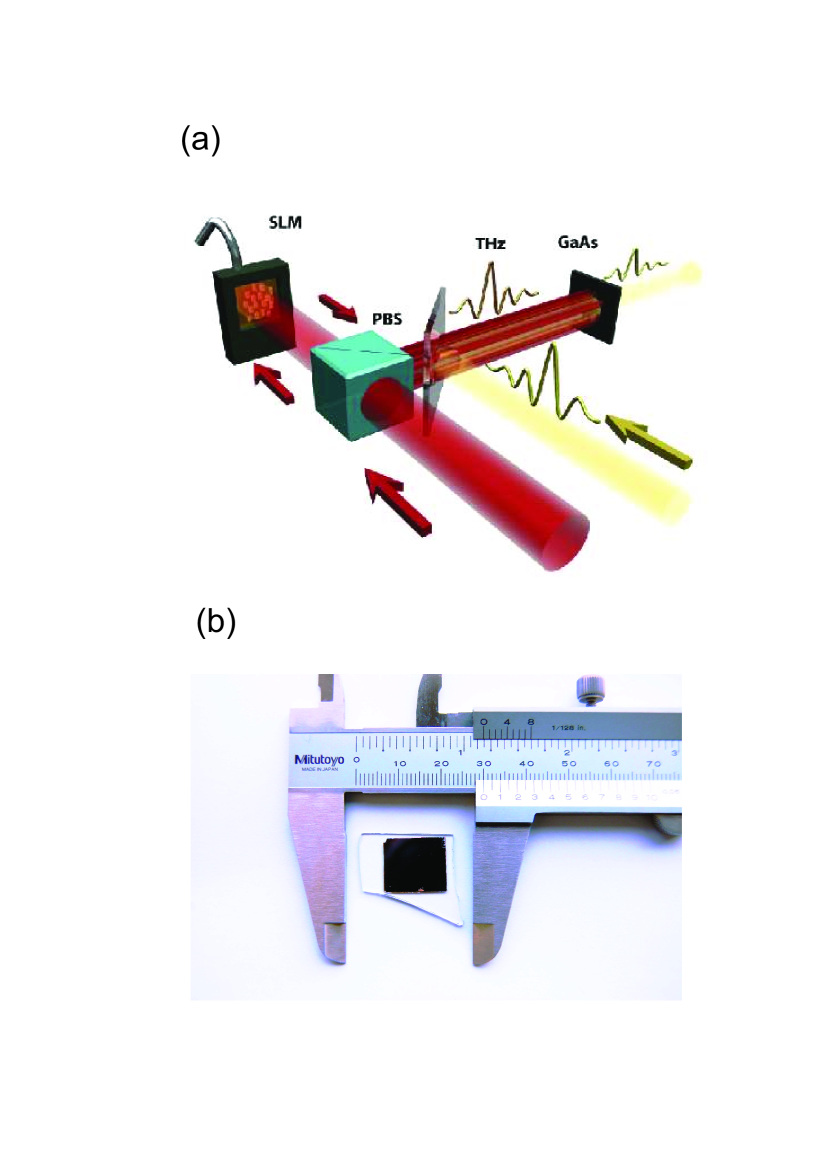
Setup and sample description. The measurements have been performed using time-resolved THz time-domain spectroscopy (see Methods). With this technique an optical pulse is used to pump a semiconductor while a time-delayed THz pulse probes the photo-induced changes in the conductivity of the semiconductor. A key element in our setup is a computer controlled SLM, which is used to structure the pump by spatially shaping the beam. The operation principle of the structured illumination is illustrated in Fig. 1(a). A horizontally polarized optical pulse ( nm), indicated by the red beam in the figure, is transmitted through a polarizing beam splitter (PBS) and reflected back by the SLM. The SLM is a pixelated liquid crystal device ( pixels), which rotates the polarization of the incident light. Light reflected from the so-called bright pixels undergoes a rotation of the polarization by , being reflected by the PBS towards the sample; while light reflected from dark pixels maintains its polarization and it is transmitted back through the PBS, thus not reaching the sample. The intensity of the light reflected by each pixel of the SLM and by the PBS can be changed continuously from a maximum value (bright pixel) to a minimum (dark pixel). A lens (not shown in Fig. 1(a)) with a focal length of is used to project (1:1) the structured beam onto the surface of the sample, which is a thin GaAs layer, where electrons are photo-excited from the valence to the conduction band only on the illuminated regions. A THz pulse, indicated by the yellow beam in Fig. 1(a), is made collinear with the optical pulse and transmitted through the sample. The pixel size on the surface of the sample is , being much smaller than the wavelength of THz radiation. Therefore, this technique is ideally suited for the optical generation of subwavelength THz structures.
The sample used for the experiments consists of a layer of single crystalline undoped GaAs with a thickness of 1 bonded to a substrate (see Methods). A photograph of the sample is shown in Fig. 1(b). Intrinsic GaAs has a dielectric behavior at THz frequencies. However, its real component of the permittivity becomes negative, hence GaAs becomes conducting, at 1 THz for carrier densities above . These carrier densities are easy to reach by pumping the sample with an optical pulse of moderate fluence. The high electron mobility of intrinsic GaAs at room temperature (), favors the excitation of localized SPPs. Moreover, the small thickness of the semiconductor slab, which is comparable to the optical absorption length of GaAs ( at nm), allows the (nearly) homogeneous excitation of carriers as a function of the depth in the layer. For the experiments we used pump fluences up to , which excites free carriers on the bright pixels of the illuminated pattern. The carrier density in GaAs at the regions illuminated by dark pixels is lower than . Therefore, optical pumping of GaAs with a shaped beam results into the local change of the permittivity from an insulating to a conducting state.
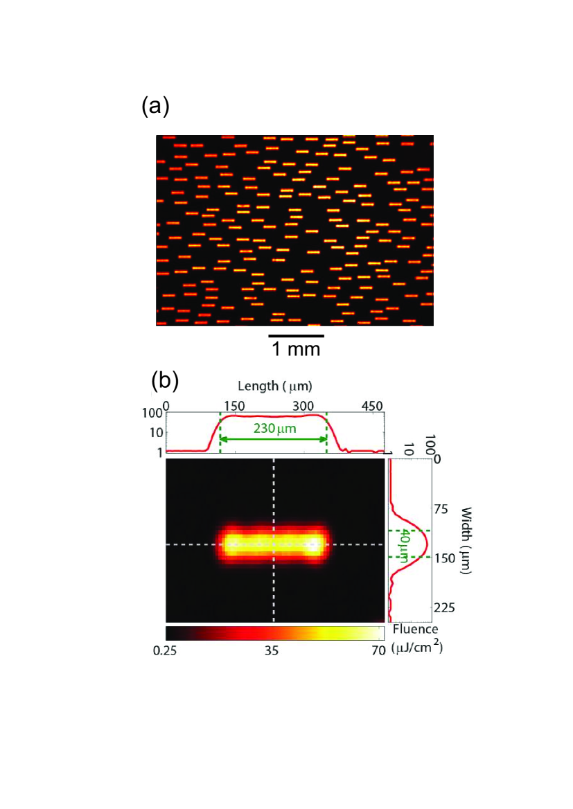
Photo-generated plasmonic antennas. To demonstrate the photo-generation of plasmonic antennas on the GaAs layer we have measured the THz extinction spectra of random arrays of rods with the same orientation generated with the same optical fluence and with different lengths; and of arrays of rods with the same length but generated with different fluences. Figure 2(a) shows an image of an array of rods. This image is taken by placing a CCD camera at the sample position. Their random distribution suppresses any effect due to periodicity in the THz extinction, while their horizontal alignment enables the excitation of localized SPPs for THz radiation incident with an horizontal polarization. A close view of a single plasmonic rod is shown in Fig. 2(b). The illuminated area (filling fraction of the rods) corresponds to 18% of the surface. The spacing between two consecutive rods was chosen to be larger than along the long axis of the rod and along the short axis. These distances are large enough to minimize the near field coupling between consecutive rods Muskens2007 , while maximizing their filling fraction to increase the THz extinction.
For the THz extinction measurements the sample was first illuminated with a pump pulse with a center wavelength nm and a duration of 100 fs. Subsequently, a THz pulse was transmitted through the sample. The time delay between the optical pump and the arrival of the THz pulse was ps, which is sufficiently long to enable the relaxation of hot electrons to the lowest energy state of the conduction band Beard2001 . Furthermore, this time delay was much shorter than the carrier recombination time, which was experimentally determined to be ps. The THz transmission amplitude is measured within a time window of 12 ps. Over this time window the carrier diffusion length is much shorter than all the characteristic lengths in the experiment, i.e., the dimensions of the structures and the THz wavelength. Therefore, the photo-excited plasmonic antennas can be described in a first approximation as having stationary dimensions and carrier density.
We measure the zeroth order differential transmission transients, , i.e., the THz amplitude transient transmitted through the optically pumped sample in the forward direction minus the transmitted transient of the unpumped sample . These measurements are done by chopping the pump beam at half the repetition rate of the laser, i.e., 500 Hz Ulbricht2011 . To gain spectral information about this transmission, the transients are Fourier transformed and squared to obtain the transmittance. The extinction , defined as the sum of scattering and absorption, is given according to the optical theorem as one minus the zeroth-order transmittance. The latter is equal to the ratio of the pumped to the unpumped transmittance . Therefore, .
Figure 3 is the main result of this manuscript. Figure 3 (a) shows the extinction spectra of photo-generated plasmonic rods with a fixed dimension of and varying optical pumping fluences. The polarization of the THz beam was set parallel to the long axis of the rods. A resonance appears in the extinction spectrum for optical fluences higher than 12 . At this fluence the number of photo-excited carriers in GaAs is large enough to give a metallic behavior to the semiconductor in the THz frequency range. The maximum extinction reaches values higher than 65% while the illuminated fraction of the GaAs is only 18%. This enhanced extinction can be explained in terms of the large THz scattering cross section of the rods resulting from their antenna like behavior. The resonance can be associated to the fundamental plasmonic mode, which occurs when the effective length of the rod is half the surface plasmon polariton wavelength, i.e., , where is the vacuum wavelength, the refractive index of the surface plasmon polariton defining its phase velocity Novotny2007 and is a parameter related to the field extension of the SPP outside the rod, which defines an effective rod length of Cubukcu2002 . The blue shift of the resonance as the pump fluence increases is a consequence of the increase in conductivity of the pumped GaAs. A larger conductivity results in a weaker penetration of the THz field in the pumped GaAs and a reduction of Novotny2007 .
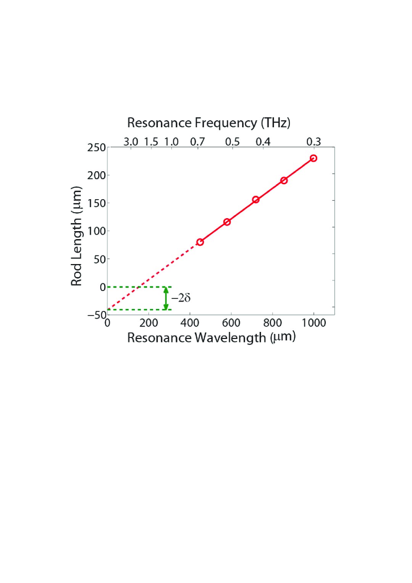
The extinction spectra of photo-generated plasmonic rods with various lengths and a fixed width of pumped at is shown in Fig. 3 (b). A significant redshift of the resonance and increase of the extinction is observed as the length of the photo-generated rods is increased. In Fig. 4 we plot the rod length as a function of the resonant wavelength of maximum extinction. From the slope of the linear fit, illustrated by the solid line, we obtain , while the intersection of this fit with the ordinate axis equals with .
A closer look to Fig. 3(b) reveals a shoulder at shorter wavelengths (around ) in the extinction spectrum of the longer rods. We attribute this shoulder, which is absent in the spectra of the shorter rods, to the excitation of the next higher order plasmonic mode in a rod by normal incident THz radiation, i.e., the mode Giannini2010 . The observation of multipolar photo-generated plasmonic modes is a consequence of the high quality of the GaAs layer used for the experiments.
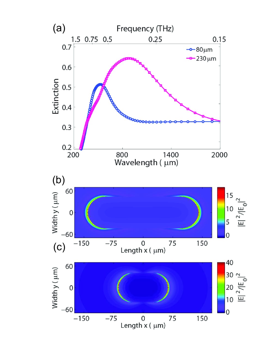
To further investigate the localized modes associated to the photo-generated rods, we have performed Finite Difference in Time Domain (FDTD) simulations using a commercial software package (Lumerical Solutions). Details on the simulations can be found in the Methods. Figure 5 (a) shows the extinction spectra of the 230 and 80 long rods. To approximate the simulated geometry as much as possible to the experiment, we have considered a graded variation of the carrier concentration in the GaAs film at the boundaries of the rod from at the core to in the unpumped surrounding region, which resembles the illumination profiles shown in Fig. 2(b). As can be appreciated in Fig. 5(a), this geometry reproduces reasonably well the resonance wavelength and magnitude of the extinction. Figures 5 (b) and (c) show the near field enhancement at the GaAs-air interface and at the wavelengths of the maximum extinction for the 230 and 80 long rods respectively. The enhancement, defined as the near field intensity normalized to the incident intensity at the GaAs-air interface, has the dipolar character expected for the mode in the rod-shaped antennas. The maximum field enhancement, which is larger for the shorter rods, is achieved at the edges of the rods where the charge density is maximum.
It is worthwhile to stress that the near-field enhancement in photo-generated plasmonic antennas can be fully controlled in magnitude and spatial position by simply changing the illumination pattern defined with the SLM. By controlling the time delay between the optical pump and THz probe pulse, it is also possible to tune the magnitude of the enhancement. This approach could be exploited to enhance the sensitivity of locally functionalized surfaces or to realize spectroscopy of subwavelength structures by resonant enhancement of the local fields. Moreover, larger field enhancements could be achieved by coupling rods to form dimers Schnell2009 or by defining bowtie antennas with sharp tips and small gaps Berrier2010 .
In conclusion, we have demonstrated the photo-generation of THz plasmonic materials by the structured illumination of a thin layer of undoped GaAs with arrays of micro-antennas. This illumination is accomplished with a spatial light modulator that allows a full optical control (spatial and temporal) of resonant frequencies and local field enhancements. This approach can probably be extended to the photo-generation of metamaterials exhibiting magnetic resonances, metasurfaces for active beam steering and THz wave guiding structures.
II Methods
GaAs layer Fabrication. The sample was prepared utilizing epitaxial growth in an Aixtron 200 low pressure metal organic chemical vapour deposition reactor and subsequent layer transfer. The epitaxial structure composed of a 10 nm thick sacrificial AlAs layer followed by a 1 thick undoped GaAs layer was grown at a temperature of 650 and a pressure of 20 mbar on a 2-inch diameter (001) GaAs wafer, 2 degrees off towards . Source materials were trimethyl-gallium and trimethyl-aluminium as group-III precursors and arsine as group V precursor. After growth a flexible plastic support carrier was mounted on top of the GaAs epi-layer and the sample was subjected to a HF solution in water for selective etching of the AlAs layer Voncken2004 . During the process the plastic carrier is used as a handle to bent away the GaAs epi-layer from the wafer ensuring optimal access of the HF solution to the 10 nm high etch front of the AlAs release layer Schermer2006 . After separation the GaAs thin-film is bonded to a 1 mm thick substrate using a mercapto-ester based polymer. The thickness of this bonding layer is approximately 40 . Finally the plastic support carrier is removed leaving the 1 single crystal GaAs layer on a SiO2 substrate.
Permittivity values. The values of the permittivity of the substrate and the bonding layer were experimentally determined in the frequency range of the measurements by measuring the time-domain THz transmission. This phase sensitive technique allows to obtain the complex permittivity from a single measurement provided that the thickness of the layers are precisely defined. These values of the permittivity are and for the bonding layer and the substrate, respectively. The permittivity of the GaAs layer could not be accurately determined in the same way due to its small thickness compared to the wavelength of THz radiation. Therefore, we approximate the permittivity of GaAs by that of a free electron gas described by the Drude model. This approximation has been proven to be valid for semiconductors at THz frequencies Beard2001 . The frequency dependent complex permittivity resulting from the Drude model of free charge carriers is given by
| (1) |
where both electron-electron and electron-phonon interactions are taken into account. The relative high and low (DC) frequency dielectric constants are and , respectively. Moreover, the transverse optical phonon absorption is at with a damping coefficient . The plasma frequency of GaAs is given by where is the carrier concentration per unit volume and is the effective electron mass. The e-e collision rate is given by , where is the carrier concentration dependent mobility, which can be approximated by the empirical relation Hilsum1974
| (2) |
Time-resolved THz time-domain spectroscopy. The measurements have been performed with a modified time-resolved THz time-domain spectrometer. With this pump-probe technique, a pulsed laser beam from an amplified oscillator ( nm, repetition rate = 1 KHz, pulse duration = 100 fs) is split in three beams. One of the beams is used to generate THz radiation by optical rectification in a 0.5 mm thick ZnTe crystal. The THz pulse is collected by parabolic gold mirrors and weakly focused onto the sample. The beam size onto the sample has a FWHM of 2.5 mm. The transmitted THz radiation is focused onto a 1 mm thick ZnTe crystal. The THz field amplitude in this crystal is probed by the second optical beam, which detects changes in the refractive index of the ZnTe crystal induced by the THz pulse (electro-optical sampling). By controlling the time delay between the optical beam generating the THz pulse and the optical beam probing the THz field amplitude, it is possible to measure the THz amplitude transients. These transients can be Fourier transformed to obtain the amplitude or the power spectra. The third optical beam in the setup is used as an optical pump for the sample. Controlling the time delay between the optical pump and the THz pulse probing the sample allows an accurate investigation of carrier dymanics in photo-excited samples Ulbricht2011 .
FDTD simulations. The extinction and near fields were simulated using a commercial 3D - Finite Difference in Time Domain (FDTD) software. The simulated structures were chosen to be as close as possible to the experimental conditions, i.e., a multi-layered structure consisting of air - silicon oxide - bonding polymer - GaAs - air. The experimentally determined values of the permittivity of the bonding layer and the substrate were used for the simulations. An homogeneous carrier concentration was considered through the thickness of 1 of the GaAs layer. The illuminated rods were simulated by considering a rectangular region with rounded corners and a permittivity given by the Drude model. A graded illumination across the edges of the rods (see side graphs in Fig. 2(b)) was taken into account by considering consecutive shells with varying thickness of and a reduced carrier density as the shell dimensions is increased. The carrier density in the innermost region of the rod is , while the outermost shell has . The non-illuminated GaAs was assumed to have to take into account the finite contrast between bright and dark pixels in the structured illumination. For the simulations we used a total field scattered field source, a perfectly matched layer as boundary of the simulated volume and a transmission monitor to determine the extinction. The simulated transmission was corrected by the rod filling fraction to compare quantitatively to the experiments.
Acknowledgements.
We are thankful to M.C. Schaafsma and J. Versluis for valuable discussions. This work has been supported by the ERC through grant no 259727 THZ-PLASMON and by the Netherlands Foundation for Fundamental Research on Matter (FOM) and the Netherlands Organisation for Scientific Research (NWO)References
- (1) T.W. Ebbesen, H.J. Lezec, H.F. Ghaemi, T. Thio, P. A. Wolff, Extraordinary optical transmission through sub-wavelength hole arrays, Nature 391 667-669 (1998)
- (2) W.L. Barnes, A. Dereux, and T.W. Ebbesen, Surface plasmon subwavelength optics, Nature 424, 824-830 (2003).
- (3) J.A. schuller, E.S. Barnard, W. Cai, Y.C. Jun, J.S White and M.L. Brongersma, Plasmonics for extreme light concentration and manipulation, Nature Mat. 9, 193-204 (2010).
- (4) J. Gómez Rivas, C. Schotsch, P.H. Bolivar, and H. Kurz, Enhanced transmission of THz radiation through subwavelength holes, Phys. Rev. B 68, 201306 (2003).
- (5) D. Qu, D. Grischkowsky, and W. Zhang, Terahertz transmission properties of thin sub wavelength metallic hole arrays, Opt. Lett. 29, 896-898 (2004).
- (6) H. Cao and A. Nahata, Resonantly enhanced transmission of terahertz radiation through a periodic array of sub wavelength apertures, Opt. Express 12 , 1004-1010 (2004).
- (7) M.A. Seo, H.R. Park, S.M. Koo, D.J. Park, J.H. Kang, O.K. Suwal, S.S. Choi, P.C.M. Planken, G.S. Park, N.K. Park, Q. H. Park, and D. S. Kim, Terahertz field enhancement by a metallic nano slit operating beyond the skin-depth limit, Nature Phot. 3, 152-156 (2009)
- (8) M.I. Stockman, M.F. Kling, U. Kleineberg, and F.Krausz, Attosecond nanoplasmonic-field microscope , Nature Photonics 1, 539-544 (2007).
- (9) M. Aeschlimann, M. Bauer, D. Bayer, T. Brixner, F. Javier García de Abajo, W. Pfeiffer, M. Rohmer, C. Spindler, and F. Steeb, Adaptive subwavelength control of nano-optical fields, Nature 446, 301-304 (2007).
- (10) G. Volpe, S. Cherukulappurath, R.J. Parramon, G. Molina-Terriza, and R. Quidant, Controlling the Optical Near Field of Nanoantennas with Spatial Phase-Shaped Beams, Nano Letters 9, 3608-3611 (2009).
- (11) B. Gjonaj, J. Aulbach, P.M. Johnson, A.P. Mosk, L. Kuipers and A. Lagendijk, Active spatial control of plasmonic fields, Nature Photon. 5, 360-363 (2011).
- (12) T. S. Kao , E.T.F. Rogers , J.Y. Ou , and N.I. Zheludev, Digitally Addressable Focusing of Light into a Subwavelength Hot Spot, Nano Lett. 12 2728-2731 (2012).
- (13) M. Perner, P. Bost, U. Lemmer, G. von Plessen, J. Feldmann, U. Becker, M. Mennig, M. Schmitt, and H. Schmidt, Optically Induced Damping of the Surface Plasmon Resonance in Gold Colloids, Phys. Rev. Lett 78, 2192-2195 (1997).
- (14) S. Link and M.A. El-Sayed, Spectral Properties and Relaxation Dynamics of Surface Plasmon Electronic Oscillations in Gold and Silver Nanodots and Nanorods, J. Phys. Chem B 103, 8410-8426 (1999).
- (15) N. Rotenberg, M. Betz and H. M. van Driel, Ultrafast control of grating-assisted light coupling to surface plasmons, Opt. Lett. 33, 2137-2139 (2008).
- (16) V. Halté, A. Banabbas, and J.-Y. Bigot, Surface plasmon dynamics in arrays of subwavelength holes: the role of optical interband transitions, Opt. Express 16, 11611-11617 (2008).
- (17) K.F. MacDonald, Z.L. Samson, M.I. Stockman and N.I. Zheludev, Ultrafast active plasmonics, Nature Photonics 3, 55-58 (2009).
- (18) V.V. Temnov, K.A. Nelson, G. Armelles, A. Cebollada, T. Thomay, A. Leitenstorfer and R. Bratschitsch, Femtosecond surface plasmon interferometry Opt. Express 17, 8423-8432 (2009).
- (19) J. Dintinger, I. Robel, P.V. Kamat, C. Genet, and T.W. Ebbesen,Terahertz all-optical molecule-plasmon modulation Adv. Mater. 18, 1645-1648 (2006).
- (20) S. J. Allen, D. C. Tsui, and R. A. Logan, Observation of the Two-Dimensional Plasmon in Silicon Inversion Layers, Phys. Rev. Lett. 38, 980-983 (1977)
- (21) J. Gómez Rivas, M. Kuttge, P. Haring Bolivar, H. Kurz, and J.A. Sanchez-Gil, Propagation of surface plasmon polaritons on semiconductor gratings, Phys. Rev. Lett. 93, 256804 (2004)
- (22) J. Gómez Rivas, Terahertz : the art of confinement, Nature Photon. 2, 137-138 (2008).
- (23) J. Gómez Rivas, M. Kuttge, H. Kurz, P. Haring Bolivar, and J.A. S·nchez-Gil, Low-frequency active surface plasmon optics on semiconductors, Appl. Phys. Lett. 88, 082106 (2006).
- (24) H.T. Chen, W.J. Padilla, J.M.O. Zide, A.C. Gossard, A.J. Taylor, and R.D. Averitt, Active terahertz metamaterial devices, Nature 444, 597-600 (2006).
- (25) H.T. Chen, HT, J.F. O’Hara, A.K. Azad, AK, A.J. Taylor, R.D. Averitt, D.B. Shrekenhamer, W.J. Padilla, Experimental demonstration of frequency-agile terahertz metamaterials, Nature Photonics 2, 295-298 (2008).
- (26) A. Berrier, R. Ulbricht, M. Bonn, and J. Gómez Rivas, Ultrafast active control of localized surface plasmon resonances in silicon bowtie antennas, Opt. Express 18, 23226-23235 (2010).
- (27) T. Okada, K. Ooi, and Y. Nakata, and K. Fujita, Direct creation of a photoinduced metallic structure and its optical properties in the terahertz frequency region, Opt. Lett. 10, 1719-1721 (2010).
- (28) T. Okada and K. Tanaka, Photo-designed terahertz devices, Sci. Rep. 1, 121; DOI:10.1038/srep00121 (2011).
- (29) I. Chatzakis, P. Tassin, L. Luo, N.-H. Shen, L. Zhang, J. Wang, T. Koschny, and C. M. Soukoulis, One- and two-dimensional photo-imprinted diffraction gratings for manipulating terahertz waves, Appl. Phys. Lett. 103, 043101 (2013).
- (30) S. Busch, B. Scherger, M. Scheller, and M. Koch, Optically controlled terahertz beam steering and imaging, Opt. Lett. 8, 1391-1392 (2012).
- (31) C. Rizza, A. Ciattoni, L. Columbo, M. Brambilla, and F. Prati, Terahertz optically tunable dielectric metamaterials without microfabrication, Opt. Lett. 38, 1307-1309 (2013).
- (32) O.L. Muskens, V. Giannini, J.A Sánchez-Gil, and J. Gómez Rivas, Optical scattering resonances of single and coupled dimer plasmonic nanoantennas, Opt. Express 15, 17736-17746 (2007).
- (33) M.C. Beard, G.M. Turner, and C.A. Schmuttenmaer, Subpicosecond carrier dynamics in low-temperature grown GaAs as measured by time-resolved terahertz spectroscopy, J. Appl. Phys. 90, 5915-5923 (2001).
- (34) L. Novotny, Effective wavelength scaling for optical antennas, Phys. Rev. Lett. 98, 266802 (2007)
- (35) E. Cubukcu and F. Capasso, Optical nanorod antennas as dispersive one-dimensional Fabry P rot resonators for surface plasmons, Appl. Phys. Lett. 95 201101 (2009).
- (36) V. Giannini, G. Vecchi and J. Gómez Rivas, Lighting up multipolar surface plasmon polaritons by collective resonances in arrays of nanoantennas, Phys. Rev. Lett. 105, 266801 1-4 (2010).
- (37) M. Schnell, A. Garcia-Etxarri, A. J. Huber, K. Crozier, J. Aizpurua, and R. Hillenbrand, Controlling the near-field oscillations of plasmonic nanoatennas, Nature Phot. 3, 287 (2009).
- (38) W.J. Padilla, A.J. Taylor, C. Highstrete, M. Lee, and R. D. Averitt Dynamical electric and magnetic metamaterial response at terahertz frequencies, Phys. Rev. Lett. 96, 107401 (2006).
- (39) M.M.A.J. Voncken, J.J. Schermer, A.T.J. van Niftrik, G.J. Bauhuis, P. Mulder, P.K. Larsen, T.P.J. Peters, B. de Bruin, A. Klaassen, and J.J. Kelly, Etching AlAs with HF for epitaxial lift-off applications, J. Electrochem. Soc. 151, G346-G351 (2004).
- (40) J.J. Schermer, G.J. Bauhuis, P. Mulder, E.J. Haverkamp, J. van Deelen, A.T.J. van Niftrik, and P.K. Larsen, Photon confinement in high-efficiency, thin-film III V solar cells obtained by epitaxial lift-off, Thin Solid Films 511-512 645-653 (2006).
- (41) C. Hilsum, Simple empirical relationship between mobility and carrier concentration, Electron. Lett. 10 259-260 (1974)
- (42) R. Ulbricht, H. Euan, J. Shan, T. Heinz, and M. Bonn, Carrier dynamics in semiconductors studied with time-resolved terahertz spectroscopy, Rev. Mod. Phys. 83, 543-586 (2011).