Structural manipulation of the graphene/metal-interface with Ar+ irradiation
Abstract
Controlled defect creation is a prerequisite for the detailed study of disorder effects in materials. Here, we irradiate a graphene/Ir(111)-interface with low-energy Ar+ to study the induced structural changes. Combining computer simulations and scanning-probe microscopy, we show that the resulting disorder manifests mainly in the forms of intercalated metal adatoms and vacancy-type defects in graphene. One prominent feature at higher irradiation energies (from 1 keV up) is the formation of line-like depressions, which consist of sequential graphene defects created by the ion channeling within the interface—much like a stone skipping on water. Lower energies result in simpler defects, down to 100 eV where more than one defect in every three is a graphene single vacancy.
pacs:
81.05.ue, 68.37.Ef, 61.80.-x, 31.15.xvI Introduction
Measurements of the properties of graphene, especially the electronic transport characteristics castro_neto_electronic_2009 , have yielded results which deviate from the theory geim_rise_2007 . These discrepancies are likely to have partially risen from disorder, introduced either already in growth or later during sample preparation. A detailed correlation between the atomic-level disorder and the corresponding change in the properties requires a controlled way of creating defects. On the other hand, defects can also be beneficial for nanoengineering low-dimensional structures krasheninnikov_engineering_2007 .
One way for manipulating structures is to employ beams of energetic particles, for example ions. While ion irradiation effects in conventional materials have been studied for decades, we are only starting to fully understand the irradiation-response of low-dimensional structures. In the case of suspended graphene, some of the authors of the present work have recently conducted atomic-level theoretical studies of irradiation effects for various ions lehtinen_effects_2010 ; lehtinen_cutting_2011 ; ahlgren_ion_2012 . For supported graphene, experimental studies have been carried out for irradiation with 140 eV Ar+ on Pt(111) ugeda_point_2011 and SiC(0001) ugeda_electronic_2012 surfaces, 30 keV and 100 keV Ar+ on SiO2 substrate tapaszto_tuning_2008 ; kalbac_ion-irradiation-induced_2013 , and 5 keV Xe+ on Ir(111) surface (at a grazing angle) standop_ion_2013 . Ion irradiation has already been demonstrated to tune the electronic and magnetic properties of graphene tapaszto_tuning_2008 ; chen_defect_2009 ; nair_spin-half_2012 ; nair_dual_2013 , and to create single ugeda_point_2011 and double vacancies ugeda_electronic_2012 , although no direct correlation between the properties and defect structures has been carried out. Overall, as far as we know, no atomic-level analysis of irradiation-induced structural changes at varying irradiation energies has been reported for supported graphene.
In this study, we investigate Ar+ irradiation effects on graphene on a weakly interacting metal substrate, Ir(111), by combining atomistic simulations and scanning tunneling microscopy (STM). Good qualitative agreement between the methods (over all experimentally studied irradiation energies: 0.1 keV, 0.3 keV and 1 keV) allows us to assign the experimentally observed disorder to intercalated adatoms and disordered graphene areas. According to simulations, as compared to suspended graphene, the substrate leads to more complex defect structures at all studied energies (up to 30 keV). Nevertheless, at the lowest studied energy above the damaging threshold (100 eV), more than every third created defect is a single vacancy in graphene. Below 1 keV the substrate somewhat protects graphene, whereas above 1 keV backscattered metal atoms increase the damage. At similar energies, ion channeling below the graphene sheet starts to occur, leading to line-like features of small vacancy-type graphene defects. Such large variations in the introduced disorder as a function of the ion energy, already at the relatively small energy range of 100 eV—1 keV, show a great promise for ion irradiation-mediated manipulation of graphene/metal-interfaces.
II Methods and results
We used a Createc LT-STM system for the Ar+ irradiation experiments (base pressure around mbar). Following the procedure outlined in Ref. coraux_growth_2009 , graphene growth was initiated by absorbing a mono-layer of ethylene on a clean Ir(111) surface. The sample was then heated to 1670 K for 30 s, which resulted in large ( nm) virtually defect-free graphene islands. We calibrated the irradiation current with a sample bias of 40 V to reduce distortion due to secondary electrons (100 nA was used for all samples). Taking the beam profile and sample size into account, this equals to impacts per nm2 per minute. Despite this uncertainty, arising from the unknown exact beam profile, the relative dose should vary very little between different samples. The irradiation was carried out perpendicular to the graphene sheet.
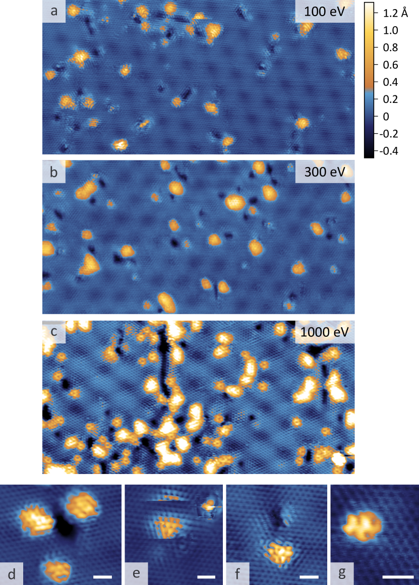
Atomic-resolution images showing the introduced disorder at different experimentally studied energies (0.1, 0.3, and 1.0 keV) are presented in Fig. 1a-c with higher magnification example images of selected prominent features (Fig. 1d-g). Irradiation time was one minute at 0.1 keV and 0.3 keV, and half a minute at 1.0 keV. Two kinds of features appear in the images: darker depressed areas and adjacent bright protrusions. We initially interpret the depressions as defects where carbon atoms have bound to the substrate and the protrusions as metal adatoms intercalated under the graphene layer. Similar interpretation was recently made by Standop et al. standop_ion_2013 .
Next, we turned to molecular dynamics (MD) to verify our interpretation of the observed features. We followed the same approach as in our previous studies for carbon nanotubes tolvanen_relative_2007 and graphene (both suspended lehtinen_effects_2010 ; lehtinen_cutting_2011 ; ahlgren_ion_2012 and supported standop_ion_2013 ). In our model, we replaced the iridium substrate with platinum (as in Ref. standop_ion_2013 ), because of the similarity of platinum and iridium in mass, structure and chemistry, and because well-established interaction models exist for Pt-Pt and Pt-C albe_modeling_2002 , unlike for Ir-Ir and Ir-C. The substrate contained 45,900 atoms set below a graphene structure (2,584 atoms) at a distance of 3.31 Å. For C-C, we used the Brenner potential brenner_second-generation_2002 , whereas the Ar+ interactions were described with a universal repulsive potential ziegler_stopping_1985 (no actual charge state was considered). Approximately 300 impact points were randomly selected for each energy. We considered only energies keV to ensure that nuclear scattering dominates as the damage mechanism lehtinen_cutting_2011 . The simulations were carried out at 0 K for 5 ps, which was enough to prevent further bonding changes close to the interface area (energy was dissipated at the edges using the Berendsen thermostat berendsen_molecular_1984 ). After each event, we relaxed the atomic structure before the analysis. To check the effect of possible spurious structures, we conducted a further annealing study (800 K, 1 ns) for the 1 keV cases. The results did not significantly change, except for occasional splitting of larger defects into smaller ones with approximately the same total area and increasing bonding between the defects and the substrate. We also extended our earlier simulations for suspended graphene lehtinen_effects_2010 for a direct comparison with the present study.
We start the discussion of simulation results from the analysis of disorder created in graphene due to the impacts (Fig. 2a). We categorized the damage into single vacancies (sv), double vacancies (dv), and other defects (identified by lost six-membered carbon rings in graphene). The probability to create a defect increases from zero below 100 eV up to a maximum at about 1 keV, after which it decreases because of the decreasing scattering cross section at high energies. At the lowest energies (above 30 eV), a significant proportion of the created defects are sv with a small probability for dv, in agreement with experimental observations of these defects in graphene irradiated with 140 eV Ar+ on Pt(111) and SiC(0001) surfaces ugeda_point_2011 ; ugeda_electronic_2012 . At increasing energies the share of sv’s decreases while more complex defects gain prominence.
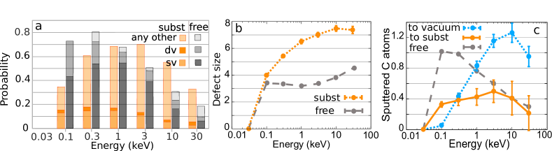
Comparing the results between supported and suspended graphene, it is clear that the substrate leads to more complex defect structures. However, at lower energies, it decreases the overall damaging probability. This happens because the substrate stops the displaced low-energy carbon atoms before they are completely detached from the graphene sheet. This trend becomes reversed at higher energies (around 1 keV), because of the energy deposited on the top layers of the substrate, which leads to displacement of metal atoms. These atoms then contribute to the defect production in graphene. At the highest studied energy (30 keV) the difference between supported and suspended graphene starts to fade, since the bulk of the energy of the impinging ions is deposited deep into the substrate.
The average defect size in graphene is shown in Fig. 2b as a function of the ion energy. As could be expected, we see an increase in the defect size with increasing ion energy, but only for supported graphene, where both sputtering from the substrate and binding to it contribute to the defect creation. For suspended graphene, the values first rise to about three hexagonal carbon rings (which is the size of a sv; one missing atom) per defect at the energy of 0.1 keV, and then remain almost constant. This leveling out occurs because the ion impact can only displace one or two carbon atoms, which typically scatter away from the graphene plane upon further collisions, except at very high energies (tens of keV).
We further analyzed the sputtering from graphene (Fig. 2c) both towards the substrate and to the surrounding vacuum. This data follows the same trend as the damaging probability, however peaking at close to 10 keV. In contrast, the maximum sputtering yield for suspended graphene is reached at a significantly lower energy (close to 100 eV). The reason for this is the same as previously described: at low energies the substrate stops the displaced carbon atoms, resulting in a lower sputtering yield. However, at high energies metal atoms displaced from the substrate can also detach atoms from graphene. Interestingly, after the initial onset at 0.1 keV, the number of carbon atoms sputtering to the substrate remains relatively constant at about 0.4 atoms/ion throughout the studied energy range. This region coincides with the plateau in the average defect size in the case of suspended graphene (Fig. 2b), because both result mainly from carbon atoms displaced by the primary or secondary collisions during the initial ion impact in the direction of the substrate.
Next, we turn to look at what happens to the Ar+ ions after the impact. We limit our analysis to the interface region, as only those ions which remain at the very top of the substrate or intercalated under graphene can be experimentally detected at the relatively low ion doses used in this study. We classify any ion located at the top of the substrate or within 0.5 nm above it as an adatom (note that the Ar+-C and Ar+-Pt interactions in our simulations are purely repulsive). Average number of these adatoms per impinging ion is shown as a function of ion energy in Fig. 3a. At 30 eV (the lowest studied energy), the ion lacks the energy required to penetrate graphene, and is therefore always reflected back to the vacuum. However, at 0.1 keV, already more than 20% of the ions become trapped at the interface. The probability increases up to about 50% at 0.3 keV before decreasing again due to deeper penetration into the substrate. At experimental timescales (beyond our computational reach), the Ar adatoms can also escape through larger openings in the graphene sheet, more of which are created at higher energies (see Fig. 2b).
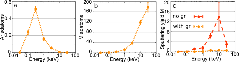
We also counted the substrate atoms which were elevated above the surface due to ion impacts (all atoms within 0.5 nm above the top of the substrate were included). Average number per impact is shown as a function of ion energy in Fig. 3b. The increase is linear up to 10 keV, after which the rate of increase decreases (note the logarithmic -axis in the plot). Obviously, several of those metal atoms trapped between graphene and the substrate would have sputtered into vacuum, were there no graphene on top of the metal. To get a better understanding on the role of graphene in suspending metal sputtering, we further calculated the sputtering yield of both graphene-covered and naked substrates as a function of the ion energy (Fig. 3c). Clearly, graphene stops almost all sputtering from the substrate, similar to what was found in the case of grazing angle irradiation standop_ion_2013 . Only above 1 keV some of the sputtered metal atoms penetrate the graphene sheet, resulting in a slight deviation from zero in the graph. This is in strong contrast with sputtering yields above 10 atoms/ion observed at intermediate energies for the naked metal substrate.
III Discussion
To allow for a direct comparison between the simulations and the experiments, we estimated the areal coverage of both the protrusions and the suppressions from the STM images (Fig. 1) at all three energies. At 0.1 keV, the latter cover approximately 1% of the area, corresponding to about nm2 per impact. The coverage is twice as high (2%) at 0.3 keV. At 1.0 keV, the coverage (with half the dose) is about 3%, corresponding to about nm2 per impact. The corresponding simulation results are in a very good agreement with these estimates, being 0.036 nm2, 0.086 nm2 and 0.117 nm2, respectively (assuming they correspond to disorder in graphene, see Fig. 2a,b). The coverage of protrusions, as estimated from the STM images, are 6.0%, 7.6% and 12% at 0.1 keV, 0.3 keV and 1.0 keV, respectively. Corresponding relative ratios, as compared to the 1 keV case, and taking into account the dose for each case, are 0.25, 0.32 and 1.00. These can be compared to the number of Ar and metal atoms in the interface area in the simulations (see Fig. 3a,b), which yield ratios of 0.09, 0.36 and 1.00. The discrepancy at 0.1 keV can be at least partially due to point defects ugeda_point_2011 ; ugeda_electronic_2012 that appear as protrusions in STM images (see also Fig. 1f,g) and/or Ar adatoms, which are trapped at the interface and only observed at 0.1 keV in the experiments (see Fig. 1d and Supplementary Material presented below). Simulations indicate some Ar adatoms also at 0.3 keV and 1.0 keV, which we expect to be due to the short time scale, which does not allow the atoms to escape through larger holes in graphene created at higher energies. Both of these effects would increase the apparent ratio of protrusions at 0.1 keV, as compared to higher energies.
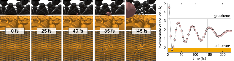
Finally, we also point out the long line-like depressions, which appear in the STM images after 1 keV irradiation (for an example, see Fig. 1c). These defects are remarkably similar to the ion tracks caused by grazing-angle irradiation standop_ion_2013 , which can be turned into a graphene nanomesh via high-temperature annealing. Although counter-intuitive for perpendicular irradiation, as in our case, it turns out that the formation mechanism is exactly the same in both cases: the incoming ion is occasionally deflected into the interface area between the substrate and graphene, and causes a line of small vacancy-type defects to form while channeling between the two materials (see Fig. 4 and Supplementary Material).
IV Conclusions
As a conclusion, we have carried out a study of Ar+ irradiation of graphene on a metal substrate combining atomistic simulations and scanning-probe microscopy. Our results show that the presence of a substrate leads to more complicated defect structures as compared to suspended graphene, and that the complexity of the created defects can be controlled via irradiation energy: on the one hand, at 1 keV, even irradiation perpendicular to the graphene sheet leads to formation of line-like defects via interface channeling of the impinging ion; on the other hand, lower energies result in simpler defects, such as single vacancies in graphene (up to one third of the defects at 100 eV). Our results provide a basis for controlled introduction of disorder into graphene on a metal substrate, and may open the way towards graphene-metal interface structures with tailored properties.
Acknowledgments
We acknowledge Austrian Science Fund (FWF): M 1481-N20, Helsinki University Funds, the European Research Council (ERC-2011-StG No. 278698 ”PRECISE-NANO”), the Finnish Academy of Science and Letters, the Academy of Finland (Centre of Excellence in Low Temperature Quantum Phenomena and Devices No. 250280) and the Finnish Cultural Foundation for funding. Further, we acknowledge CSC Finland and Vienna Scientific Cluster for generous grants of computational resources. We also thank Arkady Krasheninnikov and Carsten Busse for insightful discussions.
References
- (1) A. Castro Neto, F. Guinea, N. Peres, K. Novoselov, and A. Geim, Rev. Mod. Phys. 81, 109–162 (2009).
- (2) A. K. Geim and K. S. Novoselov, Nat. Mater. 6, 183–191 (2007).
- (3) A. V. Krasheninnikov and F. Banhart, Nature Mater. 6, 723–733 (2007).
- (4) O. Lehtinen, J. Kotakoski, A. V. Krasheninnikov, A. Tolvanen, K. Nordlund, and J. Keinonen, Phys. Rev. B 81, 153401 (2010).
- (5) O. Lehtinen, J. Kotakoski, A. V. Krasheninnikov, and J. Keinonen, Nanotechnology 22, 175306 (2011).
- (6) E. H. Åhlgren, J. Kotakoski, O. Lehtinen, and A. V. Krasheninnikov, Appl. Phys. Lett. 100, 233108 (2012).
- (7) M. M. Ugeda, D. Fernandez-Torre, I. Brihuega, P. Pou, A. J. Martinez-Galera, R. Perez, and J. M. Gomez-Rodriguez, Phys. Rev. Lett. 107, 116803 (2011).
- (8) M. M. Ugeda, I. Brihuega, F. Hiebel, P. Mallet, J.-Y. Veuillen, J. M. Gomez-Rodriguez, and F. Yndurain, Phys. Rev. B 85, 121402 (2012).
- (9) L. Tapaszto, G. Dobrik, P. Nemes-Incze, G. Vertesy, P. Lambin, and L. P. Biro, Phys. Rev. B 78, 233407 (2008).
- (10) M. Kalbac, O. Lehtinen, A. V. Krasheninnikov, and J. Keinonen, Adv. Mater. 25, 1004–1009 (2013).
- (11) S. Standop, O. Lehtinen, C. Herbig, G. Lewes-Malandrakis, F. Craes, J. Kotakoski, T. Michely, A. V. Krasheninnikov, and C. Busse, Nano Lett. 13, 1948-1955 (2013).
- (12) J.-H. Chen, W. G. Cullen, C. Jang, M. S. Fuhrer, and E. D. Williams, Phys. Rev. Lett. 102, 236805 (2009).
- (13) R. R. Nair, M. Sepioni, I.-L. Tsai, O. Lehtinen, J. Keinonen, A. V. Krasheninnikov, T. Thomson, A. K. Geim, and I. V. Grigorieva, Nature Phys. 8, 199–202 (2012).
- (14) R. R. Nair, I.-L. Tsai, M. Sepioni, O. Lehtinen, J. Keinonen, A. V. Krasheninnikov, A. H. Castro Neto, M. I. Katsnelson, A. K. Geim, and I. V. Grigorieva, Nat. Comm. 4, 2010 (2013).
- (15) J. Coraux, A. T. N’Diaye, M. Engler, C. Busse, D. Wall, N. Buckanie, F.-J. M. Z. Heringdorf, R. van Gastel, B. Poelsema, and T. Michely, New J. Phys. 11, 023006 (2009).
- (16) A. Tolvanen, J. Kotakoski, A. V. Krasheninnikov, and K. Nordlund, Appl. Phys. Lett. 91, 173109 (2007).
- (17) K. Albe, K. Nordlund, J. Nord, and A. Kuronen, Phys. Rev. B 66, 035205 (2002).
- (18) D. Brenner et al., J. Phys. Cond. Matt. 14, 783 (2002).
- (19) J. F. Ziegler, J. P. Biersack, and U. Littmark, The Stopping and Range of Ions in Solids (Pergamon, New York, 1985).
- (20) H. J. C. Berendsen, J. P. M. Postma, W. F. Van Gunsteren, A. DiNola, and J. R. Haak, J. Chem. Phys. 81, 3684 (1984).
- (21) C. J. Powell and A. Jablonski, NIST Electron Effective-Attenuation-Length Database, Version 1.3, SRD 82 National Institute of Standards and Technology, Gaithersburg, MD (2011).
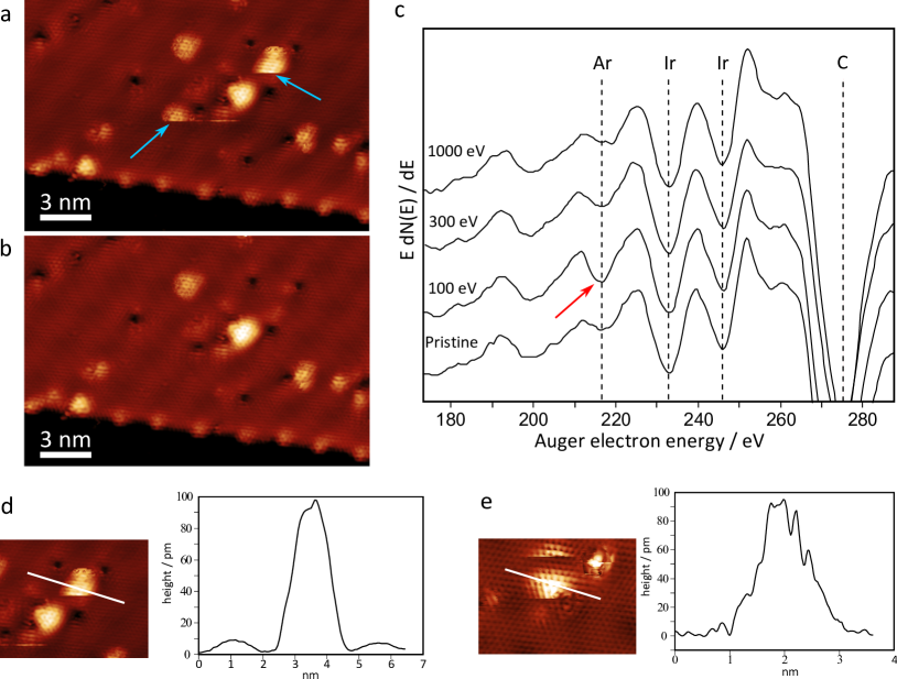
Appendix A Supplementary Material
This supplement contains additional experimental images and spectra of the Ar adatoms observed under the graphene sheet after 100 eV irradiation.
Figs. 5a and 5b show two consecutive STM scans (scan direction down) where two protrusions (marked by blue arrows) disappear from under the STM tip while scanning. Unlike in Fig. 1a of the main article, where the protrusion moved back and forth while scanning, here the protrusions disappear completely. Our interpretation is that the intercalated Ar adatoms are pushed out through holes in the graphene sheet. The apparent STM height of all mobile protrusions is about 1 Å (see Fig. 5 d,e).
To provide further evidence that the mobile protrusions we see are actually intercalated Ar atoms, we measured Auger electron spectra (AES) of samples irradiated with different energies with the same absolute dose (Fig. 5c). The spectra were acquired in situ with a Perkin Elmer 15-255G double pass cylindrical mirror analyzer (DPCMA) using a 3 keV electron beam. The dip in the derivative spectrum at the Ar LMM transition is clearly the largest in the 100 eV sample and diminishes almost completely with increasing energy. The AES signal of the Ar LMM transition comes from the few top atomic layers, as the effective attenuation length of the Auger electrons in iridium is only 4 Å powell_nist_2011 . Hence the AES data shows that as the ion energy increases, Ar is deposited deeper into the sample. To ensure a measurable Ar signal, the AES experiments were conducted with a slightly higher dose, compared to the STM experiments.