Dissipation mechanism above the current threshold in Josephson junction chains
Abstract
We present measurements on one-dimensional Josephson junction arrays formed by a chain of SQUID loops in the regime where . We observe a blockaded zero current branch for small bias voltages. Above a certain voltage the - characteristics changes discontinuously to a dissipative branch characterized by a flux dependent conductance. Three of four samples show a pronounced hysteresis for a forward and backward voltage sweep. We observe a periodic field dependence of the conductance above which can be described with theory for cooper-pairs and therefore gives evidence of viscous dynamics of Cooper pair transport through the array.
The physics of small single superconducting islands connected via the Josephson effect to an environment is well understood in various regimes and can be used as a building block for more complex systems. For low dimensional arrangements of these islands one finds remarkable similarities to other research areas. For example, the suppression of the electrical conductance in one or two dimensional ultra thin superconducting granular films Goldman and Markovic (1998) is also observed in long arrays of superconducting nano-islands. Another intriguing example is the projected quantum mechanical duality of solitonic single fluxon excitations observable in long Josephson contacts to the charge transport in series of small capacitance superconducting islands Haviland and Delsing (1996); Hermon et al. (1996); Rachel and Shnirman (2009); Homfeld et al. (2011).
(a)
 (b)
(b)
 (c)
(c)
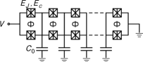
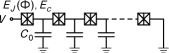
In this paper we report on measurements on nano-structured one dimensional chains of superconducting islands, connected via Josephson tunnel junctions (JJ) (for a sketch, see Fig. 1). The islands are characterized by a small self capacitance which is dominated by the capacitance of the Josephson junctions and a small contribution () originating from the metallic environment held at ground potential. Due to the size of fF the corresponding charging energy of one island is large, at operation temperatures below 0.1K. Thermally activated processes are strongly suppressed. From a conductance point of view, is in turn in competition with the Josephson coupling energy . In the limit the array behaves entirely superconducting, manifested, e.g., in a supercurrent at zero voltage Chow et al. (1998); Agren et al. (2001), whereas for the desired zero current state is observable at finite voltages Haviland and Delsing (1996). From the normal state conductance above the Ambegaokar-Baratoff relationAmbegaokar and Baratoff (1963a); *ambegaokar63e is helpful for an estimate of the Josephson coupling energy of on island to the next. Here is the superconducting gap energy, the conductance in units of and is the number of JJ. Both the capacitance and are proportional to the junction area of a Josephson contact.
For shadow-evaporated Al/AlOx/Al tunnel junctions, employed in this work, the regime can easily be reached. Furthermore, it is convenient to implement the Josephson junctions in the shape of SQUID loops as indicated in Fig. 1 (a). Each SQUID loop is equivalent to a single Josephson junction, but with tunable by an magnetic field . In the presented case, where the geometrical inductance of the loops can be neglected (, where is the critical current of the junctions and ), the effective Josephson coupling energy reads (see, e. g., Ref. Tinkham, 1996)
| (1) |
where , , and are the coupling energies of the individual SQUID junctions. For a perfectly symmetric loop size and full suppression of the coupling can be expected at half-integer flux quanta, . Furthermore, in a homogenous chain of SQUIDs with identical loop area supression of the Josephson coupling would happen at the same field values for all links. In the experimental realization of nano-scale Josephson tunnel junctions, the unavoidable finite parameter spread in the loop area and the individual junctions leads to a spread in , so a complete suppression and perfect periodicity of with the magnetic field cannot be expected.
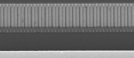
For this study four nominally identical JJ arrays have been fabricated on the same SiO2 isolated silicon substrate. A scanning electron micrograph of such an array is shown in Fig. 1 (c).
The arrays are fabricated using conventional electron beam lithography and shadow-evaporation techniques Dolan (1977); Niemeyer (1974). The shadow pattern is similar to the one described in Ref. Haviland and Delsing, 1996, with the modification that the distance of the SQUID junctions has been extended to about µm for larger flux sensitivity. Between the shadow-evaporation steps an oxide barrier is grown in a pure oxygen atmosphere of 3 Pa for 5 min. The array is connected to a pre-defined wiring layer of an Au-Pd alloy, not shown in the micrograph. The superconducting part of the structure is kept small to reduce influence of non-equilibrium quasiparticles which harm many experiments which rely on the freezing out of quasiparticle excitations at very low temperatures. For a well defined capacitive environment of each island, we put two ground leads at a distance of µm on each side of the array.
The junction capacitance and the coupling capacitance to ground are determined from the geometrical dimensions deduced from scanning electron micrographs. Assuming the value of 45 fF/µm2 for the typical specific capacitance of Al/AlOx/Al tunnel junctionHaviland and Delsing (1996) we estimate the mean self capacitance of the islands to be fF%, where the error margin reflects both systematic deviations as well as island-to-island variations. The capacitance to ground is bounded by aF, by considering the minimal and maximal capacitance of a strip line of similar geometry formed by our ground gate and a center conductor replacing the JJ chain. The screening parameter specifying the number of islands over which the electrostatic potential created by an extra charge drops off is thus bound to
The normal-state resistance of the chain can be derived from the linear slope of the - characteristics at high bias voltage (see Fig. 3 (a)). is the mean resistance across a single SQUID loop. The parameters for the four samples are summarized in Tab. 1. Three of them display very similar parameters while sample I has a much higher resistance. In this paper we focus on measurements for sample III. The results for sample II and IV are very similar. At the end of the paper we briefly point out differences of sample I to sample II–IV.
| Sample | |||||
|---|---|---|---|---|---|
| mV | MΩ | µeV | µeV | ||
| I | 110.0 | 3.13 | 53 | 107 | 0.49 |
| II | 97.3 | 1.32 | 125 | 95 | 1.31 |
| III | 94.5 | 1.46 | 113 | 93 | 1.21 |
| IV | 93.4 | 1.32 | 125 | 92 | 1.37 |
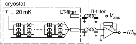
The setup is summarized in Fig. 2. The sample is mounted inside a RF-tight copper box held at the base temperature ( mK) of a commercial dilution refrigerator. All electrical connections of this box are carefully filtered by metal powder filters (cutoff frequency MHz). Together with lumped element filters thermally anchored at the mixing chamber they form low-temperature (LT) filters with a bandwidth of about 10 kHz. All wires leading into the cryostat, which is by itself a metallic cage, are equipped with -filters to keep the interior of the cryostat RF-free. For the - characteristics the current is recorded with a homemade transimpedance amplifier. The output voltage of the amplifier is measured with a digital voltmeter, with a gate time of 200 ms. The voltage drop over the line impedance is accounted for numerically to yield the actual bias on the sample .
(a) (b)
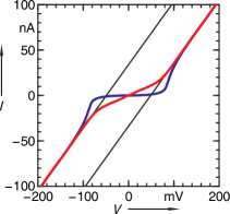
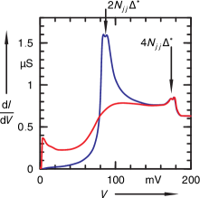
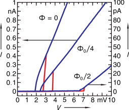
Fig. 3 (a) shows - characteristics on a large bias voltage scale up to mV measured at two different frustrations (red) and (blue). Intermediate magnetic fields interpolate periodically between these curves. The dependence on magnetic field is largest below a voltage threshold which corresponds approximately to mV. The steep rise at zero magnetic field, evident from the blue curve in Fig. 3 (a), can tentatively be identified with the onset of pair breaking processes and the transport above is dominated by quasiparticles. Here, the energy gap can be smaller than the zero temperature gap of aluminum due to non-equilibrium effectsKrasnov (2006).
At lower bias voltages, the charge transport has to rely on the Josephson coupling which is strongly suppressed at . The periodic modulation of the transport characteristics below is evidence that the main transport mechanism in this voltage bias regime is due to the motion of Cooper pairs. However, the motion of Cooper pairs is presumably incoherent as it is accompanied by dissipation. The magnetic field dependence is much weaker at , but still significant. Fig. 3 (b) displays the differential conductance for sample IV. Here the field dependence above is clearly visible. Only above an energy scale set approximately by the field dependence is below the experimental resolution. Sample II and III (data not shown) show a very similar crossover from magnetic field-dependent to magnetic field-independent.
At voltages mV the - characteristics approach approximately straight lines shown in black in Fig. 3 (a). The lines for positive and negative voltages display a horizontal distance of mV. This value is in approximate agreement with µV where has been estimated from the geometry of the contacts. is the most simple estimate of the asymptotic offset voltage due to the Coulomb blockade of single charge transport. According to Fig. 3 (b) the asymptotes at high voltage bias have a slightly lower slope than the estimates based on the intermediate voltage range. The features in Fig. 3 (b) at and have remarkable similarities with stacks of intrinsic Josephson junctions in HTC-cupratesKrasnov (2006). These have been explained by nonlinear non-equilibrium quasiparticle relaxation, which is also reasonable to assume here. The lower slope above can be interpreted as sign of a lower quasiparticle density due to recombination.
For the remaining part of this paper we focus on the properties of - characteristics at much smaller voltages. Fig. 4 gives three examples at different values of the magnetic flux penetrating each SQUID loop. In each case a hysteresis in the - characteristic is found. For other values of the behavior interpolates periodically between the shown examples. At zero voltage bias the differential resistance approaches a value above the measurement limits set mainly by the current resolution (rms) of the setup to G. On increasing the bias the blockade of Cooper pair transport prevails up to a switching voltage , see sharp increase of the conductance colored red in Fig. 4. For higher bias the - dependence follows a (dissipative) straight branch which extends on lowering the bias to voltages below . In the backsweep of the bias voltage the chain retraps in a continuous manner at a well defined ; no discontinuous ”jumps” could be detected.
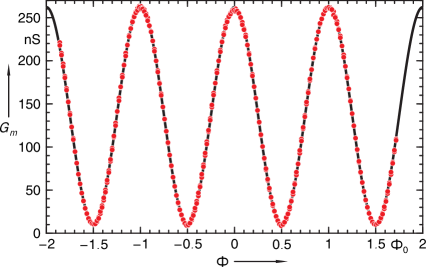
Figure 5 shows the measured slope of the - curves above the switching voltage as a function of the applied flux. In this range the differential conductance is in good approximation independent of the bias voltage (see Fig. 4) and thus gives a measure for the strength of dissipation. In Fig. 5 we underlay a function of the form (black line, nS and nS) to the measured data points.
In comparison with Eq. (1) it is evident that is proportional to . This is our main result. It is rather surprising that the effective Josephson coupling of a single superconducting loop gives already a good description of the dissipative conductance branch of a chain of loops. However, very little is known on the collective effects of the simultaneous transport of cooper pairs and quasiparticle excitations along a chain of small Josephson junctions.
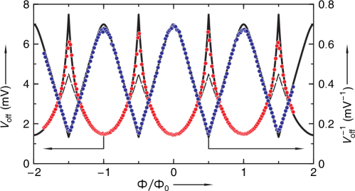
The linear behavior above switching evident from Fig. 4 defines a further voltage at which these straight lines cross the abscissa of zero current. In Fig. 6 we present empirical findings for as a function of the frustration . The measured data (red dots) are well approximated by
| (2) |
A least square fit yields mV, , and mV. This functional dependence is shown as solid line in Fig. 4. Equation (2) expresses the following experimental findings: plotted as a function of (blue dots in Fig. 4) has a hyperbolic shape; it follows a quadratic behaviour in the vicinity of (more generally close to ). On increasing it quickly approaches a straight line with a slope of mV. At maximal frustration (), we find a finite value of about mV and the slope in switches sign.
Figures 5 and 6 display explicit results for sample III. The other, nominally identical samples on the same chip show a very similar behaviour with differences only in small details. For samples II and IV we observe a splitting of the minima in around . Similar effects have been reported by other authors (see, e. g., Ref. Haviland and Delsing, 1996) and can be attributed to typical artefacts of the fabrication method. Sample I displays a similar blockade of current at small bias and a sinusoidal modulation of , too, although is by a factor of 2 smaller as compared to the other samples. However, it lacks the hysteresis observed for the other samples and displayed in Fig. 4 for sample III.
A reliable theory for the system investigated in this paper is still missing. The system is difficult to describe theoretically because the interplay between Cooper pair and quasiparticle tunneling on the one hand—different rules apply in both cases—and the conversion between these distinct species of charge carriers on the other hand. Here, we present a simple phenomenological picture, which is in good agreement with our findings.
The chain of superconducting islands as a whole is voltage biased. The shunt build by the stray capacitance of the leads in parallel to the chip capacitance of the low temperature LP-filters (see Fig. 2) stabilizes the voltage drop across the chain; in case of tunneling, the voltage drop does not change significantly. On the contrary, a current biased setup would require a Thévenin’s equivalent impedance large compared to at the relevant frequencies, which is as high as the plasma frequency of the Josephson junctions GHz. In practise, this requirement is seldom fulfilled because any stray capacitance in the vicinity of he array will result in a low impedance environment at high frequencies.
For junctions deep inside of the array the situation appears different. Its environment can be viewed as a transmission line made from a chain of lumped element units. Each unit contains a Josephson element and and its transmission properties are dominated by the Josephson inductance shorted by to ground. A chain of such units has a typical impedance of for all frequencies below . This argument shows that each junction of the chain is effectively current biased although the device as a whole is connected to a voltage source. Furthermore, to a good approximation individual junctions are embedded into an environment of predominately ohmic impedance at all relevant frequencies.
The situation of a Josephson junction in a resistive environment is well described by -theory Ingold and Nazarov (1992) which yields for the tunneling rate of Cooper pairs:
| (3) |
and
is the probability of the appropriate energy exchange between the tunneling Cooper pair and the electromagnetic environment of the Josephson junction. is an equilibrium phase-phase correlation function which can be expressed via the fluctuation-dissipation theorem as an integral over the real part of the complex impedance , where is the impedance of the environment of the Josephson junction. The essence of Eq. (3) is the proportionality between the incoherent tunneling rate and . It is a direct consequence of Fermi’s golden rule used in the theory to derive Eq. (3). In the present case of , P(E) is expected to peak at : For junctions inside the array tunneling of Cooper pairs has a high probability at a voltage drop of order of . The voltage on each junction is increasing with a rate until a tunneling event at around leads to a sudden jump by . For different junctions in the chain the voltage will be different. The mean voltage will adjust itself in a dynamical manner depending on local details and is increasing proportional to the current due to the incoherent nature of the assumptive process.
In conclusion we have demonstrated that the current in an one-dimensional array of small capacitance Josephson junctions just above the threshold voltage is mainly carried by incoherent tunneling of cooper-pairs and follows a characteristic behavior. This is supported by the -theory, in the situation where one dominating superconducting island is embedded in an high impedance environment of many islands.
References
- Goldman and Markovic (1998) A. M. Goldman and N. Markovic, Physics Today 51, 39 (1998).
- Haviland and Delsing (1996) D. B. Haviland and P. Delsing, Phys. Rev. B 54, R6857 (1996).
- Hermon et al. (1996) Z. Hermon, E. Ben-Jacob, and G. Schon, Phys. Rev. B 54, 1234 (1996).
- Rachel and Shnirman (2009) S. Rachel and A. Shnirman, Phys. Rev. B 80 (2009), 10.1103/PhysRevB.80.180508.
- Homfeld et al. (2011) J. Homfeld, I. Protopopov, S. Rachel, and A. Shnirman, Phys. Rev. B 83 (2011), 10.1103/PhysRevB.83.064517.
- Chow et al. (1998) E. Chow, P. Delsing, and D. B. Haviland, Phys. Rev. Lett. 81, 204 (1998).
- Agren et al. (2001) P. Agren, K. Andersson, and D. B. Haviland, J. Low Temp. Phys. 124, 291 (2001).
- Ambegaokar and Baratoff (1963a) A. Ambegaokar and B. Baratoff, Phys. Rev. Lett. 10, 486 (1963a).
- Ambegaokar and Baratoff (1963b) A. Ambegaokar and B. Baratoff, Phys. Rev. Lett. 11, 104 (1963b).
- Tinkham (1996) M. Tinkham, Introduction to Superconductivity, 2nd ed. (McGraw-Hill, Inc., 1996).
- Dolan (1977) G. Dolan, Appl. Phys. Lett. 31, 337 (1977).
- Niemeyer (1974) J. Niemeyer, PTB-Mitteilungen 84, 251 (1974).
- Krasnov (2006) V. M. Krasnov, Phys. Rev. Lett. 97 (2006), 10.1103/PhysRevLett.97.257003.
- Ingold and Nazarov (1992) G.-L. Ingold and Y. V. Nazarov, “Charge tunneling rates in ultrasmall junctions,” in Single Charge Tunneling – Coulomb Blockade Phenomena in Nanostructures, NATO ASI series. Series B, Physics No. Vol. 294, edited by H. Grabert and M. H. Devoret (Plenum Press, New York, 1992) Chapter 2.