Etching of Cr tips for scanning tunneling microscopy of cleavable oxides
Abstract
We report a detailed three-step roadmap for the fabrication and characterization of bulk Cr tips for spin-polarized scanning tunneling microscopy. Our strategy uniquely circumvents the need for ultra-high vacuum preparation of clean surfaces or films. First, we demonstrate the role of ex-situ electrochemical etch parameters on Cr tip apex geometry, using scanning electron micrographs of over 70 etched tips. Second, we describe the suitability of the in-situ cleaved surface of the layered antiferromagnet La1.4Sr1.6Mn2O7 to evaluate the spin characteristics of the Cr tip, replacing the UHV-prepared test samples that have been used in prior studies. Third, we outline a statistical algorithm that can effectively delineate closely-spaced or irregular cleaved step edges, to maximize the accuracy of step height and spin-polarization measurement.
I Introduction
Spin-polarized scanning tunneling microscopy (SP-STM) is a powerful technique for real-space imaging of atomic-scale spin features. Wiesendanger (2009); Bode (2003) Its implementation, starting from a conventional scanning tunneling microscope (STM) setup, requires careful preparation of (1) a tip with a well-defined magnetic termination and (2) a test sample with nanoscale magnetic structure.
Tips for SP-STM have been fabricated using bulk ferromagnetic (FM) Cavallini and Biscarini (2000); Ceballos et al. (2003) or antiferromagnetic (AF) Shvets et al. (1992); Li Bassi et al. (2007) materials, or by evaporating a thin magnetic film on a nonmagnetic tip. Kubetzka et al. (2002); Rodary et al. (2011) While FM tips afford larger spin contrast, AF tips produce negligible stray fields and are better suited for nondestructive imaging. AF tips etched from bulk Cr are one emerging candidate for SP-STM, ideal for their monatomic composition and high Néel temperature of 311 K. They typically exhibit a canted tip magnetization which is rotatable in a 2 T field, sensitive to all 3D spatial components, and capable of atomic-resolution imaging. Li Bassi et al. (2007); Schlenhoff et al. (2010); Corbetta et al. (2012); Romming et al. (2013); Doi et al. (2015) However, the extent to which the electrochemical preparation influences these characteristics is poorly understood. Systematic studies of tip etching parameters have been mostly limited to nonmagnetic W, whose electrochemistry differs notably from that of Cr. Ibe et al. (1990); Oliva et al. (1996); Bastiman et al. (2010)
A major practical advantage of bulk Cr tips is that they circumvent the need for complex ultra-high vacuum (UHV) cleaning and evaporation procedures, as well as in-situ tip exchange. However, the magnetic samples so far used to quantify spin polarization, e.g. Fe3O4, Shvets et al. (1992) Cr(001), Li Bassi et al. (2007) Fe/W(110), Schlenhoff et al. (2010) and Co/Cu(111) Corbetta et al. (2012), all involve extensive surface preparation in a UHV environment.
Here we report a detailed roadmap for non-UHV Cr tip preparation and evaluation, using three key new strategies. First, we examine how ex-situ fabrication parameters affect Cr tip apex geometry, which in turn influences both atomic- and spin-resolution imaging. We etched more than 70 Cr rods under various voltage sequences, and used a scanning electron microscope (SEM) to image the tips formed on both ends of the break junction. Second, we prepare test samples for tip characterization by mechanical cleaving as opposed to UHV cleaning and evaporation. We use the cuprate Bi2Sr2CaCu2O8+δ to evaluate atomic resolution, and the layered antiferromagnet La1.4Sr1.6Mn2O7 to evaluate spin polarization. Third, we introduce a Gaussian mixture model that can accurately quantify step heights and spin-polarization despite the common challenges of closely-spaced or irregular terraces. Our work charts a path to calibrated spin-polarized tunneling measurements, eliminating the need for UHV surface preparation tools.
II Chromium tips
We etched tips from square 0.5 mm 0.5 mm polycrystalline Cr rods (99.99 purity) 111The square 0.5 mm 0.5 mm rods were cut from polycrystalline Cr foil purchased from Brooks Precision. using the standard direct current (DC) drop-off method. Chen (2007) Figure 1(a) gives a photograph of our setup. One end of the rod was covered with a 7 mm polytetrafluoroethylene (PTFE) tubing Iijima and Yasuda (1988) and immersed in a 5 M NaOH solution, such that the rod area in contact with the solution was minimized. Next, we applied a DC voltage to drive the anodic dissolution of Cr, eventually into CrO4-. The exposed portion of the rod was thinned until the weight below exceeded the tensile force and broke off, leaving behind a work-hardened tip on both ends of the break. The voltage was quickly shut off and both the remnant tip above the break (called top) and the remnant tip below the break (called bottom) were rinsed in deionized water and retained for subsequent examination. We used a fresh solution (poured from the same stock) for each etch in order to standardize our tip preparation.
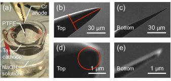
We evaluated the tips using a Zeiss Ultra Plus SEM. Figures 1(b-e) present sample micrographs of two tips derived from the bottom and top rod ends of a single etch, at two different magnifications. We utilized two metrics to assess the tip apex geometry: (1) Aspect ratio (AR), defined as length over width measured 50 m from the tip end (perpendicular lines in Fig. 1(b)), and (2) radius of curvature (RC), computed from a polynomial fit to the tip apex contour (circle in Fig. 1(d)). Our results were robust across different definitions of AR with varying lengths from the tip end.
Figure 2(a) displays the average tip apex AR for etch voltages of 7 V, 11 V and 15 V, binned by top and bottom tips. The bottom Cr tips are statistically sharper than their top counterparts, because they were instantaneously disconnected at the break and did not sustain residual etching in the few seconds before the voltage was manually shut off. Bryant et al. (1987); Iijima and Yasuda (1988); Ceballos et al. (2003) Furthermore, the average ARs are largely uncorrelated with the etch voltage or sequence. No improvements are detected with a two-step process, whereby the voltage was reduced from 9 V to 3 V after a fixed time period (right end of axis break in Fig. 2(a)). Li Bassi et al. (2007) In fact, the two-step process, with its longer etch time typically exceeding 30 minutes, was likely more susceptible to external perturbations (e.g. vibrations or solution evaporation), resulting in larger AR variability and unclear distinction between top and bottom tips. In the one-step processes, we also find the average RC of the bottom tips to be smaller than that of the top tips, but the trend is smaller and lacks the statistical significance seen in the AR.
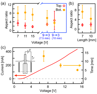
We also considered the effect of the rod weight below the break junction on the tip apex geometry. Ibe et al. (1990) Figure 2(b) presents a comparison between a set of seven Cr rods covered with 7 mm long PTFE tubing and another set of seven covered with 10 mm long tubing, representing a 43 increase in combined weight (rod and tubing). The increased weight yields greater variability in the bottom tip AR despite an average 23 faster etch time, possibly because the larger weight induced an earlier and more uncontrolled break.
To further understand the role of the etch voltage, we obtained a potentiostatic polarization (–) curve for our given setup, shown in Fig. 2(c) (solid line). A minimum of 2 V corresponding to the negative cell potential is required to drive a measurable reaction current. Above this threshold, the current rises approximately linearly with voltage, up to 15 V. Unlike previous reports on W tips, Ibe et al. (1990); Oliva et al. (1996) we do not observe any saturation or upturn in the current that may be indicative of competing or secondary reactions. Figure 2(c) also depicts average etch times (circles) for the voltage settings used in Fig. 2(a), which are faster with increasing current. Taken together, Fig. 2 suggests that for Cr tips, larger voltages may be used to decrease etch times without affecting tip sharpness or inducing additional reactions.
III Scanning Tunneling Microscopy
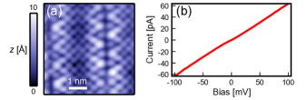
Prior to use for STM imaging, the Cr tips were cleaned by field emission onto a Cr or Au foil within the STM. Typically, we bring the tip into constant-current feedback with a setpoint of 50-100 V and 0.5-3 A for several minutes. This removes any oxides and restructures the terminal atoms on the tip apex, which allows atomic-resolution tunneling largely independent of the post-etch RC. A high post-etch AR, however, is still necessary to ensure a small RC after repeated field emission attempts, and to probe surfaces with large corrugations and step edges. To demonstrate the spatial resolution capabilities of our Cr tips, we used the archetypical cuprate Bi2Sr2CaCu2O8+δ. Figure 3(a) shows a 5 nm 5 nm topographic image of Bi2Sr2CaCu2O8+δ taken with a Cr tip at 7 K. Both the unit cell and the structural supermodulation can be seen. Another purpose of the field emission is to ensure that our Cr tips exhibit flat tunneling conductance on simple metallic Au, as shown in Fig. 3(b). This suggests a featureless tip density of states, consistent with theory. Passoni et al. (2009)
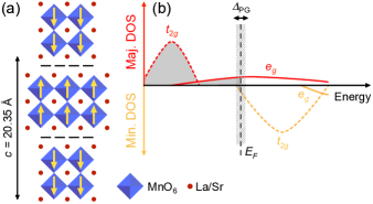
To circumvent the need for UHV preparation of magnetic test sample to evaluate the spin sensitivity of the Cr tip, we propose the use of the cleavable bilayer manganite La2-2xSr1+2xMn2O7. In this material, strong coupling of spin, orbital and lattice degrees of freedom underlies a colossal magnetoresistance effect, Kimura et al. (1996) as well as a diverse display of magnetic orders. Li, Gray, and Mitchell (1999); Mitchell et al. (1999, 2001) Figure 4(a) shows a schematic structure of La2-2xSr1+2xMn2O7 in the Ruddlesden-Popper phase. Sr substitution alters the Mn3+/Mn4+ valency and rapidly changes the magnetic ground state by a delicate tuning of double exchange and crystal field effects. Welp et al. (2001) At = 0.30 (and below 90 K), spins within a given bilayer are aligned parallel to the -axis, but antiparallel to spins in the adjacent bilayers (Fig. 4(a)). Li, Gray, and Mitchell (1999); Mitchell et al. (1999); Welp et al. (2001); Mitchell et al. (2001) If cleavage in the - plane generates step edges spanning adjacent bilayers, then the AF coupling between terraces can be observed using SEM. Konoto et al. (2004) Furthermore, we expect the spin contrast signal to be large due to the approximate half-metallic ferromagnetism within each bilayer. Figure 4(b) shows a schematic diagram of the projected Mn 3 density of states that dominate the La2-2xSr1+2xMn2O7 electronic structure near the Fermi energy. For , the occupied bands within eV of the Fermi energy carry majority spin, Huang et al. (2000) except for a small electron pocket of minority spin character that may be present at the Brillouin zone center. Saniz, Norman, and Freeman (2008); Sun et al. (2013)
In Fig. 5(a), we present a constant-current image of cold-cleaved La1.4Sr1.6Mn2O7, obtained with a Cr tip at 6.5 K. 222The Cr tips used in Figs. 3, 5 were the top halves of rods etched at 10 V for 7 minutes, then at 3 V until the drop-off. These tips were rinsed in deionized water post-etching, but were not SEM-imaged, to avoid possible contamination. We make two remarks. First, due to inferred in-plane screening, STM does not resolve atomic-scale features on the surface of La2-2xSr1+2xMn2O7, save for occasional nanometer-sized patches of square lattice corrugations ascribed to trapped polarons. Rønnow et al. (2006); Santis et al. (2007) It has also been suggested that mobile oxygen defects obscure atomic-resolution tunneling in the layered manganites. Bryant et al. (2011) Second, the cleavage is expected to occur between La/SrO buffer planes (Fig. 4(a)), as deduced from X-ray photoelectron spectroscopy, Loviat et al. (2007) and complemented by other non-spin-polarized STM studies that consistently found step edge heights to be integer multiples of the half-unit cell (/2). Rønnow et al. (2006); Loviat et al. (2007); Massee et al. (2011) Here, multiple terraces are evident over a 60 nm 60 nm area, and we instead observe small variations in their height differences.
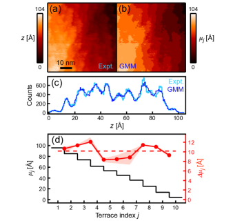
To assess whether these apparent height variations could originate from spin-polarized tunneling, we performed statistical inference with a Gaussian mixture model (GMM), commonly employed in clustering applications. Murphy (2012) The model assumes there are (= 10) underlying terraces, indexed by , each occupying a fraction of the field of view. Within each terrace, the heights are Gaussian-distributed with mean and standard deviation . The objective is to find values of , , and that maximize the (logarithm of the) probability for which the GMM can instantiate the actual data (see supplementary material). This problem can be solved iteratively through the expectation-maximization algorithm. Dempster, Laird, and Rubin (1977) We note the general utility of the GMM approach for STM identification of irregular terrace boundaries by optimization, rather than manual assignment.
Figure 5(b) reveals the underlying terraces inferred from the GMM. Our procedure is validated by the close match of histograms generated from the actual data and the GMM (Fig. 5(c)), which share a Pearson correlation coefficient of = 0.98. The mean terrace heights and their differences are plotted in Fig. 5(d). In the case of bilayer terraces with AF coupling, we expect to exhibit bimodal switching about /2, Wiesendanger et al. (1990) due to a spin-valve contribution to the tunneling current that depends on the cosine of the angle subtended by the tip and sample magnetizations. Here, the height differences may follow a bimodal distribution, but they do not alternate as expected. We enumerate a few possible reasons: (1) A complication could arise from occasional insertions of ferromagnetically-coupled terraces. Although adjacent bilayers have antiparallel spins in the = 0.30 compound, their spins become aligned as soon as the local dopant concentration is raised to = 0.32. Mitchell et al. (1999, 2001) In our case, the nanometer widths of our terraces could be comparable to the length scale of dopant inhomogeneity. We note that the -axis change within , which is around 2%, is too small to explain the observed variations in . Okuda et al. (1999) (2) Previous works have shown that La2-2xSr1+2xMn2O7 crystals in the range can develop a 1-nm-thick layer of nonmagnetic insulator at their surfaces. Freeland et al. (2004). However, spin-polarized SEM measurements with penetration depth 1 nm have detected layered AF texture in the compound. Konoto et al. (2004) (3) Stacking faults can occur during the growth of bilayer crystals, but previous STM studies showed that they were rare and possessed a distinct topographic signal. Massee et al. (2011) Overall, our use of the GMM to extract spin signals is easy to implement and widely applicable, but further measurements, preferably with wider terraces, are needed to fully characterize the magnetic textures of our La1.4Sr1.6Mn2O7 samples and Cr tips.
IV Summary
In summary, we detailed simple approaches to quantitative, atomic-resolution SP-STM that do not require UHV preparation conditions. First, we investigated the preparation of bulk Cr tips by DC drop-off etching. Our findings indicate that the bottom tips are statistically sharper than their top counterparts, and large voltages for faster etches do not reduce tip AR or produce additional reactions. Second, we tested the spatial and spin resolutions of our Cr tips on in-situ-cleaved crystals. We demonstrated atomic-resolution imaging on Bi2Sr2CaCu2O8+δ and flat conductance on Au. More investigation is needed to fully quantify the layered magnetic texture of La1.4Sr1.6Mn2O7; nevertheless, our use of the GMM demonstrates a rigorous framework wherein mean terrace heights can be extracted in the presence of complications such as in-plane screening or possible mobile defects. Our work may aid applications of quantitative SP-STM to cleaved planes of quantum materials that are grown as high-quality single crystals, such as cuprate and Fe-based superconductors, colossal magnetoresistance materials, and topological insulators. Local spin mapping is needed to unravel the exotic electronic behavior of these materials.
V Supplementary Material
See supplementary material for additional images of the etching setup and procedure, a review of the electronic structure of La2-2xSr1+2xMn2O7, details of the Gaussian mixture model used to delineate step edges, and details of the spin-polarization calculation.
VI Acknowledgements
We thank Genda Gu for providing the Bi2Sr2CaCu2O8+δ sample imaged in this work. Work at Harvard was supported by the National Science Foundation under Grant. No. DMR-0847433. D.H. acknowledges support from an NSERC PGS-D fellowship. Work at Argonne National Laboratory (crystal growth and characterization) is supported by the U.S. Department of Energy, Office of Science, Basic Energy Sciences, Materials Science and Engineering Division.
References
- Wiesendanger (2009) R. Wiesendanger, “Spin mapping at the nanoscale and atomic scale,” Rev. Mod. Phys. 81, 1495–1550 (2009).
- Bode (2003) M. Bode, “Spin-polarized scanning tunnelling microscopy,” Rep. Prog. Phys. 66, 523 (2003).
- Cavallini and Biscarini (2000) M. Cavallini and F. Biscarini, “Electrochemically etched nickel tips for spin polarized scanning tunneling microscopy,” Rev. Sci. Instrum. 71, 4457–4460 (2000).
- Ceballos et al. (2003) S. Ceballos, G. Mariotto, S. Murphy, and I. Shvets, “Fabrication of magnetic probes and their application to studies of the (001) surface,” Surf. Sci. 523, 131 – 140 (2003).
- Shvets et al. (1992) I. V. Shvets, R. Wiesendanger, D. Bürgler, G. Tarrach, H. Güntherodt, and J. M. D. Coey, “Progress towards spin-polarized scanning tunneling microscopy,” J. Appl. Phys. 71, 5489–5499 (1992).
- Li Bassi et al. (2007) A. Li Bassi, C. S. Casari, D. Cattaneo, F. Donati, S. Foglio, M. Passoni, C. E. Bottani, P. Biagioni, A. Brambilla, M. Finazzi, F. Ciccacci, and L. Duò, “Bulk tips for scanning tunneling microscopy and spin-polarized scanning tunneling microscopy,” Appl. Phys. Lett. 91, 173120 (2007).
- Kubetzka et al. (2002) A. Kubetzka, M. Bode, O. Pietzsch, and R. Wiesendanger, “Spin-polarized scanning tunneling microscopy with antiferromagnetic probe tips,” Phys. Rev. Lett. 88, 057201 (2002).
- Rodary et al. (2011) G. Rodary, J.-C. Girard, L. Largeau, C. David, O. Mauguin, and Z.-Z. Wang, “Atomic structure of tip apex for spin-polarized scanning tunneling microscopy,” Appl. Phys. Lett. 98, 082505 (2011).
- Schlenhoff et al. (2010) A. Schlenhoff, S. Krause, G. Herzog, and R. Wiesendanger, “Bulk Cr tips with full spatial magnetic sensitivity for spin-polarized scanning tunneling microscopy,” Appl. Phys. Lett. 97, 083104 (2010).
- Corbetta et al. (2012) M. Corbetta, S. Ouazi, J. Borme, Y. Nahas, F. Donati, H. Oka, S. Wedekind, D. Sander, and J. Kirschner, “Magnetic response and spin polarization of bulk tips for in-field spin-polarized scanning tunneling microscopy,” Jpn. J. Appl. Phys. 51, 030208 (2012).
- Romming et al. (2013) N. Romming, C. Hanneken, M. Menzel, J. E. Bickel, B. Wolter, K. von Bergmann, A. Kubetzka, and R. Wiesendanger, “Writing and Deleting Single Magnetic Skyrmions,” Science 341, 636 (2013).
- Doi et al. (2015) K. Doi, E. Minamitani, S. Yamamoto, R. Arafune, Y. Yoshida, S. Watanabe, and Y. Hasegawa, “Electronic and magnetic effects of a stacking fault in cobalt nanoscale islands on the (111) surface,” Phys. Rev. B 92, 064421 (2015).
- Ibe et al. (1990) J. P. Ibe, P. P. Bey, S. L. Brandow, R. A. Brizzolara, N. A. Burnham, D. P. DiLella, K. P. Lee, C. R. K. Marrian, and R. J. Colton, “On the electrochemical etching of tips for scanning tunneling microscopy,” J. Vac. Sci. Technol. A 8, 3570–3575 (1990).
- Oliva et al. (1996) A. I. Oliva, A. Romero G., J. L. Peña, E. Anguiano, and M. Aguilar, “Electrochemical preparation of tungsten tips for a scanning tunneling microscope,” Rev. Sci. Instrum. 67, 1917–1921 (1996).
- Bastiman et al. (2010) F. Bastiman, A. G. Cullis, M. Hopkinson, and K. J. Briston, “Two step optimized process for scanning tunneling microscopy tip fabrication,” J. Vac. Sci. Technol. B 28, 371–375 (2010).
- Note (1) The square 0.5 mm 0.5 mm rods were cut from polycrystalline Cr foil purchased from Brooks Precision.
- Chen (2007) C. Chen, Introduction to Scanning Tunneling Microscopy, 2nd ed. (2007).
- Iijima and Yasuda (1988) T. Iijima and K. Yasuda, “Submicron-scale tip fabrication for magnetic force microscopy by electrolytic polishing,” Jpn. J. Appl. Phys. 27, 1546 (1988).
- Bryant et al. (1987) P. J. Bryant, H. S. Kim, Y. C. Zheng, and R. Yang, “Technique for shaping scanning tunneling microscope tips,” Rev. Sci. Instrum. 58, 1115–1115 (1987).
- Passoni et al. (2009) M. Passoni, F. Donati, A. Li Bassi, C. Casari, and C. Bottani, “Recovery of local density of states using scanning tunneling spectroscopy,” Phys. Rev. B 79, 045404 (2009).
- Kimura et al. (1996) T. Kimura, Y. Tomioka, H. Kuwahara, A. Asamitsu, M. Tamura, and Y. Tokura, “Interplane tunneling magnetoresistance in a layered manganite crystal,” Science 274, 1698–1701 (1996).
- Li, Gray, and Mitchell (1999) Q. Li, K. E. Gray, and J. F. Mitchell, “Spin-independent and spin-dependent conductance anisotropy in layered colossal-magnetoresistive manganite single crystals,” Phys. Rev. B 59, 9357–9361 (1999).
- Mitchell et al. (1999) J. F. Mitchell, J. E. Millburn, M. Medarde, D. N. Argyriou, and J. D. Jorgensen, “Layered manganites: Magnetic structure at extreme doping levels,” J. Appl. Phys. 85, 4352 (1999).
- Mitchell et al. (2001) J. F. Mitchell, D. N. Argyriou, A. Berger, K. E. Gray, R. Osborn, and U. Welp, “Spin, charge, and lattice states in layered magnetoresistive oxides,” J. Phys. Chem. B 105, 10731–10745 (2001).
- Welp et al. (2001) U. Welp, A. Berger, V. K. Vlasko-Vlasov, H. You, K. E. Gray, and J. F. Mitchell, “Effect of layering and doping on the magnetic anisotropy of the layered manganites (=0.3-0.4),” J. Appl. Phys. 89, 6621 (2001).
- Konoto et al. (2004) M. Konoto, T. Kohashi, K. Koike, T. Arima, Y. Kaneko, T. Kimura, and Y. Tokura, “Direct imaging of temperature-dependent layered antiferromagnetism of a magnetic oxide,” Phys. Rev. Lett. 93, 107201 (2004).
- Huang et al. (2000) X. Huang, O. Mryasov, D. Novikov, and A. Freeman, “Electronic and magnetic properties of layered colossal magnetoresistive oxides: ,” Phys. Rev. B 62, 13318–13322 (2000).
- Saniz, Norman, and Freeman (2008) R. Saniz, M. Norman, and A. Freeman, “Orbital mixing and nesting in the bilayer manganites ,” Phys. Rev. Lett. 101, 236402 (2008).
- Sun et al. (2013) Z. Sun, Q. Wang, J. F. Douglas, H. Lin, S. Sahrakorpi, B. Barbiellini, R. S. Markiewicz, A. Bansil, A. V. Fedorov, E. Rotenberg, H. Zheng, J. F. Mitchell, and D. S. Dessau, “Minority-spin states and the degree of spin polarization in ferromagnetic metallic ( = 0.38),” Sci. Rep. 3, 3167 (2013).
- Rønnow et al. (2006) H. M. Rønnow, C. Renner, G. Aeppli, T. Kimura, and Y. Tokura, “Polarons and confinement of electronic motion to two dimensions in a layered manganite.” Nature 440, 1025–8 (2006).
- Loviat et al. (2007) F. Loviat, H. M. Rønnow, C. Renner, G. Aeppli, T. Kimura, and Y. Tokura, “The surface layer of cleaved bilayer manganites,” Nanotechnol. 18, 044020 (2007).
- Massee et al. (2011) F. Massee, S. D. Jong, Y. Huang, W. K. Siu, I. Santoso, A. Mans, A. T. Boothroyd, D. Prabhakaran, R. Follath, A. Varykhalov, L. Patthey, M. Shi, J. B. Goedkoop, and M. S. Golden, “Bilayer manganites reveal polarons in the midst of a metallic breakdown,” Nat. Phys. 7, 978 (2011).
- Note (2) The Cr tips used in Figs. 3, 5 were the top halves of rods etched at 10 V for 7 minutes, then at 3 V until the drop-off. These tips were rinsed in deionized water post-etching, but were not SEM-imaged, to avoid possible contamination.
- Santis et al. (2007) S. Santis, B. Bryant, M. Warner, H. Wang, T. Kimura, Y. Tokura, C. Renner, A. Bianconi, and G. Aeppli, “Imaging of Polarons in Ferromagnetic Bilayered Manganites by Scanning Tunnelling Microscopy,” J. Supercond. Nov. Magn. 20, 531–533 (2007).
- Bryant et al. (2011) B. Bryant, C. Renner, Y. Tokunaga, Y. Tokura, and G. Aeppli, “Imaging oxygen defects and their motion at a manganite surface.” Nat. Commun. 2, 212 (2011).
- Murphy (2012) K. P. Murphy, Machine Learning: A Probabilistic Perspective (The MIT Press, 2012).
- Dempster, Laird, and Rubin (1977) A. P. Dempster, N. M. Laird, and D. B. Rubin, “Maximum likelihood from incomplete data via the algorithm,” J. R. Stat. Soc. Ser. B 39, 1–38 (1977).
- Wiesendanger et al. (1990) R. Wiesendanger, H.-J. Güntherodt, G. Güntherodt, R. J. Gambino, and R. Ruf, “Observation of vacuum tunneling of spin-polarized electrons with the scanning tunneling microscope,” Phys. Rev. Lett. 65, 247–250 (1990).
- Okuda et al. (1999) T. Okuda, T. Kimura, H. Kuwahara, Y. Tomioka, A. Asamitsu, Y. Okimoto, E. Saitoh, and Y. Tokura, “Roles of orbital in magnetoelectronic properties of colossal magnetoresistive manganites,” Mat. Sci. Eng. B 63, 163 – 170 (1999).
- Freeland et al. (2004) J. W. Freeland, K. E. Gray, L. Ozyuzer, P. Berghuis, E. Badica, J. Kavich, H. Zheng, and J. F. Mitchell, “Full bulk spin polarization and intrinsic tunnel barriers at the surface of layered manganites,” Nat. Mater. 4, 62–67 (2004).
- Dessau et al. (1998) D. Dessau, T. Saitoh, C.-H. Park, Z.-X. Shen, P. Villella, N. Hamada, Y. Moritomo, and Y. Tokura, “-dependent electronic structure, a large “ghost” fermi surface, and a pseudogap in a layered magnetoresistive oxide,” Phys. Rev. Lett. 81, 192–195 (1998).
- Mannella et al. (2005) N. Mannella, W. L. Yang, X. J. Zhou, H. Zheng, J. F. Mitchell, J. Zaanen, T. P. Devereaux, N. Nagaosa, Z. Hussain, and Z.-X. Shen, “Nodal quasiparticle in pseudogapped colossal magnetoresistive manganites.” Nature 438, 474–8 (2005).
- Bardeen (1961) J. Bardeen, “Tunnelling from a many-particle point of view,” Phys. Rev. Lett. 6, 57–59 (1961).
- Speight (2007) J. Speight, Lange’s Handbook of Chemistry, 16th ed. (2007).
- Huang (2007) J. Huang, Scanning Probe Microscopy Investigation of Bilayered Manganites, Ph.D. thesis, The University of Texas at Austin (2007).
Supplementary Material
I Etching Setup and Procedure
Figure S1 provides additional photographic documentation of the etching setup and procedure used in this work. In Fig. S1(a), we present a larger scale image of our setup. A support jack raises a 10 mL beaker with 5 M NaOH solution towards a Cr rod, fixed in place by a clamp holder attached to a support stand. We use a set square [pictured in Fig. S1(a)] to ensure that the Cr rod axis is orthogonal to the solution interface. We also carefully cut the polytetrafluoroethylene (PTFE) tubing with a razor blade so that its top end is flat and minimally deformed from a circular cross-section. Its bottom end is pinched to prevent it from slipping off the Cr rod. To drive the etching reaction, we use a DC-regulated power supply (Tenma 72-6628). A 91 resistor placed in series with the circuit stabilizes the etch speed.
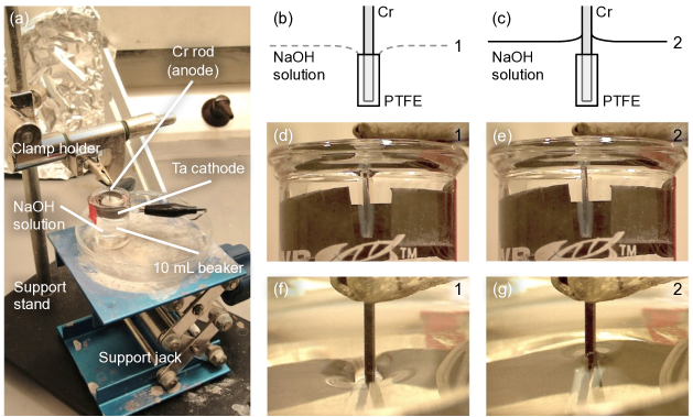
We use a two-step rod immersion procedure to minimize the macroscopic tip aspect ratio, in order to reduce vibrations when scanning. Figures S1(b-g) provide multiple depictions of each step.
II Electronic Structure of La2-2xSr1+2xMn2O7
The schematic electronic band structure of La2-2xSr1+2xMn2O7 presented in Fig. 4(b) of the main text is informed by calculations and experiments in literature. Figures S2(e, f) display the projected Mn 3 density of states (DOS) for the compound, calculated by Huang et al. (2000) Their results indicate that LaSr2Mn2O7 is a half-metallic ferromagnet with a band gap in the minority spin channel of eV. Increasing electron doping (decreasing ) is modeled in the rigid band approximation, resulting in an upward shift of the Fermi level to populate some minority spin states. The rigid band shift is confirmed by angle-resolved photoemission spectroscopy (ARPES) and - calculations for the (Figs. S2(a, b), reproduced from Sun et al. (2013)) and (Figs. S2(c, d), reproduced from Saniz, Norman, and Freeman (2008)) compounds, which predict an electron pocket of minority spin character around the point.
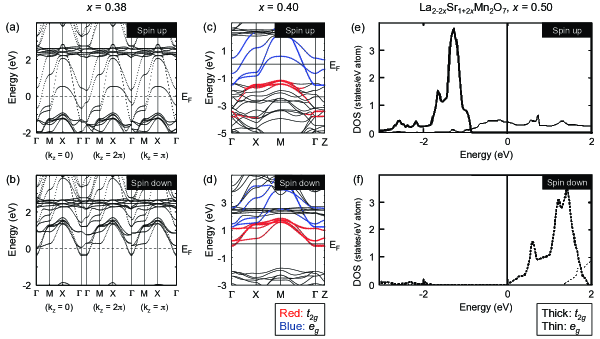
An additional feature in the electronic structure of La2-2xSr1+2xMn2O7 is a “pseudogap” detected by ARPES Dessau et al. (1998); Mannella et al. (2005) and scanning tunneling microscopy (STM). Rønnow et al. (2006); Loviat et al. (2007); Massee et al. (2011) For the compound, STM extracts a gap magnitude of meV by fitting the temperature-dependent zero-bias conductivity to a thermal activation model. Rønnow et al. (2006) Such a pseudogap is not the subject of our discussion, but we indicate its presence in Fig. 4(b) of the main text for completeness.
III Gaussian Mixture Model
We detail our statistical procedure for extracting mean terrace heights from our topographic image of La1.4Sr1.6Mn2O7.
Step 1. Gaussian mixture model (GMM) - For our given topography (Fig. 5(a) of main text), we assume there are (= 10) underlying terraces, indexed by , each occupying a fraction of the field of view. Within each terrace, the heights are Gaussian-distributed with mean and standard deviation .
Step 2. Inference - We determine , , and by maximizing the logarithm of the probability for which the GMM can instantiate our given topography ; Murphy (2012) i.e., we find
| (S1) |
Since Eq. S1 has no closed-form solution, we use the iterative expectation-maximization algorithm Dempster, Laird, and Rubin (1977) to find , , and . Optimal values are given in Table S1.
| [Å] | [Å] | ||
|---|---|---|---|
| 1 | 95.75 0.09 | 2.02 0.06 | 0.01 |
| 2 | 85.08 0.05 | 3.47 0.04 | 0.12 |
| 3 | 73.73 0.05 | 4.21 0.04 | 0.19 |
| 4 | 61.64 0.05 | 3.00 0.05 | 0.10 |
| 5 | 53.28 0.07 | 3.42 0.06 | 0.10 |
| 6 | 44.80 0.04 | 2.28 0.04 | 0.09 |
| 7 | 35.96 0.06 | 4.25 0.05 | 0.19 |
| 8 | 24.54 0.05 | 3.76 0.05 | 0.14 |
| 9 | 13.49 0.04 | 2.04 0.04 | 0.04 |
| 10 | 4.18 0.10 | 2.02 0.08 | 0.01 |
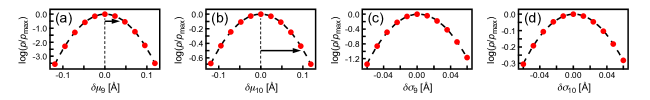
To determine the uncertainties associated with and , we separately vary each parameter while holding the others fixed at their optimal values. In every case, four of which are shown in Fig. S3, the logarithm probability drops quadratically, indicating that the uncertainties are Gaussian. To determine the uncertainties associated with , we additionally require a Lagrange multiplier enforcing . For simplicity, we have not performed this analysis.
Step 3. Background plane subtraction - To correct a small background tilt of our sample relative to the STM tip scanner, we subtract a plane from our topographic image. The and slopes are chosen so to minimize
| (S2) |
the root-mean-square standard deviation across all terraces [Fig. S4].

The uncertainty in resolving the background tilt produces much larger errors in compared to those derived from statistical inference with the GMM (Table S1 and Fig. S3). To assess the errors from the former, we examine values for two sets of tilt corrections that deviate slightly from the optimal background plane (“a” and “c” in Fig. S4 and Table S2). These variations are represented by the faint red background of Fig. 5(d) of the main text.
| ( slope, slope) | a. | b. (0.008, -0.034) | c. |
|---|---|---|---|
| [Å] | 3.623 | 3.619 | 3.802 |
| [Å] | 11.03 | 10.68 | 9.69 |
| [Å] | 11.52 | 11.35 | 11.41 |
| [Å] | 13.01 | 12.08 | 11.93 |
| [Å] | 8.58 | 8.36 | 7.83 |
| [Å] | 9.32 | 8.48 | 7.53 |
| [Å] | 10.23 | 8.84 | 7.34 |
| [Å] | 11.48 | 11.42 | 11.26 |
| [Å] | 11.23 | 11.05 | 10.97 |
| [Å] | 9.66 | 9.31 | 8.96 |
Step 4. Terrace identification - Each pixel has a probability of belonging to terrace , given by
| (S3) |
where is a normalization constant. To produce Fig. 5(b) of the main text, we substitute all the pixels in Fig. 5(a) with the mean height of the terrace with which they are most probably associated.
Step 5. Simulated histogram - To validate our GMM, we simulate a histogram in Fig. 5(c) of the main text, using the optimal values of , , and in Table S1. We draw = 65536 samples, the total number of pixels in our topography. First, we randomly assign each sample to one of the terraces, with probability for terrace . Second, for a pixel assigned to terrace , we randomly determine its height according to a Gaussian probability distribution with mean and standard deviation .
IV Energy-integrated junction polarization
In the case of spin-polarized tunneling between a Cr tip and antiferromagnetic (AF) terraces in La1.4Sr1.6Mn2O7, we expect to exhibit bimodal switching between and , due to a spin-valve contribution to the tunneling current that depends on the cosine of the angle subtended by the tip and sample magnetizations. From these apparent height variations , we can extract an energy-integrated junction polarization .
In the Bardeen formalism, Bardeen (1961) the spin-polarized tunneling conductance (at = 0) is given by
| (S4) |
where is the total density of states of the sample/tip, is the spin-polarized difference, is the angle subtended by the sample and tip magnetizations, is the conductance quantum, and is the matrix element ( is the local barrier height). Chen (2007) Assuming a sample bias of , the spin-polarized tunneling current can be written as
| (S5) |
where is a non-magnetic contribution to the current and
| (S6) |
represents a convolution of the sample and tip magnetizations. In obtaining Eq. S5, we have assumed that and are independent of energy over the range considered.
Next, the tunneling current between a Cr tip and AF terraces in La1.4Sr1.6Mn2O7 is given by when the out-of-plane components of the sample and tip magnetizations are parallel, and when they are antiparallel (here, is the tip magnetization angle relative to the surface normal). In constant-current feedback mode, this translates to a logarithmic increase or decrease in the tip-sample separation , such that . Solving for yields
| (S7) |
where and is approximated by the average of the tip and sample work functions. Wiesendanger et al. (1990)
As a demonstration of this procedure, Fig. S5 shows the theoretical as a function of . Work functions of constituent elements are shown for reference. We take to be the standard deviation of the values in Fig. 5(d) of the main text (also listed in Table S2), but note that does not exhibit the clear bimodal switching expected from spin-polarized tunneling.