Surface bulk differences in a conventional superconductor, ZrB12
Abstract
We studied the electronic structure of a conventional superconductor, ZrB12 using high resolution -photoemission spectroscopy and single crystalline samples. Experimental results with different bulk sensitivity reveals boron deficiency and different valence states of Zr at the surface relative to the bulk. Signature of a satellite features is observed in the Zr core level spectra corresponding to the bulk of the material suggesting importance of electron correlation among the conduction electrons in the bulk while the surface appears to be uncorrelated. These results provide an insight in fabricating devices based on such superconductors.
Superconductors play an important role in technological applications including various medical tools and are potential candidates for future applications such as lossless power transmission, maglev trains etc. Fabrication of devices requires good knowledge of the surface and bulk properties, which are often found to be different in many systems.surface Here, we considered a conventional superconductor, ZrB12; the electronic properties of these systems are well captured by the Bardeen-Cooper-Schriefer (BCS) theory and comes among the simplest cases of the superconducting materials.
ZrB12 exhibits highest superconducting transition temperature ( 6 K) in B12 family Matthias . In the crystal, Zr atoms are surrounded by 24 boron atoms arranged on a truncated octahedron and has the smallest lattice constant (space groupGlaser ; Paderno , = 7.4075 Å) of all known dodecaborides.Fisk Scanning tunneling spectroscopy and magnetization measurements show that ZrB12 single crystal has excellent surface properties.Tsindlekht Enthalpy measurementsStout in Zr0.6Y0.4B12 suggest the most probable valence state of Zr to be (+4). In contrast, the -ray photoemission spectroscopic measurements on polycrystalline ZrB12 sample indicates neutral state of Zr; the earlier observation of (+4) valence state is attributed to the impurity phase. Clearly, the microscopic details of the electronic properties remain to be puzzling and require high resolution studies as observed in other complex systems.Bindu We employed high resolution -photoemission spectroscopy to investigate the electronic structure of single crystalline ZrB12. -rays of varied photon energies in the photoemission spectroscopy reveal interesting differences in the bulk and surface electronic structures.
Single crystals of ZrB12 were grown by floating zone technique as described elsewhere.Geetha The photoemission measurements were performed using a Gammadata Scienta R4000 WAL analyzer and monochromatic Al radiations ( = 1486.6 eV) with the energy resolution set to 400 meV. Hard -ray photoemission (XP) measurements were carried out at P09 beam line, PETRA III Hamburg, Germany with 5947.9 eV () photon energy and an electron analyzer from Specs GmbH with the energy resolution set to 150 meV. The melt grown single crystals were hard and have no cleavage plane. Therefore, we followed surface cleaning procedures such as fracturing using a post on the sample as well as scraping using a diamond file in the vacuum chamber with vacuum better than 310-11 torr. After sample surface preparation in the ultra-high vacuum chamber, it was transported to the experiment chamber without exposing to atmosphere so that the surface remains clean for the photoemission measurements. The angle integrated spectra were found to be reproducible after the surface cleaning cycles and no signature of impurity was found in the spectra. The temperature variation down to 10 K was achieved by an open cycle He cryostat from Advanced Research systems, USA.
The Zr 3 core level spectra were probed using 1486.6 eV (= ) and 5947.9 eV (= ) photon energies. The photoelectron escape depth, (= the distance traveled by the photoelectrons without inelastic scattering) can be varied by varying the incident photon energy.surface The value of of the conduction electrons is close to 20 Å for and about 40 Å for . Assuming at higher kinetic energies (KE), for Zr 3 electrons would be 18.7 Å and 39.5 Å for and , respectively. Thus, at , the photoemission spectrum essentially represents the bulk electronic structure of the sample.
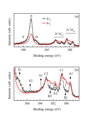
The Zr 3 and B 1 core level spectra collected using and are shown in Fig. 1. At , the B 1 feature exhibit a sharp asymmetric shape as expected in a metallic system. The intensity of the B 1 feature relative to the integrated Zr 4 signal increases significantly at along with an additional feature, D around 187 eV binding energy and increased intensity at higher binding energy side (feature, F). Substantial increase in intensity at the larger probing depth suggests B deficiency at the surface. This effect is found to be independent of the surface preparation consistent with earlier results on single crystal surface cut by diamond saw without chemical etching of the damaged surface layer.Lortz Such boron deficiency at the surface can arise due to the poorer sticking of borons at the top of the huge B12 cages at the surface.
The Zr 3 spectral region (179 - 186 eV) exhibits multiple distinct features denoted by A1, A2, B1, B2, C1 and C2 in the figure - 1’s and 2’s are used for 3 and 3 signals, respectively. The spin-orbit splitting is found to be about 2.3 eV. The intensities of the features changes significantly with the change in surface sensitivity of the technique indicating significantly different surface and bulk electronic structure. At , the intensity of the features, B1 and B2 become almost insignificant although it has large intensity in the spectrum indicating surface nature of these peaks. The features, A1 and A2 reduces in intensity in the bulk sensitive spectrum. Evidently, the bulk electronic structure is dominated by the contributions from the features C1 and C2. Two additional features S1 and S2 are also observed in the spectra - the intensity of these features become stronger in the bulk sensitive spectrum again suggesting their bulk nature.
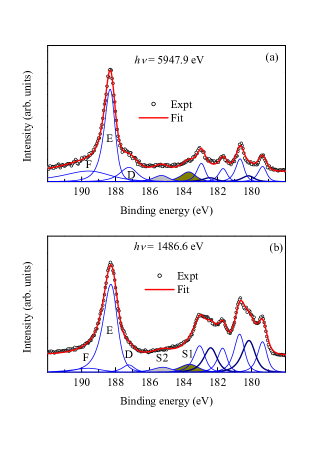
To determine the energy position and relative weight of the spectral features, we have fit the experimental spectra with a set of asymmetric Doniach-Šunjić-type lineshapes,Doniach which is expected in metallic samples due to low energy excitations across in the photoemission final states. Three distinct features in each of the spin-orbit split signals were represented by three peaks as shown in Fig. 2 and the spin-orbit splitting is set at the experimental value of 2.3 eV. The least square error fitting method provides the intensity ratio of the spin orbit split features close to their multiplicity.
The thick solid lines superimposed over the experimental data in Fig. 2 exhibit good representation of the experimental spectra. The binding energies of the features A1 and C1 are found to be 179.4 eV and 180.7 eV - these energies correspond well with the 3 peak positions observed for Zr0 and Zr2+ species, respectively. This is different from the spectra observed from polycrystalline samples containing signature of boron oxides.Flores Such multiple valency of Zr have been observed in Zr halides, oxides,Morant ; Wells ; Sarma and other dodecaborides, YbB12, UB12, etc. as well.Stout ; Takahashi The binding energy of feature B1 is found to be about 180.2 eV, which corresponds to Zr+.
Evidently, the results on ZrB12 reveal unusual mixed valency of Zr - different kinds of mixed valency at the surface and bulk of the sample. The spectrum exhibits distinct signature of the feature ’B’s corresponding to Zr+ species (thick solid lines in the figure) and a larger intensities of the features ’A’s relative to that of ’C’s. This suggests large contributions from Zr0 and Zr+ at the surface while the bulk is dominated by Zr2+ contributions along with Zr0 contributions. Zr+ possessing electronic configuration of [Kr]45 is not a stable configuration and hence is unstable in the bulk. Any such entity would charge disproportionate to Zr0 and Zr2+.cmvarma The boron deficiency at the surface provides a reconstructed electronic structure stabilizing the Zr+ entities.
The features S1 and S2 (see Figs. 1 and 2) exhibit the energy separation close to 2.3 eV, which is similar to the spin-orbit splitting. These features could be fit with two peaks marked S1 and S2 in Fig. 2 and are attributed to the satellite features associated to the photoemission of 3 electrons. The other possibility could be loss features due to various collective excitations in the solid such as plasmon excitations, phonon excitations etc. If that is the case the signature of such loss features would appear with every core level studied and we did not observe this to happen with any of the boron core levels studied. Moreover, the energy separation of such feature in Zr 3 spectra shown in Fig. 3 is much larger than 3 eV observed in the 3 core level spectra. Thus, one can rule out the possibility of loss features in the present case. The intensity of the satellite feature increases with the increase in bulk sensitivity indicating that these are associated to the bulk electronic structure dominated by Zr2+ contributions.
The boron (B 1) core level spectrum also shows an asymmetry towards higher binding energies.Doniach The binding energy of B 1 is consistent with the reported values in typical transition metal boridesPerkins and borocarbides RNi2B2C (R = Y and La)Fujimori (187.1 - 188.3 eV). We have not observed evidence of impurity phases such as B2O3 (B 1; 191.10 eV) in our spectra in contrast to that found earlier in the case of polycrystalline ZrB12 sample.Flores Although, all the boron sites are equivalent from the crystal structure point of view, observation of three distinct features with significantly different binding energies indicate presence of more than one type of B in the crystal. The intensity of the feature at 187 eV (feature D in Fig. 2) is more intense in the relatively more bulk sensitive spectra indicating its bulk nature. These boron atoms presumably reside closure to the Zr2+ sites with largest effective negative potential leading to a lower binding energy.
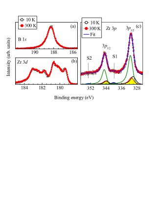
The spectra collected with photon energy at 300 K and 10 K are superimposed in Fig. 3 to see the effect of temperature. Clearly, the line shape of all the core level spectra remain almost identical at these two widely differed temperatures. Although 10 K is little higher than the superconducting transition temperature, the large change in temperature from 300 K to 10 K expected to manifest the phonon induced effects. Almost identical shape and relative intensity of the features in all the core level spectra suggest that the thermal influence on the electronic structure, if there is any, is below the detection level of the technique. In order to investigate the signature of satellite and temperature effects independently on other core level spectra, we analyze the Zr 3 core level spectra in Fig. 3(c). Again, the spectral lineshape is found to be identical at both the temperatures studied. The spectra could be simulated using multiple Zr valencies along with the signature of satellites S1 and S2 associated to the spin-orbit split 3 signals reestablishing independently the observations in the Zr 3 core level spectra.
The atomic number 40 of Zr corresponds to the electronic configuration of [Kr]45. Since, the B12 unit has an effective valency of (2-),Fillipov the expected Zr valency in this system would be Zr2+ with an electronic configuration of 4 - these two electrons will populate the bands leading to the metallic ground state. Since the satellite feature represents the poorly screened feature in the photoemission, the corresponding electronic state configuration will be in the photoemission final state. The main peak, C1 corresponds to the well screened final state, where the positive charge due to the core hole is screened by the transfer of an electron from the conduction band and/or ligands leading to an electronic state ; represent a hole in the ligand levels. The energy separation, of the peak C1 to the satellite feature S1 is about 3 eV. The intensity ratio of the peaks S1 and C1 is in the range of 0.5 to 0.6, which is quite large considering the intensity ratios found in various transition metal oxides such as cuprates.dds Considering the above discussed two final states representing the electronic spectra within the first approximation, the electron correlation strength is expected to be close to 3 eV.dds ; corelevel
In summary, we studied the electronic structure of a BCS superconductor, ZrB12 employing high resolution photoemission spectroscopy. Hard -ray photoemission helped to reveal different surface and bulk electronic structure of this compound. Experimental results exhibit large Zr2+ component in the bulk along with some Zr0 component. Multiple valencies of Zr appear at the surface due to boron deficiency in the surface layers. In addition, we observe signature of satellite feature in the Zr core level spectra indicating finite electron correlation among conduction electrons. Decrease in temperature down to 10 K does not have significant influence in the spectral lineshape and/or energy position indicating the influence from the lattice degrees of freedom is below the detection limit. These results provide evidence of different surface and bulk electronic structure even is a conventional superconductor, ZrB12 that is important to consider while fabricating devices based on these materials.
The authors acknowledge financial support from the DST-DESY project to perform the experiments at P09 beamline at PETRA III, Hamburg, Germany and Dr. Indranil Sarkar for his help during the measurements. The authors, K. M. and N. S. acknowledge the Department of Science and Technology for financial assistance under the Swarnajayanti Fellowship Programme. G.B. wishes to acknowledge financial support from EPSRC, UK (EP/I007210/1).
References
- (1) K. Maiti, U. Manju, S. Ray, P. Mahadevan, I. H. Inoue, C. Carbone, and D. D. Sarma, Phys. Rev.B 73, 052508 (2006); K. Maiti, A. Kumar, D. D. Sarma, E. Weschke, and G. Kaindl, Phys. Rev. B 70, 195112 (2004); K. Maiti, and D. D. Sarma, Phys. Rev. B 61, 2525 (2000); K. Maiti and R. S. Singh, Phys. Rev. B 71, 161102(R) (2005). K. Maiti, R. S. Singh, and V. R. R. Medicherla, Phys. Rev. B 76, 165128 (2007).
- (2) B. T. Matthias, T. H. Geballe, K. Andres, E. Corenzwit, G. W. Hull, and J. P. Maita, Science 159, 530 (1968).
- (3) B. Post and F. W. Glaser, J. Metals Trans. AIME 631, (1952).
- (4) Yu. B. Paderno, A. B. Liashchenko, V. B. Filippov, and A. V. Dukhnenko, Advantages and Challenges in Science for Materials in the Frontier of Centuries, edited by V. V. Skorokhod, (IPMS, Kiev 347 2002).
- (5) Z. Fisk and B. T. Matthias, Science 165, 279 (1969).
- (6) M. I. Tsindlekht, G. I. Leviev, I. Auslin, A. Sharoni, O. Millo, I. Felner, Yu. B. Paderno, V. B. Filipov, and M. A. Belogolovski, Phys. Rev. B 69, 212508 (2004).
- (7) R. W. Mar and N. D. Stout, J. Chem. Phys. 57, 5342 (1972).
- (8) R. Bindu, G. Adhikary, N. Sahadev, N. P. Lalla, and K. Maiti, Phys. Rev. B 84, 052407 (2011); V. R. R. Medicherla, S. Patil, R. S. Singh, and Kalobaran Maiti, Appl. Phys. Lett. 90, 062507 (2007).
- (9) G. Balakrishnan, M. R. Lees, and D. M. K. Paul, J. Crystal Growth 256, 206 (2003).
- (10) R. Lortz, Y. Wang, S. Abe, C. Meingast, Yu. b. Paderno, V. Filipov, and A. Junod, Phys. Rev. B 72, 024547 (2005).
- (11) S. Doniach and M. Súnjic, J. Phys. C: Solid State Phys. 3, 285 (1970).
- (12) L. Huerta, A. Duran, R. Falconi, M. Flores, and R. Escamilla, Physica C 470, 456 (2010).
- (13) C. Morant, J. M. Sanz, L. Galan, L. Soriano, and F. Rueda, Surface Science 218, 331 (1989).
- (14) A. F. Wells, Structural Inorganic Chemistry, edited by A. F. Wells (Clarendon, Oxford, 1975).
- (15) L. Kumar, D. D. Sarma, and S. Krummacher, Appl. Surface Sci 32, 309 (1988).
- (16) F. Iga, Y. Takakuwa, T. Takahashi, M. Kasaya, T. Kasuya, and T. Sagawa, Solid State Commun. 50, 903 (1984).
- (17) C. M. Varma, Phys. Rev. Lett. 61, 2713 (1988).
- (18) C. L. Perkins, R. Singh, M. Trenary, T. Tanaka, and Y. Paderno, Surf. Sci. 470, 215 (2001); S. Patil et al., Solid State Commun. 151, 326 (2011).
- (19) K. Kobayashi, T. Mizokawa, K. Mamiya, A. Sekiyama, A. Fujimori, H. Takagi, H. Eisaki, S. Uchida, R. J. Cava, J. J. Krajewski, and W. F. Jr. Peck, Phys. Rev. B 54, 507 (1996).
- (20) H. Werheit, V. Fillipov, K. Shirai, H. Dekura, N. Shitsevalova, U. Schwarz, and M. Armbruster, J. Phys.:Condens. Matter 23, 065403 (2011).
- (21) D. D. Sarma and S. G. Ovchinnikov, Phys. Rev. B 42, 6817(R) (1990).
- (22) A. E. Bocquet, T. Mizokawa, K. Morikawa, A. Fujimori, S. R. Barman, K. Maiti, D. D. Sarma, Y. Tokura, and M. Onoda, Phys. Rev. B 53, 1161 (1996); K. Maiti, Priya Mahadevan, and D.D. Sarma, Phys Rev B 59, 12457 (1999).