Spin-Resolved Self-Doping Tunes the Intrinsic Half-Metallicity of AlN Nanoribbons
Abstract
We present a first-principles theoretical study of electric field-and strain-controlled intrinsic half-metallic properties of zigzagged aluminium nitride (AlN) nanoribbons. We show that the half-metallic property of AlN ribbons can undergo a transition into fully-metallic or semiconducting behavior with application of an electric field or uniaxial strain. An external transverse electric field induces a full charge screening that renders the material semiconducting. In contrast, as uniaxial strain varies from compressive to tensile, a spin-resolved selective self-doping increases the half-metallic character of the ribbons. The relevant strain-induced changes in electronic properties arise from band structure modifications at the Fermi level as a consequence of a spin-polarized charge transfer between -orbitals of the N and Al edge atoms in a spin-resolved self-doping process. This band structure tunability indicates the possibility ofdesigning magnetic nanoribbons with tunable electronic structure by deriving edge states from elements with sufficiently different localization properties. Finite temperature molecular dynamics reveal a thermally stable half-metallic nanoribbon up to room temperature.
I Introduction
Encouraging theoretical studies and experimental achievements in the preparation and characterization of new materials have increased the scientific efforts to find alternative materials to those used in conventional charge-based electronic devices, optical switches and spin-based electronics [1]. A material exhibiting metallic behavior for electron spins with one orientation and insulating for the spins with the opposite orientation is highly desirable in spintronics. Heusler alloys and compounds based on rare earths are among the prominent half-metallic materials able to conduct electrons in spin-polarized currents [2, 3]. Recently, the versatility in shape and compositions of newly synthesized monolayered materials such as graphene or MoS2 [4] allow us to envision new devices with half- metallic features. External fields have shown promise in tuning the electronic properties of nanoribbons [5], as demonstrated in graphene nanoribbons where half-metallicity may be realized [6]. Also, a scheme based on the oxidation of zigzagged graphene nanoribbons combined with the application of an external electric field allowed for the prediction of half-metallicity in a carbon-based material [7]. In boron nitride, it has been reported that strain fields derived from axial deformation of nanoribbons could reduce the large electronic band gap [8]. These studies offer an interesting opportunity of individually con- trolling the response of the two edges of a nanoribbon to achieve wider tunability of the electronic structure.
Aluminium nitride (AlN) is a large band gap semiconductor with extraordinary physical properties such as small thermal expansion coefficient, high thermal conductivity and a reasonable thermal match to Si and GaAs [9]. AlN also has attractive piezoelectric properties which may be suitable for surface acoustic wave device applications [10]. Balasubramanian et al. provided evidence that tubular AlN structures composed of hexagonal rings of Al and N atoms adopting sp2 hybridization can be fabricated [11]. Zhukovskii et al. reported the structural and electronic properties of single-walled AlN nanotubes of different chiralities and sizes [12]. The successful experimental synthesis and characterization by Xie et al. [13] of pure crystalline AlN nanoribbons with various edge morphologies suggests that controlled growth of desirable architectures based on this group III nitride material may be possible.
In this paper we present theoretical evidence of the tunability of half-metallic and magnetic properties of pristine aluminum nitride nanoribbons by means of both an external applied electric field and longitudinal (axial) strain. A broad spectrum of electronic configurations ranging from a half-metallic to an insulating regime are demonstrated, indicating that purely physically oriented approaches are effective methods to control the electric and magnetic behavior without chemical functionalization or doping. Unlike results reported for graphene [6] and boron nitride [8] nano- structures, but similar to the behavior of ultrathin metal oxide films [14], zigzag pristine AlN nanoribbons exhibit spin-sensitive response to axial strain, yielding a spin-resolved self-doping process that depends on both the spin-configuration of the ribbon and the external stimulus. Fundamentally, we rationalize this tunability as having its origin in the opposing edge states that are derived from orbitals with sufficiently different localization.
II Computational Methodology
The geometry optimizations and electronic structure calculations were performed by means of the SIESTA density functional theory (DFT) based code [15,16]. For each ribbon structure we tested multiple initial magnetic configurations, particularly along the nanoribbon edges, to determine their relative energies. We used a double-polarized basis set within the spin-dependent general gradient approximation (PBE). AlN nanoribbons were modeled within a supercell with at least 10 Å of vacuum to avoid interactions between neighboring cells. Atomic positions were relaxed with a force tolerance of 5 meV/Å. The Brillouin zone integration used a Monkhorst-Pack sampling of 1 1 32 k-points for two-row ribbons. The radial extension of the localized orbitals used a kinetic energy cutoff of 70 meV. The numerical integrals are computed on a real space grid with an equivalent cutoff of 500 Ry.
Selected Perdew-Burke-Ernzerhof (PBE) results from SIESTA were also validated with the plane wave approach VASP [18, 19] to guarantee the robustness of the results. A plane wave cut-off of 400 eV and Brillouin zone sampling identical to the SIESTA calculations was used. Electronic states were occupied using either the Methfesel-Paxton method or Gaussian smearing of up to 0.25 eV. Molecular dynamics simulations were performed in the NVT ensemble for a 4-unit super-cell using only the -point, starting from the ground-state spin-structure for 0% and 8% strain at T = 150 K and T = 300 K. 2.5 ps long runs were performed after an initial equilibration time of 0.8 ps with a 1 fs time-step.
III Results and Discussion
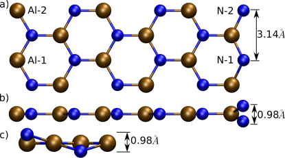
In the following we refer to a bare-edge zigzagged AlN-NR composed of n rows, each with m dimer lines, as [AlN]m(n). The non-passivated dangling sp2 -bonds of the edge atoms are responsible for the unique magnetic and electronic features of the ribbons, so our ribbons are sufficiently wide to avoid interactions between these edge states. Figure 1 shows a schematic representation of a 1.43 nm wide [AlN]6(2) ribbon. A striking characteristic of this nanoribbon is that, in contrast to the Al zigzagged edge that exhibits a flat geometry, N atoms on the opposite edge present a zigzagged ordering above and below the ribbon plane.
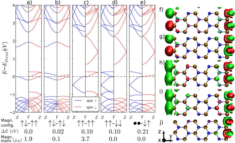
The vertical distance between N edge atoms is 0.98 Å (see Figures. 1(b) and 1(c)). This allows the edge Al-N bond length to be the same as the inner region of the ribbon, namely, 1.81 Å. This bond length is slightly enlarged for bonds at the Al edge. All ribbons considered in this paper are free-standing, as we are interested in understanding their intrinsic properties. Both their geometry and electronic properties could undergo variations depending on a support substrate. We now scrutinize the electronic properties of the [AlN]6(2) ribbon by performing an analysis on the arrangement of five non-equivalent spin configurations shown in Figure 2. Only the - configuration deviates from the initial spin arrangement to end in the - configuration, where signifies zero magnetic moment. A comparison of the energy and the mag- netic moments of each configuration is provided in Figure 2. The ground state corresponds to a system with total magnetic moment of 1.9 and an antiferro- magnetic spin coupling at the Al edge, whereas the opposite N edge exhibits a ferromagnetic coupling between neighboring displaced N atoms (see Figure 2(f)). The highest occupied states (HOS) are below the Fermi level, and the lowest unoccupied state (LUS) of the spin-down channel crosses this limit, yielding a ground state of the [AlN]6(2) ribbon with half-metallic semi-metal features. All other configurations are characterized by different spin at the ribbon edges with a strongly localized character. It is worth noting that flipping the spin of one of the N edge atoms is energetically more expensive than aligning the spins in a ferromagnetic ordering at the Al edge. In this case two energetically equivalent configurations, - and -, are obtained with all spins ferromagnetically coupled along both edges, differing only in their relative orientation across the ribbon width. The electronic band diagram of the - configuration plotted in Figure 2(d) reveals that two electronic states cross the Fermi level for the spin-up channel, but there is a band gap of 2 eV for the spin-down channel. This particular spin arrangement at the edges of the ribbon yields a half-metallic non-magnetic [AlN]6(2) ribbon, 100 meV above the ground state. To gain further insight into the localized character of these magnetic states at the ribbon edges, we performed a projected density of states analysis to determine that the main contributions to the electronic states near the Fermi level comes from the -orbitals of the edge atoms. Specifically, the py and s-orbitals of Al-edged atoms have a large contribution to the HOS whereas the LUS is entirely formed from the py and the px orbitals of the N-edged atoms, with a small contribution from the s-orbitals of the same atoms.
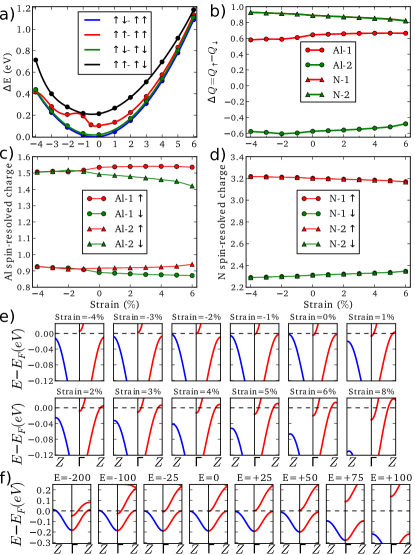
The piezoelectric properties of AlN already motivate its integration with Si integrated circuits [17]. Given the current ability to transfer AlN thin-films onto many different substrates, it is reasonable to explore the possible changes in the electronic and magnetic response to applied strain on AlN nanoribbons. We study the effect of axial deformations on the electronic states and magnetic properties of [AlN]6(2) ribbon. In Figure 3(a) the computed energy vs. strain curves for a [AlN]6(2) ribbon are plotted for the five non- equivalent spin configurations. For each system the energy evolves smoothly, and there is no switching in the energetic ordering of the different spin arrange ments for the considered lattice parameter variation range, from -4% up to 6%, in the z direction (see Figure 2). Only one value of the - configuration diverges from the general quadratic trend exhibited by all configurations upon stretching and compression of the unit cell parameter. Closer examination of the atomic displacements with compressive strain suggests a small barrier to local atomic distortion, similar to isostructural phase transitions in other layered materials [20].
In the band diagrams of Figure 3(e) we show the evolution of the electronic states, near the Fermi level, as a function of the lattice parameter variation fo the most relevant configuration. For compression values of -4% and -3% of the - configuration, the system develops small band gap for both spin channels that renders the [AlN]6(2) ribbon semiconducting. With increasing strain one of the spin channels remains metallic while the HOS of the other spin channel shifts down from the Fermi level, increasing the half- metallicity. The total magnetic moment saturates to 2 . A better understanding of the origin of the half-metallicity enhancement with increasing strain can be obtained from an analysis of the Mulliken population of the edge atoms. The evolution of the charge in each edge atom as a functional of the applied strain is plotted in Figure 3(b), showing the trend of Al edge atoms to gain some charge (N atoms to lose) as the ribbon increases the cell vector. Examining each spin channel separately in Figures 3(c) and 3(d), one notices that a net spin-up charge transfer takes place from the N edge to the Al edge whereas spin-down flows in the opposite direction, from the Al edge to the N edge. The Al to N charge transfer process is visible in the spin-resolved energy band diagrams of Figure 3(e): On increasing the strain starting with a strain of -4%, the spin-down band below Fermi, that is mostly derived from the Al -orbitals, shifts up and crosses the Fermi level as it is emptied. Simultaneously the spin-down band above the Fermi level that is derived mainly from the N -orbitals on the opposite edge shifts down crossing the Fermi level, rendering the system half-metallic. Overall, a net charge migration from the N edge to the opposite Al edge occurs with increasing strain, in a spin-selective self-doping process between the two edges.
The analysis presented above suggests that the magnetic polarization of the ribbon with electronic bands derived from atomic orbitals at opposite edges with sufficiently different electron localization pro perties and with sufficient local spin densities of both channels on the more metallic edge, is the origin of the enhanced half-metallicity. To verify this assumption we have calculated the energy band diagrams of the ground state of a [AlN]6(2) ribbon (-) for different external transversally applied electric fields (i.e., from Al edge to the N edge at positive fields using a sawtooth potential), in order to induce a charge flow that screens the external field across the ribbon width without distinguishing between spins. In Figure 3(f) we plot the spin resolved band structure as a function of a field intensity ranging from E = -200 meV/Å up to E = +100 meV/Å. The general behavior observed for the Al -orbital states is a symmetric response to the external field, decreasing their energy relative to the Fermi level simultaneously for all E. Subsequently, the half-metallicity is barely modified for E values close to 0, and for most of the E values the ribbon exhibits a metallic (from E = -200 up to E = -50 meV/Å) or semiconducting (from E = +50 meV/Å up to E = +100 meV/Å) behavior.
In that perspective, a very appealing strategy to tune the intrinsic half-metallicity of AlN nanoribbons is a combined approach based on the application of an external electric field to a strained ribbon. Our calculations predict that a +4% strained [AlN]6(2) ribbon exhibits enhanced half-metallicity for E = -100 meV/Å, and transitions into a semiconductor for E = +100 meV/Å. Hence, while uniaxial strain allows for the enhancement of half-metallicity by controlling the magnetization density at the Fermi level, anexternal field allows us to reversibly tune the overall electron density at the Fermi level, driving the system either into a metallic or an insulating phase. It is worth pointing out that these transitions are intimately related to the spin arrangement at both edges and that for a spin alignment other than that presented above, the opposite phenomena are observed. We consider now the [AlN]6(2) ribbon with a ferromagnetic spin distribution at both Al and N edges (-). This particular configuration might be obtained by applying a magnetic field perpendicular to the ribbon surface. The metallic state observed in Figure 2(c) remains metallic for an external electric field of E = -100 meV/Å and becomes semiconducting for E = +150 meV/Å. The latter transition is accompanied by an increase of the spin-up charge density at both the Al and N edge atoms, a decrease of the spin-down component at the N edge atoms, and no variation of it on the Al edge atoms. The magnetic moment saturates at 4.0 per unit cell. For the negative value of the applied electric field, spin-up components of both Al and N edge atoms gain some charge, the N edge atom releases some spin-down charge and the corresponding for Al remains the same. The magnetic moment decreases to 3.5 per unit cell. Therefore, unlike the - spin distribution, in the case of the - configuration, uniaxial strain barely affects the electronic bands responsible for the metallic character, and the spin-resolved self-doping is driven by the externally applied electric field. It does not induce half-metallicity due to the symmetric character of the magnetic polarization across the ribbon, but opens a band gap, rendering the ribbon semiconducting.
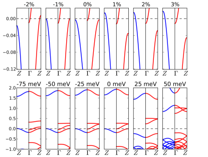
Additional calculations for the [AlN]18(2) ribbons have been conducted to verify that the tunability is conserved for wider ribbons. Indeed by compressing the unit cell down to 2% of the original length the half-metallic character of the nanoribbon is enhanced by lowering of the energy for one of the spin-channel bands. Stretching renders the ribbon metallic, unlike the narrow ribbon that conserved the half-metallic behavior for larger unit cell parameters. The dependency of the electronic properties on the ribbon width clearly suggests the possibilities to explore different conducting or metallic regimes. Finally, applying a ribbon in-plane electric field perpendicular to the axis modifies the [AlN]18(2) ribbon electronic behavior in a similar manner to the [AlN]6(2), namely a band gap develops as the applied field changes from negative to positive values (see Figure 4) .
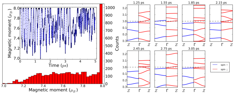
To verify that the half-metallicity and the edge magnetic moments are robust at room temperature, we performed spin-polarized DFT-based molecular dynamics simulations with a Nosé thermostat at T = 300 K on a segment of AlN ribbon 4-unit cell long, i.e., [AlN]6(8) at 0% and 8% strain [18, 19]. The absence of large fluctuations of the total magnetic moment (inset of left panel of Figure 5 for 0%-strain and T = 300 K) is due to the highly localized character of the spins on the ribbon edges and the lack of orbital rearrangement during the ribbon motion, which could otherwise lead to a quenching of magnetic moments. The half-metallicity is robust albeit with temperature dependent fluctuation of the electronic states (see the right panel of Figure 5).
IV Conclusions
We have computed the electronic and magnetic properties of zigzagged bare-edge AlN nanoribbons under external traverse electric field and uniaxial strain.For the ground state, we predict that tensile strain selectively opens a band gap of one spin-channel, enhancing the half-metallicity, while compressive strain yields semiconducting behavior. Depending on strength and direction, transverse electric fields tune the electronic structure from half-metallic to metallic or semiconducting behavior. The applied fields induce a charge polarization across the ribbon with no spin selectivity. In contrast, uniaxial tensile strain induces a selective spin-resolved charge screening which self-dopes the -orbitals of the Al-edge atoms due to a net charge transfer from the opposite N-edge atoms. For certain magnetic states lying energetically close to the ground state, opposite behaviors are found. The ribbon remains half-metallic even at finite temperatures. To our knowledge, this AlN nanoribbon tunability has not been observed or predicted in other nanoribbons and has its origin at edge states derived from orbitals with sufficiently different electron localization.
The presence of opposite local magnetic densities on the Al-edge easily leads to a tunable spin-resolved doping of the more metallic Al-edge from the more localized N-edge states. Since the electronic control is dependent on the effective screening between the two edges in the nanoribbon, increasing the distance between the edges is expected to reduce the tunability of the system under strain. The tunability is significant at least up to a thickness of 18-AlN units in our simulations. The predicted wide tunability of the electronic structure should be independent of the electronic structure theory.
V Acknowledgments
This research used resources of the National Center for Computational Sciences at Oak Ridge National Laboratory (ORNL), under Contract No. DE-AC05- 00OR22725 and the National Energy Research Scientific Computing Center, under Contract No. DE-AC02-05CH11231, both supported by the Office of Science of the U.S. DOE. We acknowledge support from the Center for Nanophase Materials Sciences (CNMS), sponsored at ORNL by the Division of Scientific User Facilities, U.S. Department of Energy.
VI Bibiliography
[1] Wolf, S. A.; Awschalom, D. D.; Buhrman, R. A.; Daughton, J. M.; von Molnár, S.; Roukes, M. L.; Chtchelkanova, A. Y.; Treger, D. M. Spintronics: A spin-based electronics vision for the future. Science 2001, 294, 1488-1495.
[2] Heusler, O. Kristallstruktur und ferromagnetismus der mangan-aluminium-kupferlegierungen. Ann. Phys. 1934, 411, 155-201.
[3] de Groot, R. A.; Mueller, F. M.; vanEngen, P. G.; Buschow, K. H. J. New class of materials: Half-metallic ferromagnets. Phys. Rev. Lett. 1983, 50, 2024-2027.
[4] Dolui, K.; Pemmaraju, C. D.; Sanvito, S. Electric field effects on armchair MoS2 nanoribbons. ACS Nano 2012, 6, 4823-4834.
[5] Du, A. J.; Zhu, Z. H.; Chen, Y.; Lu, G. Q.; Smith, S. C. First principle studies of zigzag AlN nanoribbon. Chem. Phys. Lett. 2009, 469, 183-185.
[6] Son, Y.-W.; Cohen, M. L.; Louie, S. G. Half-metallic graphene nanoribbons. Nature 2006, 444, 347-349.
[7] Hod, O.; Barone, V.; Peralta, J. E.; Scuseria, G. E. Enhanced half-metallicity in edge-oxidized zigzag graphene nanoribbons. Nano Lett. 2007, 7, 2295-2299.
[8] Qi, J. S.; Qian, X. F.; Qi, L.; Feng, J.; Shi, D. N.; Li, J. Strain- engineering of band gaps in piezoelectric boron nitride nanoribbons. Nano Lett. 2012, 12, 1224-1228.
[9] Piazza, G.; Felmetsger, V.; Muralt, P.; Olsson III, R. H.; Ruby, R. Piezoelectric aluminum nitride thin films for microelectromechanical systems. MRS Bull. 2012, 37, 1051- 1061.
[10] O’Leary, S. K.; Foutz, B. E.; Shur, M. S.; Eastman, L. F. Steady-state and transient electron transport within the III-V nitride semiconductors, GaN, AlN, and InN: A review. J. Mater. Sci.: Mater. El. 2006, 17, 87-126.
[11] Balasubramanian, C.; Bellucci, S.; Castrucci, P.; De Crescenzi, M.; Bhoraskar, S. V. Scanning tunneling microscopy observation of coiled aluminum nitride nanotubes. Chem. Phys. Lett. 2004, 383, 188-191.
[12] Zhukovskii, Y. F.; Popov, A. I. Balasubramanian, C.; Bellucci, S. J. Phys.: Condens. Matter 2006, 18, 2045.
[13] Xie, T.; Lin, Y.; Wu, G. S.; Yuan, X. Y.; Jiang, Z.; Ye, C. H.; Meng, G. W.; Zhang, L. D. AlN serrated nanoribbons synthesized by chloride assisted vapor-solid route. Inorg. Chem. Commun. 2004, 7, 545-547.
[14] Moon, E. J.; Rondinelli, J. M.; Prasai, N.; Gray, B. A.; Kareev, M.; Chakhalian, J.; Cohn, J. L. Strain-controlled band engineering and self-doping in ultrathin LaNiO3 films. Phys. Rev. B 2012, 85, 121106-121109.
[15] Ordejón, P.; Artacho, E.; Soler, J. M. Self-consistent order-N densisty-functional calculations for very large systems. Phys. Rev. B 1996, 53, 10441-10444.
[16] Soler, J. M.; Artacho, E.; Gale, J. D.; García, A.; Junquera, J.; Ordejón, P.; Sánchez-Portal, D. The SIESTA method for ab initio order-N materials simulation. J. Phys.: Condens. Matter 2002, 14, 2745-2779.
[17] Clement, M.; Vergara, L.; Sangrador, J.; Iborra, E.; Sanz- Hervás, A. SAW characteristics of AlN films sputtered on silicon substrates. Ultrasonics 2004, 42, 403-407.
[18] Kresse G.; Furthmüller, J. Efficient iterative scheme for ab initio total-energy calculations using a plane-wave basis set. Phys. Rev. B 1996, 54, 11169-11186.
[19] Kresse G.; Joubert, D. From ultrasoft pseudopotentials tothe projector augmented-wave method. Phys. Rev. B 1999, 59, 1758-1775.
[20] Liu, Q. Q.; Yu, X. H.; Wang, X. C.; Deng, Z.; Lv, Y. X.; Zhu, J. L.; Zhang, S. J.; Liu, H. Z.; Yang, W. G.; Wang, L.; et al. Pressure-induced isostructural phase transition and correlation of FeAs coordination with the superconducting properties of 111-type Na1-xFeAs. J. Am. Chem. Soc. 2011, 133, 7892-7896.