J.F.R. Archilla, S.M.M. Coelho, F.D. Auret, C. Nyamhere, V.I. Dubinko and V. Hizhnyakov
Experimental observation of moving intrinsic localized modes in germanium
Abstract
Deep level transient spectroscopy shows that defects created by alpha irradiation of germanium are annealed by low energy plasma ions up to a depth of several thousand lattice units. The plasma ions have energies of 2-8 eV and therefore can deliver energies of the order of a few eV to the germanium atoms. The most abundant defect is identified as the E-center, a complex of the dopant antimony and a vacancy with and annealing energy of 1.3 eV as determined by our measurements. The inductively coupled plasma has a very low density and a very low flux of ions. This implies that the ion impacts are almost isolated both in time and at the surface of the semiconductor. We conclude that energy of the order of an eV is able to travel a large distance in germanium in a localized way and is delivered to the defects effectively. The most likely candidates are vibrational nonlinear wave packets known as intrinsic localized modes, which exist for a limited range of energies. This property is coherent with the fact that more energetic ions are less efficient at producing the annealing effect.
Keywords:
Germanium, ILM, discrete breathers, quodons, defects, DLTS1 Introduction
In science like in many other aspects of human activity, there are often fortunate coincidences that orientate research in unexpected directions. In 2012 there was an international workshop in Pretoria, South Africa, called NEMI 2012 111NEMI 2012: 1st International Workshop: Nonlinear effects in materials under irradiation, March 12-17, 2012, Pretoria, South Africa. P. Selyshev, chairman. Several theoreticians and nonlinear physicists attended, among them there were two of the authors. Several talks were intended for non specialist in order that physics students could be able to understand them. One of the subjects was nonlinear localized excitations that travel along a periodic media without losing energy and keeping their shape. They are called intrinsic localized modes (ILMS) or discrete breathers (DBs). The first name emphasizes the internal character of the phenomenon and reminds us of the linear vibration modes or phonons. The latter name comes from the observation of the internal vibration they experience that can be compared with the breathing of a living being. They were first obtained as an exact solution for the continuous sine-gordon equation germanium-sinegordon . Simulations using molecular dynamics are able to reproduce them in several solids with energies of the order of a few tenths or a few units of an eV.
Among the attendants was a PhD student, part of a research group of the University of Pretoria working on defects in semiconductors, particularly in germanium. They have obtained unexpected results while treating Ge with low energy (2-8 eV) plasma ions. Those energies are known as subthreshold because the threshold energy to produce displacements of atoms in germanium is between 11.5 for the direction and 19.5 eV for the direction germanium-holmstrom2010 . However, they had observed that something was penetrating at least two m inside the germanium wafer and was able to anneal several defects, in particular, the most abundant one, the E-center. The energy for annealing an E-center is about 1.3 eV, according to our measurements and theoretical calculations germanium-tahini2011 . On the other hand the maximum energy that an Ar ion of 4 eV can transmit to a Ge atom is 3.6 eV, therefore the energies were precisely what was expected for ILMs. A line of collaboration was started that joined nonlinear theory, computer simulations, plasma physics and semiconductor physics that eventually confirmed ILMs as the most likely cause of the annealing germanium-archilla-coelho2015 and also suggested them as the explanation for other long-distance effects such as the modification of defects by electron beam deposition, where the energy transmitted was below 1.3 eV germanium-coelho2013 . In this workd we will try to give an explanation of the different branches of the physics involved and to analyze the reasoning that leads to the ILM explanation and the consequences both for semiconductor physics and nonlinear physics.
b]
2 Germanium
t]
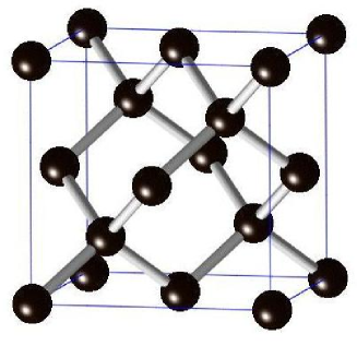
The diamond structure of germanium is well known, each atom has covalent bonds with the four nearest neighbours at the vertices of a tetrahedron as shown if Fig. 1. Normally a conventional cubic unit cell comprised of 8 atoms is used. The diamond structure can be seen as an fcc lattice with two atoms at points and at 1/4 of the diagonal germanium-ashcroft1976 . The lattice unit is Å for Ge, slightly larger than 5.43Å for Si and even larger than 3.57Å for C diamond. The diamond structure is not the best for moving ILMs because there is no chain of nearest neighbours forming a straight line. This is a reason for which, although stationary ILMs have been constructed with molecular dynamics germanium-voulgarakis2004 , the attempts to construct moving ILMs have failed so far. Several lines of research seem promising, one option is to construct ILMs in the next neighbour directions such as where there is a straight line of atoms. Other is to study polarizations as the ones observed for ballistic phonons in germanium or silicon germanium-northrop1980 ; germanium-karamitaheri2013 which can travel distances of 160 nm. It seems also possible that ILMs can be nonlinear perturbations of linear optical modes with high energy, high velocity, short wavelength and low dispersion, such as at the middle of the Brillouin zone for optical branches.
The number of Ge atoms per unit volume can be obtained as . Other properties of interest are atomic number 32, atomic mass amu, density g/cm3, sound velocity m/s, Debye temperature K, Einstein temperature K, covalent radius 1.22 Å, atomic radius 1.52 Å, melting point 1210.55 K, 1st ionization energy 7.899 eV and specific heat 0.32 J/gK at 300 K.
3 Phonons in Ge
The objective of this subsection is to review the well known concepts of lattice dynamics and to see how they apply to Ge and to justify subsequent calculations. Phonons are the usual means for energy transport in a crystal and the responsible party for thermal annealing of defects. With this review we want to demonstrate that they cannot be th responsible for the annealing of the E-center defect during Ar plasma bombardment. We will frequently use general concepts of lattice dynamics and the reader can consult any textbook, for example Refs. germanium-ashcroft1976 ; germanium-dove .
In classical mechanics for a crystal with per unit volume, there are degrees of freedom. In the harmonic approximation the substitution of in the equation of movement leads to different linear modes of frequency , wave number , phase velocity and polarization . They are organized in branches , three of them are acoustic, that is vanishes linearly with in the long wavelength limit. If the crystal has a basis of atoms or ions in each primitive cell, there are also optical branches, that are bounded from below. In Ge with two Ge atoms in the unit cell, there are three optical branches. Each branch has modes. In the classical description, each mode can have any energy with a probability at temperature given by Maxwell-Boltzmann equation , which leads to an average energy that is identical for each mode. Therefore, it is trivial to obtain the energy per unit volume and the specific heat at constant volume , a result known as the Dulong-Petit law. This result is approximate at room temperatures and above but fails spectacularly at lower temperatures, which led to the quantum description of the harmonic crystal. The classical description of the linear modes of the crystal remains valid but the statistics are quite different.
In quantum mechanics a linear oscillator with frequency can only have energies given by , where is the excitation or occupation number. As the ground state energy cannot be lost we will usually suppress it and use
| (1) |
where is the quantum of energy, also called the energy level.
At a given temperature , the average values and can be obtained with Bose-Einstein statistics. They are
| (2) |
where eV/K is the Boltzmann constant.
In a solid with degrees of freedom and therefore the same number of linear modes, each one is equivalent to a linear oscillator with a given frequency . It is usual to describe them as phonons or quasi-particles and to use the expression phonons of a particular type with energy instead of a linear mode or state with frequency and excitation number . We will also follow this convention although in some instances it may be more convenient to revert to the original terminology.
As the number of frequencies is very large and they are very close, and are considered as quasi-continuous variables. Most energy levels are degenerate, i.e., there is more than one mode with that energy, and in the quasi-continuous description there are very many in an interval .
A variable density of states (DOS) is introduced, also some times called the density of levels. It is defined such as is the number of linear modes or quantum phonon states per unit volume with energies between and . For a discrete system the phonon spectrum is always bounded from above, that is, there is a maximum frequency and energy and , therefore
| (3) |
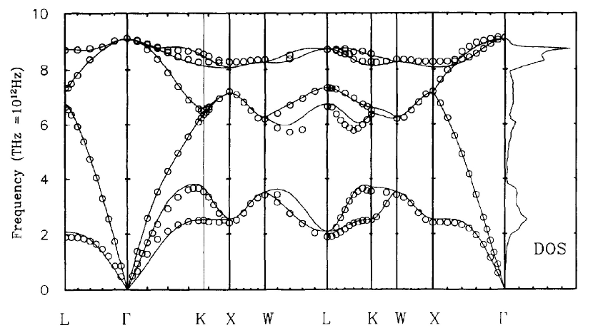
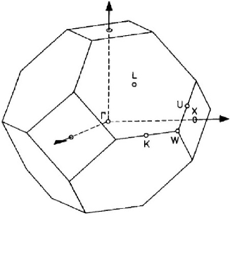
A rough estimate of the maximum value of energy level for the acoustic modes can be obtained using the fact that the minimum value of the wavelength is twice the lattice unit of the primitive cell , then , with the speed for the mode. For Ge, Å and using m/s, we obtain meV and THz similar at the observed values in Figs. 2 and 4. However, such a simple estimate for the optical modes is not possible because the phase velocity tends to infinity when .
Generally speaking there is no minimum frequency or energy as explained above, however, when considering only a part of the system, it can be described as subjected to an external potential representing the interaction with the rest of the crystal. In this case the phonon spectrum becomes optical, i.e., bounded from below.
The energy of the solid per unit volume is given by
| (4) |
We will also use the number density or normalized density of states , with the property that as is the fraction of modes with energies between and and therefore the normalization condition and average phonon energy are given by
| (5) |
There are two approximations frequently used for the density of states: the Debye and the Einstein models. In the Debye model, all phonon modes are substituted by three acoustic branches with dispersion relation , with the same , which is an average velocity. These acoustic branches lead to a density of modes or states per unit volume germanium-ashcroft1976 . Then, , with the constant depending on the particular solid through and . The energy has a cutoff value such that the condition of normalization is fulfilled. Therefore, . The values and are known as the Debye energy and temperature, respectively. Therefore there is only one unknown, either or , either of which cannot be measured as they do not correspond to real magnitudes. What is done is to choose such that the specific heat fits the measurements. For Ge, a value of or meV is usually given, which corresponds to m/s. This velocity is not a real quantity but coherently it is approximately the mean of the velocities of the two transversal modes, m/s, and the longitudinal one, 5400 m/s germanium-lacroix2005 . The Debye dispersion relation works, of course, better for the acoustic branches and small wave vectors.
The Einstein model supposes that there are modes with the same frequency , being and , the Einstein energy and temperature, respectively. The value of is chosen so as to fit the specific heat of the solid, being an average energy of the phonons in the crystal. For germanium its value is K and will be used in this work. In this model the mean energy per unit volume at temperature in germanium is simply
| (6) |
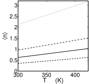
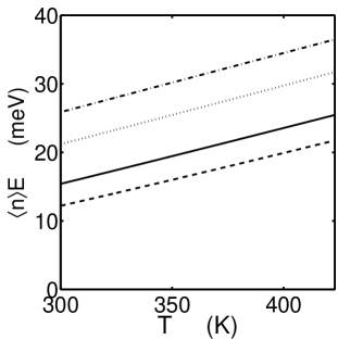
The actual phonon dispersion relation and the density of states have been obtained and checked with experimental ones in Ref. germanium-wei1994 . Both magnitudes are shown in Fig. 2. The normalized density of states can be obtained from it but as the resolution is poor for low energies we have substituted that part by the Debye one. The Ge density of states is shown in Fig. 4 together with the corresponding one for the Debye and Einstein model for comparison. For two concentrations of states appear near the top and near the bottom of the spectrum, with a drastic simplification we can describe them as an optical band around meV and an acoustic one around meV. The mean phonon energy is approximately equal to the Einstein energy.
Figure 5 represents the number of phonons and the average energies as a function of temperature for acoustic phonons, optical phonons, Einstein phonons, and average values obtained with the density of states . It can be seen that the classical statistics is not valid at the temperatures of interest in this work and that there are significant differences between optical and acoustic phonons. The energy in the acoustic modes is larger than in the optical ones in spite of having less energy but with more phonons. It can also be seen that the average number of phonons is smaller or closer to one which indicates that the classical description is not good at room temperatures and above.
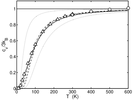
Figure 6 represents the specific heat at constant volume obtained from these models. There is no significant difference at the temperatures of interest in this work between room temperature K and the annealing temperature of the E-center K. This justifies the use of the Einstein density of states as a good approximation for calculations. The specific heats for two Einstein models with and are also represented for comparison.
4 Defects and their detection with DLTS
Point defects in the structure or the type of atoms of the semiconductor can appear with some probability due to the temperature but they can also be created by radiation. In the experiments described in this work most of the defects are created by 5 MeV alpha radiation germanium-kolkovsky2007 ; germanium-roro2009 produced in the decay of the americium isotope 241Am. A Ge sample with dimensions mm is brought into contact with americium foil for 30 minutes.
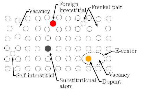
Defects can be of many types, some simple examples are shown in Fig. 7, such as a vacancy, a substitutional atom, a self-interstitial, a foreign interstitial, a Frenkel pair that is, a combination of a vacancy and a self-interstitial and an E-center, which is a combination of a dopant substitutional atom and a vacancy. The germanium sample used in this work is doped with antimony (Sb), with a dopant concentration . Dopant atoms as Sb atoms occupy substitutional positions but are not considered defects as they are an essential part of the semiconductor electrical properties. The main defect appearing after irradiation is the E-center already described. There are many others types such as vacancy complexes like the di-vacancy (V-V), the tri-vacancy (V3), the tetra-vacancy (V4) and combinations of interstitials as di or tri-interstitials (I2, I3). Also, hydrogen (H), due to its small size is able to penetrate almost everywhere and can combine with other defects forming complexes such as VHn, where n is an integer with values from . A variant of the E-center is the A-center, a complex of an oxygen interstitial and a vacancy.
Defects can experience many processes like diffusion, interaction between them, modification, annealing and others. Generally speaking all these processes are enhanced by temperature and the rate at which the process takes place depends in an Arrhenius form on a quantity known as the enthalpy for the process or sometimes referred to as the activation energy or barrier energy for the process. That is
| (7) |
The semiconductor Ge has a band gap of eV. Some defects introduce electrical levels inside the band of a semiconductor, as for example in Sb-doped Ge, Sb introduce levels very close to the conduction band. When they are within the band gap and more than 0.1 eV from the conduction or the valence bands they are considered deep. Usually they are called electron traps when they introduce an electron level and hole traps when they introduce a hole level, respectively. We will write only about electron traps for simplicity, because the treatment of holes is very similar, and because the main defect we are interested in, the E-center, is an electron trap. The E-center is located at eV below the conduction band. The same defect has also been reported as .
When an electron is in a trap level it has a mean time of permanence and its inverse is the probability of emission per unit time. This magnitude and its dependence on temperature are key to defect detection as it is the actual magnitude measured in DLTS germanium-Lang1974 ; germanium-schroder2006 . This dependence can be easily deduced.
Suppose that there are traps per unit volume, the probability for an electron occupying the trap level of energy (not which is ) is given by the Fermi-Dirac distribution
| (8) |
where , the Fermi energy is located near the middle of the phonon band.
The probability that a moving electron is captured by a trap is given by , where is the capture cross section of an electron for the trap, is the thermal velocity of the electrons, the trap concentration, the probability of the trap being empty and the number of electrons per unit volume. The latter quantity can be obtained as , where is the bottom energy of the conduction band, being the effective mass of an electron and is the effective density of states in the conduction band germanium-ashcroft1976 . The thermal velocity can also be obtained as , with .
The trap emission rate is given by , that is, the concentration of traps multiplied by the probability of being occupied and the probability of emission per unit time for a trap. At thermal equilibrium and can be isolated as
| (9) |
with , that is, the distance of the trap level to the conduction band.
It is easy to check that the pre-exponential factor is proportional to as the effective mass is approximately constant at the bottom of the conduction band where most of the occupied states are.
Some authors discuss the interpretation of this expression of the emission rate germanium-dimitrijev2009 as a function of the capture parameters, however and are considered the defect signature and used worldwide. Independently of the meaning has the right dependence on the temperature and should simply considered simply as a parameter of the defect.
The technique known as DLTS, deep level transient spectroscopy, uses a pn junction or a metal-semiconductor junction known as a Schottky diode. A voltage pulse is sent through the junction in reverse bias, so as to flood all the traps with electrons, which after the pulse start to emit electrons towards the conduction band at a rate given by Eq. (9). The capacitance of the junction depends on the charge accumulated in the traps and therefore changes with time as the traps become depleted. It is measured at two different times and . If is the capacitance at and the change in the capacitance between and , it can be demonstrated that the relative change in the capacitance has a maximum when the so called rate window equals the emission probability:
| (10) |
Typical rate windows are 80 s-1 and 200 s-1. Measurements of the DLTS signal are performed while the temperature is changed. When the RW equals the emission rate of some defect a peak appears in the plot of with respect to T. In this way the different defects appear. At the peak
| (11) |
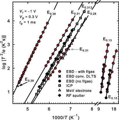
where is the number of dopants in an n-type semiconductor and is the number of traps corresponding to the peak. Using several RWs, several values of can be obtained for different temperatures, being the slope of the representation with respect to . From the same representation the value of can be obtained and therefore the defect is fully characterized. From the height of the peak the concentration of the defect can also be obtained. The value of the reverse bias determines the depth of the measurements and allows for the plotting of the profile of as a function of the depth of the sample. This procedure to characterize the E-center in Ge was performed in Ref. germanium-coelho2013 and the Arrhenius plots for several defects can be seen in Fig. 8.
t]
5 Experiment of plasma-induced annealing
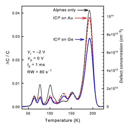
The main experiment is done as follows: (a) The Ge wafer is bombarded with 5 MeV alpha particles during 30 minutes and it is left for 24 hours at room temperature for the defects to stabilize as initially there is a fast kinetic germanium-fagepedersen2000 ; (b) The surface of Ge is divided into two parts and , then a diode is made using resistive evaporation of Au on part and DTLS is performed to measure the defect concentrations, (c) The Ge sample is introduced into an inductively coupled plasma (ICP) with 4 eV Ar ions and pressure of 0.1 mb for half an hour in intervals of 10 minutes to allow for cooling; (d) DTLS is performed in part , where ICP has been done through Au, (e) A diode is evaporated on part , where ICP has been applied directly on the Ge surface, and then, DTLS is performed there.
The short time of alpha irradiation is done to allow for better DLTS measurements. A concentration of about 10% of , as the was obtained, or less is ideal
The results of the three measurements are presented in Fig. 9. We will concentrate on the most abundant defect, the E-center. (1) The concentration after alpha damage and 24 hours rest is ; (2) After direct ICP on germanium it is reduced by 30%; (3) If the ICP is applied through the Au contact, the reduction is about 7%, smaller but still significant.
Other details of interest are: (4) The sample heats up to about 40∘C in spite of the cooling intervals; (5) If there is no cooling the sample heats up to about 65∘C and the decrease in the rate of annealing is dramatic; (6) The defects are annealed up to a depth of 2600 nm inside the Ge sample germanium-archilla-coelho2015 ; (7) If other metals are used for the contact the annealing also takes place as with Au but the effect depends on the metal used; (8) If a plasma of larger energy 8 eV is used the annealing rate increases, but given that a plasma of larger energy also has a larger flux, the effect per Ar ion is much smaller (see below); (9) The temperature to achieve a similar rate of annealing is 150∘C as deduced in Sect. 7 and by other authors germanium-markevich2004 .
There was no measurable concentration of Ar after ICP which discards Ar channelling. Other explanations were considered and discarded in Ref. germanium-archilla-coelho2015 such as multivacancy production, production of minority charge carriers, production of defects that could diffuse and interact with the E-center and diffusion of H that could passivate the vacancies in the E-center.
6 ILM hypothesis
In this section we analyze the experiment and examine the possibility that Ar ions produce intrinsic localized modes that travel in a localized way with little dispersion through the semiconductor and are able to anneal the defects. The exact nature of these ILMs is not yet known but here it is assumed that they have a vibrational part due to their origin from an Ar ion hit. If they have also some charge or other properties is unknown and not necessary for this hypothesis.
The rate of ion-induced annealing is given by the following equation:
| (12) |
where is an effective cross-section for defect annealing by plasma ions. It is as if imaginary Ar ions would penetrate Ge and anneal a defect but at this stage there is no need of an hypothesis, is just the probability per unit time and unit flux of Ar ions that a defect is annealed. Integrating the equation above we obtain:
| (13) |
For the experiment described with pressure mb, that corresponds to 4 eV ions, the flux is germanium-archilla-coelho2015 , s and , and Å2 is obtained. This value should be compared with Å2, that is, the average area corresponding to an atom of Ge at the surface of the semiconductor, then . This result indicates that the process has an enormous efficiency. It has to be considered with caution as also neutrals may be arriving at the semiconductor surface, but it should not change the result by more than one order of magnitude, probably by around a factor of two in the flux.
It is interesting to see what the change in efficiency is when an 8 eV plasma is used. The flux in this case is germanium-archilla-coelho2015 and using only 600 s time the concentration is reduced to 80% of the original. The cross section becomes Å. Therefore a larger energy per Ar ion does not increase the efficiency of the ion-annealing process but reduces it by a factor of . This is coherent with our hypothesis that the Ar+ impacts produce ILMs, because ILMs have a definite range of energies. More energy than what is required will be dispersed into phonons which would interfere with the propagation of the ILMs. It is also interesting to be aware of a few magnitudes to appreciate what could be happening in the semiconductor. Suppose that ILMs travel at a speed of the order of magnitude of the speed of sound in Ge, m/s, the time needed for an ILM to travel the measured depth nm is ns. This means that the area for an Ar+ hit in is a circle with a radius of about lattice units, or in other words each impact and travel is completely isolated.
Note also that the traps are almost isolated as Å or 370 lattice units. Therefore there is no influence between them.
Let us introduce a couple of parameters, the efficiency of ILM creation by Ar ions, that is
| (14) |
and the cross section for ILM defect annealing measured in units, that is
| (15) |
Therefore
| (16) |
and . The cross section should be larger than because the size of an E-center is at least two atoms and due to the complex nature of Ge, ILMs probably have also a complex structure with a few atoms involved perpendicular to the movement of the ILMs. If the interaction takes place at a distance of four atoms then and . The latter result implies that about 20 Ar+ hits are necessary to produce an ILM. The number of Ar+ to anneal a defect can also be calculated easily as .
In the following section it will be made clear that this rate of annealing cannot be produced only by the increase in temperature. Therefore, although the numbers are approximate and many objections can be made there are a few clear consequences of this analysis: (1) Some entity which we call ILM, and most likely it is a vibrational entity, is able to travel distances of a few micrometers inside Ge in a localized way and without losing much energy (2) There is a high efficiency in the conversion of Ar+ hits to ILMs; (3) There is a high efficiency for ILMs to anneal or modify defects.
Note that if the annealing barrier is it is neither necessary for an ILM to have nor to deliver to anneal the defect. The change of the barrier due to the passing of an ILM nearby brings about a change in the annealing rate which can be very high. See Refs. germanium-dubinko2011 ; germanium-dubinko2013 ; germanium-coelhoarchillaquodons2015 ; germanium-dubinkoarchillaquodons2015 .
7 Thermal annealing
In this section we review thermal annealing and apply it to Ge in order to compare the temperature and energy needed to obtain the same rate of thermal annealing as with Ar ions.
Thermal annealing of defects in semiconductors is given by a first order kinetic
| (17) |
where , known as the reaction rate constant is given by an Arrhenius type law
| (18) |
where is known as the annealing energy and as the pre-exponential factor. can be interpreted as the potential barrier which is necessary to surmount in order that the transformation or diffusion process for annealing takes place. The exponential term can be seen as the probability for an accumulation of energy of magnitude . The pre-exponential term has units of frequency and it is also known as the frequency factor. It is related to the number of attempts per unit time that the system tries to pass the barrier and with the curvature of the energy with respect to the reaction coordinate. may also depend on the temperature but in a much weaker way than the exponential term. It also depends on the entropy change.
(a) (b)
(c)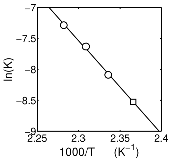
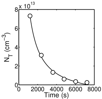
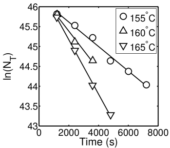
The integration of Eq. (17) leads to the exponential decay and comparing the experimental data with it is possible to obtain . Several data for E-center annealing have been published germanium-fagepedersen2000 ; germanium-markevich2004 . Here we will use the results obtained by some of the authors according to the procedure described in Ref. germanium-nyamhere2009 and using the same dopant and defect concentration as in this work. Figure 10(a) shows the exponential decay at 165∘C and Figure 10(b) represents with respect to time for three temperatures. The approximate linear dependence can be seen. From the slopes, three values of the reaction rate constant are obtained and in Fig. 10(c) is represented with respect to and the linear dependence can be observed. Comparing with the values and eV are obtained. These numbers should be treated with caution as the experimental procedure is very sensitive to the details of the experimental technique. The sample has to be cooled and reheated to measure the defect concentration.
8 Comparison of thermal and plasma-induced annealing
Comparing the equations for thermal annealing Eq. (17) and ion-induced annealing Eq. (12) we can observe that if both process have the same rate of annealing
| (19) |
From this equation, the value of K is obtained.
The thermal energy at per unit volume using Ge density of states from Sect. 3 is given by
| (20) |
Note that the use of the Einstein model with K leads to very similar results. The increment in energy from room temperature K to K is given by
| (21) |
The energy per unit volume of energy in ILMs is given by
| (22) |
where is the density per unit volume of ILMs and is the mean ILM energy. Both quantities are unknown but we can estimate both. The maximum flux of ILMs is the flux of ions and the maximum energy is the energy that a 4 eV Ar ion can deliver to a Ge atom, 3.6 eV. Let us suppose eV and . The velocity of ILMs should be of the order of magnitude of the d velocity of sound, m/s. Then and the ILM energy per Ge atom is
| (23) |
This value is so small because there is only an ILM for every Ge atoms. Therefore the ratio , which proves that an enormously larger amount of energy in phonons is needed in order to produce the same annealing effect than the Ar ions produced. Changes in the ILM energy, their speed, the number of them created by neutrals in the plasma and other factors cannot change their energy density by a factor of .
9 Summary
In this work we have described an experiment in which a low energy, low flux Ar plasma anneals defects in Sb-doped Ge up to a significant depth below the surface. The hypothesis advanced in Ref. germanium-archilla-coelho2015 and continued here is that Ar ions produce some kind of travelling localized excitation with great efficiency. We call these entities intrinsic localized modes or ILMs because their energy and other properties indicates that their energy is vibrational, although this is by no means demonstrated. Some space has been dedicated to phonons in germanium in order to have a clear picture of them and their energies and so doing clarify that they cannot be responsible for the annealing effect, because the ILM energy density is much smaller than the phonon density which produces the same annealing rate. Also we think that the study of the dispersion relation can bring home ideas about how to construct ILMs in Ge, which will be the confirmation of the present hypothesis but seems to be a daunting challenge.
The numbers are approximate, many hypotheses and estimations that have been advanced may be incorrect, however none of these problems can change the fact of the observation of long-range annealing in germanium produced by Ar plasma and that ILMs are the most promising cause.
Acknowledgments
The authors were funded by MICINN, project FIS2008-04848; the South African National Research Foundation and the European Regional Development Fund, Centre of Excellence Mesosystems: Theory and Applications. JFRA and VD acknowledges the Physics Institute in Tartu for their hospitality.
References
- (1) Archilla, J.F.R., Coelho, S.M.M., Auret, F.D., Dubinko, V.I., Hizhnyakov, V.: Long range annealing of defects in germanium by low energy plasma ions. Physica D 297, 56–61 (2015)
- (2) Ashcroft, N.W., Mermin, N.D.: Solid State physics. Saunders College Publishing, Philadelphia (1976)
- (3) Berger, L.I.: Semiconductor Materials. CRC Press, London, UK (1996)
- (4) Coelho, S.M.M., Archilla, J.F.R., Auret, F.D., Nel, J.M.: The origin of defects induced in ultra-pure germanium by electron beam deposition. In: J.F.R. Archilla, N. Jiménez, V.J. Sánchez-Morcillo, L.M. García-Raffi (eds.) Quodons in mica: nonlinear localized travelling excitations in crystals. Springer (2015). To appear
- (5) Coelho, S.M.M., Auret, F.D., Janse van Rensburg, P.J., Nel, J.: Electrical characterization of defects introduced in n-Ge during electron beam deposition or exposure. J. Appl. Phys. 114(17), 173,708 (2013)
- (6) Dimitrijev, S.: Irreversible event-based model for thermal emission of electrons from isolated traps. J. Appl. Phys. 105, 103,706 (2009)
- (7) Dove, M.T.: Introduction to lattice dynamics. Cambridge University Press, Cambridge, UK (2005)
- (8) Dubinko, V.I., Archilla, J.F.R., Dmitriev, S.V., Hizhnyakov, V.: Rate theory of acceleration of defect annealing driven by discrete breathers. In: J.F.R. Archilla, N. Jiménez, V.J. Sánchez-Morcillo, L.M. García-Raffi (eds.) Quodons in mica: nonlinear localized travelling excitations in crystals. Springer (2015). To appear
- (9) Dubinko, V.I., Dubinko, A.V.: Modification of reaction rates under irradiation of crystalline solids: contribution from intrinsic localized modes. Nucl. Instrum. Meth. B 303, 133–135 (2013)
- (10) Dubinko, V.I., Selyshchev, P.A., Archilla, J.F.R.: Reaction-rate theory with account of the crystal anharmonicity. Phys. Rev. E 83, 041,124 (2011)
- (11) Fage-Pedersen, J., Larsen, A.N.: Irradiation-induced defects in Ge studied by transient spectroscopies. Phys. Rev. B 62, 10,116 (2000)
- (12) Holmström, E., Nordlund, K., Kuronen, A.: Threshold defect production in germanium determined by density functional theory molecular dynamics simulations. Phys. Scr. 81, 035,601 (2010)
- (13) Karamitaheri, H., Neophytou, N., Kosina, H.: Ballistic phonon transport in ultra-thin silicon layers: Effects of confinement and orientation. J. Appl. Phys. 113(20), 204,305 (2013)
- (14) Kolkovsky, V., Petersen, M.C., Larsen, A.N.: Alpha-particle irradiation-induced defects in n-type germanium. Appl. Phys. Lett. 90(11), 112,110 (2007)
- (15) Lacroix, D., Joulain, K., Lemonnier, D.: Monte carlo transient phonon transport in silicon and germanium at nanoscales. Phys. Rev. B 72, 064,305 (2005)
- (16) Lang, D.V.: Deep-level transient spectroscopy: A new method to characterize traps in semiconductors. J. Appl. Phys. 45(7), 3023–3032 (1974)
- (17) Lide, D.R. (ed.): Handbook of Chemistry and Physics, 90th edn. CRC Press, Boca Raton, Florida, USA (2010)
- (18) Markevich, V.P., Peakera, A.R., Litvinov, V.V., Emtsev, V.V., Murin, L.I.: Electronic properties of antimony-vacancy complex in Ge crystals. J. Appl. Phys. 95, 4078 (2004)
- (19) Northrop, G.A., Wolfe, J.P.: Ballistic phonon imaging in germanium. Phys. Rev. B 22, 6196–6212 (1980)
- (20) Nyamhere, C.: Characterization of process and radiation induced defects in Si and Ge using conventional deep level transient spectroscopy (DLTS) and laplace-DLTS. Ph.D. thesis, University of Pretoria (2009). URL http://upetd.up.ac.za/thesis/available/etd-02022010-134937/. Viewed 14-03-2014
- (21) Roro, K., Janse van Rensburg, P., Auret, F., Coelho, S.M.M.: Effect of alpha-particle irradiation on the electrical properties of n-type Ge. Physica B 404(22), 4496–4498 (2009)
- (22) Schroder, D.K.: Semiconductor Material and Device Characterization, 3rd edn. John wiley, New Jersey, USA (2006)
- (23) Tahini, H., Chroneos, A., Grimes, R.W., Schwingenschlo, Bracht, H.: Diffusion of E centers in germanium predicted using GGA+U approach. Appl. Phys. Lett. 99 (2011)
- (24) Voulgarakis, N.K., Hadjisavvas, S., Kelires, P.C., Tsironis, G.P.: Computational investigation of intrinsic localization in crystalline Si. Phys. Rev. B 69, 113,201(1–4) (2004)
- (25) Wei, S., Chou, M.Y.: Phonon dispersion of silicon and germanium from first principles calculations. Phys. Rev. B 50, 2221 (1994)
- (26) Wikipedia: Sine-gordon equation. http://en.wikipedia.org/wiki/Sine-Gordon\_equation (2015). Accessed April 6, 2015